1. Introduction
Nowadays, radio frequency identification (RFID) technology is widely used in several applications, where the contactless monitoring capability of such systems allows for the setting up of wireless tracking networks. Furthermore, a simple ID tag can be provided, e.g., with a sensory system for realizing a smart wireless device to be used in environmental control and home automation. A fully monolithic wireless radio-chip for short range communication can be implemented by exploiting an antenna realized directly on-chip, both for harvesting and transmitting purposes, properly matched to integrated transmitter/receiver architectures.
Over the last decade, the feasibility of integrated transmitters with on-chip antennas (OCA) in standard silicon substrate integrated circuits technologies has been demonstrated for different applications [
1,
2,
3,
4]. This kind of radiating element can be used for intra-chip communication, e.g., clock distribution and data communication, in order to alleviate the problems in global signal distribution and to reduce the number of I/O pins [
5,
6,
7,
8]. On the other hand, integrated transceivers with OCAs can be also used for free space communications, allowing the realization of fully embedded wireless systems [
9,
10,
11], especially in the higher frequency bands [
12]. Moreover, using an on-chip antenna in an integrated circuit reduces the overall size of the system, avoiding additional matching and interconnection losses [
13], enhances its reliability, and drastically lowers the assembly costs by eliminating the need for external components and packaging. Furthermore, a monolithic smart RFID tag can be provided with an energy harvesting apparatus [
14,
15], which makes it possible to realize a long-lasting, self-powered, node to be used, e.g., in microsensor network applications. In this kind of device, communication is the most power consuming function, thus requiring low power and highly efficient transmitters [
16,
17,
18].
A few of the systems already presented in the state-of-art literature exploit different Integrated Circuit (IC) production technologies, such as SiGe BiCMOS [
4] and silicon on insulator (SOI) CMOS [
12] to boost the radiating properties of the substrate and of the devices, or more performing CMOS processes with higher transistor cutoff frequencies, thus requiring higher costs compared to the 0.35 µm CMOS process used in this work. Several studies presented different antenna topologies, such as single-ended circuit-to-antenna, as is the case for patch antennas [
13], or differential feeding, as is the case for dipoles [
3,
4,
5,
6,
7,
8] or for the loop antenna used in this work and in [
9]. In other cases, the antenna is micromachined after the IC fabrication [
2,
11,
13], resulting in an increase in the realization cost of the single IC. The systems that can be found in literature exploit antennas, showing good performances at frequencies well above those used in this work (1.0–2.4 GHz) and in [
16], but this is obtained at the expense of much more complex and costly fabrication processes and receiving apparatus.
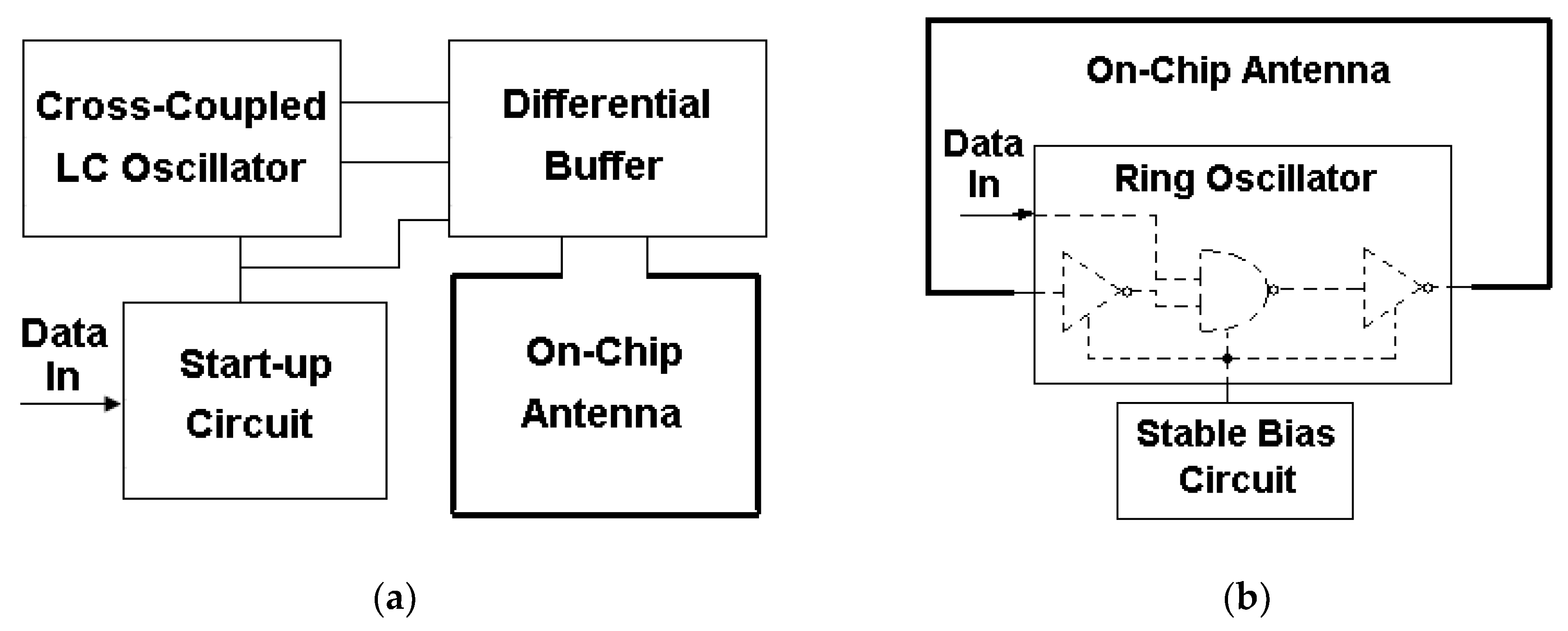
In each transmitter topology, the RF oscillator is the critical building block which mainly determines the overall performances of the transmitting architecture. LC oscillators offer high frequency stability over temperature, voltage, and process variations and low phase noise [
19]. These characteristics allow the use of these oscillator architectures in gigahertz applications. Among the different LC circuits typologies, Colpitts oscillators and cross-coupled topologies are the most frequently implemented in CMOS technologies. In Colpitts oscillators, the loop voltage gain must be very high to sustain oscillation, especially when low quality factor integrated inductors are employed in the resonator tanks, which implies a higher power consumption with respect to cross-coupled architecture [
20]. Finally, although ring oscillators (RO) have poor phase noise characteristics compared to LC oscillators, they have the advantages of a wider oscillation frequency range and a smaller layout footprint. The phase noise characteristics can be enhanced by implementing a differential architecture [
21] to the detriment of the power consumption and die size.
In this paper, two monolithic and totally different transmitter typologies, each exploiting an integrated small electrical loop antenna to radiate sufficient power for short range communication, are discussed. For the first time, a direct comparison between these two transmitters, realized with the same CMOS process, is presented. In particular, the experimental characterization, the radiating properties, and the feasibility of using the implemented systems in conjunction with a commercial receiver are reported. The transmitters, which are realized in a standard 3.3 V 0.35 µm CMOS process, implement an on–off keying (OOK) modulation and are designed to be duty cycled.
3. LC Oscillator-Based Transmitter
3.1. Oscillator Design
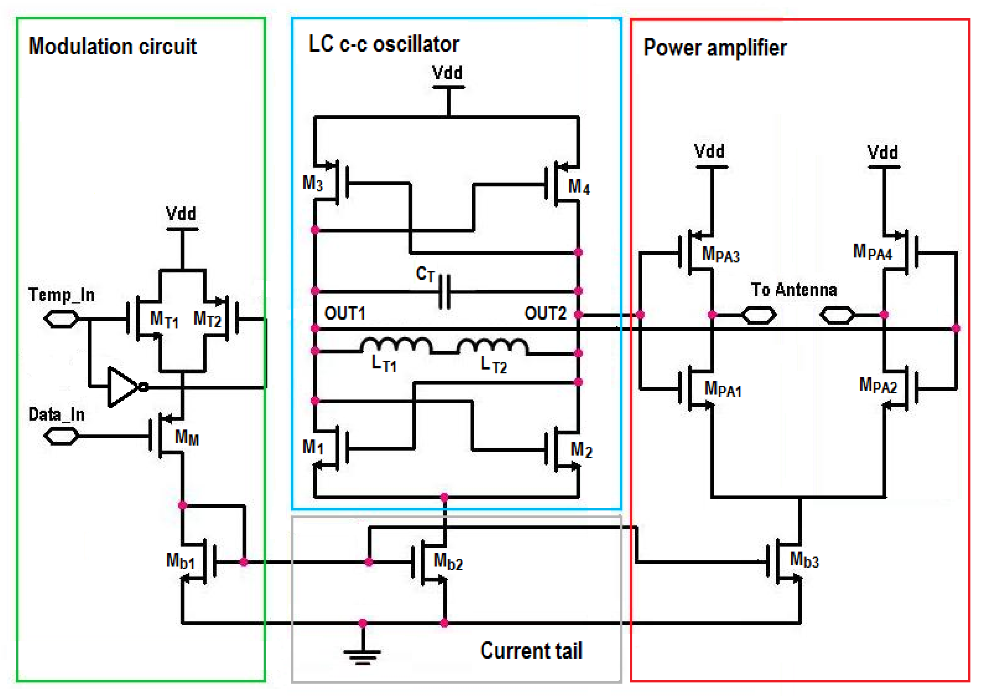
The implemented oscillator was based on a complementary cross-coupled LC topology [
22,
23], whose schematic is depicted in
Figure 2.
Despite the simplicity of the cross-coupled differential scheme, the complementary architecture featured a higher negative transconductance Gm useful for overcoming the resonating circuit losses, essentially due to the parasitic resistance of the tank, and sustaining oscillations. In a monolithic oscillator the complementary topology is thus preferable, because it allows oscillations to also start for low quality factor (QTank) resonating circuits, usually due in turn to the poor quality factor, QL, of the integrated inductors.
The proposed oscillator was implemented exclusively with standard transistors provided by the four metal layers AMS CMOS 0.35 µm technology.
Figure 2 depicts the transmitter schematic, where each section is highlighted.
The resonating circuit employed simple square, four-turns, spiral inductors fabricated in the top aluminum metal layer and a polysilicon capacitor, both provided by the 0.35 µm process. The employed coils exhibited a quality factor of 4.7 at 2.5 GHz. Two 2.6 nH components were exploited for maintaining a balanced differential circuit. Using two series inductors also made it possible to increase the tank resistance and thus the output voltage swing for a given bias condition. The polysilicon capacitor value was set for getting a 2.5 GHz oscillation frequency. Each transistor had a width/length ratio of 72 μm/0.35 μm to achieve the needed negative transconductance for sustaining oscillations. Furthermore, the sizes of the cross-coupled pairs, together with the current tail, were chosen to properly bias the differential power amplifier (PA) described in the next section.
3.2. Power Amplifier
Typical power amplifiers employ RF chokes to obtain the required power transfer to the antenna. Furthermore, matching networks, positioned between the PA and the antenna, are used to maximize the power delivered to the radiating element.
In the present transmitter, a simple source coupled differential amplifier was implemented to feed the small loop antenna. The circuit, depicted in
Figure 2, was DC coupled to the oscillator that provided the sufficient output voltage swing for switching the amplifier. The antenna was connected between the differential outputs of the PA. The circuit worked as follows. Let us assume that OUT2 in
Figure 2 is at the maximum voltage value, OUT1 is thus at the minimum one. In this case, the
MPA3 p-channel Metal-Oxide-Semiconductor (PMOS) of the first branch of the amplifier is on and feeds a certain current into the antenna. On the other branch of the circuit, the
MPA2 n-channel Metal-Oxide-Semiconductor (NMOS) device is on, allowing the current that flows through the loop structure to be steered to ground. Hence, the following theoretical maximum power
PAnt can be transmitted to the antenna:
where
Vdd is the supply voltage,
Vdsat_O the saturation voltage of the current tail, and
IO the bias current of the PA.
The differential pair was accurately sized through electrical simulations for maximizing the power delivered to the directly connected antenna, modeled as discussed later. In particular, two polysilicon capacitors were inserted between the PA output, i.e. at the loop input, and ground for obtaining the electrical resonance of the antenna. A width/length ratio of 65 μm/0.35 μm was set to draw a DC current of about 3 mA through the loop.
3.3. Modulation Circuit
The left box of
Figure 2 contains the circuit used to implement the OOK modulation. The
Data_In signal was the modulating signal, that, applied to the PMOS current source, made it possible to alternately power on and off the transmitter. To further reduce the power consumption, an
1:n current mirror was implemented. In particular, the ratio with respect to the current tail of the oscillator was fixed to 1:5. Moreover, the
Temp_In signal, which can be provided by a digital control circuit, was required for enabling the transmission gate by connecting the supply voltage to the current mirror (
MM,
Mb1,
Mb2,
Mb3) and, thus, for temporizing the transmitter.
4. Ring Oscillator Topology
Conventional current-starved single-ended ROs are usually employed for realizing wide tuning range, voltage-controlled oscillators by exploiting the dependence of the large signal oscillation frequency
fOsc on the bias current
Ib [
24,
25], which is determined by:
where
N is the number of inverters used,
tD the time delay of each stage,
VOsc the oscillation amplitude, and
C the load capacitance.
Furthermore, in a RO topology the small-signal amplitude of the oscillating signal can be expressed as:
where
vOut(0) is the initial condition at the RO output,
As the gain of each amplifier stage, and
ωs the −3 dB bandwidth of each stage [
20]. The first term of (3) represents the time-varying amplitude of the oscillations. Therefore, the settling time can be expressed to a first approximation as:
The settling time of an RO, at a given initial condition, depends only on the amplifier stages characteristics (gain and bandwidth). To obtain a fast start-up oscillator, required for low power transmitters, bias current and hence devices sizes have to be properly set. Moreover, the oscillator must provide a stable carrier for implementing an OOK modulation transmitter. For achieving this purpose, a bias current with high robustness against supply voltage fluctuations can be employed to feed the oscillator.
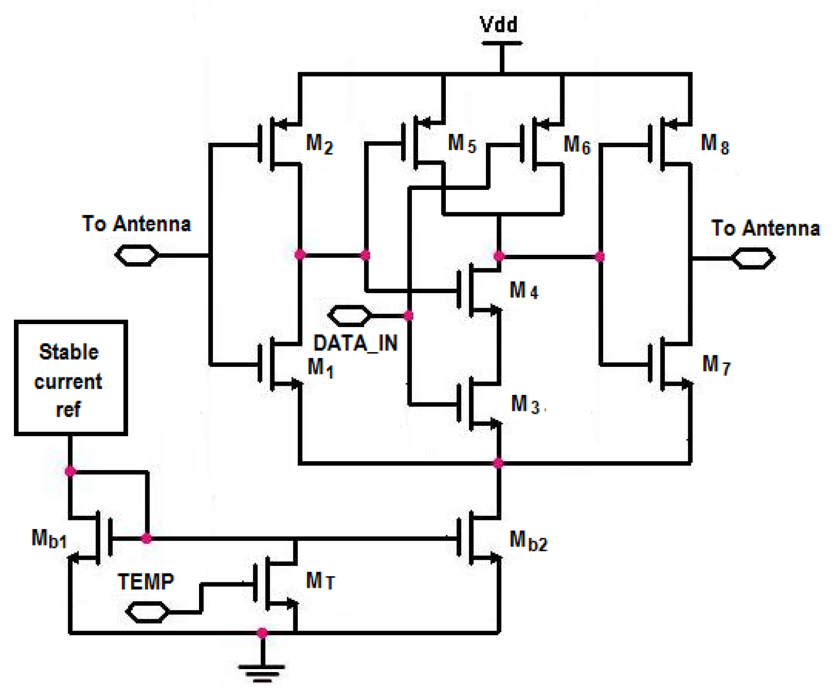
Figure 3 shows the schematic of the RO-based transmitter.
The oscillating circuit was implemented using three single-ended inverting stages that were biased by a current tail in a mirror configuration, where a high stable current reference was exploited. The OOK modulation was implemented by exploiting a NAND gate, one of the two inputs of which was the modulating signal. The transmitter could be also duty-cycled by means of the control signal TEMP that enables the transistor MT, which makes it possible to short-circuit the current tail input terminal to ground, thus powering off the oscillator. The inverting stages were sized together with the current tail to get about 1 GHz oscillation frequency. The device sizes of the CMOS inverters were 7 μm/0.35 μm (W/L ratio) and 19 μm/0.35 μm for NMOS and PMOS, respectively, while the transistor sizes of the NAND gate were 10 μm/0.35 μm (NMOS) and 14 μm/0.35 μm (PMOS). The bias current was about 1.5 mA.
5. Integrated Antennas Design
The use of an on-chip antenna is economical and well suited for short-range applications like RFID based systems. However, the chip size of CMOS tags limits the dimensions of the radiating element to be integrated, thus it is not possible to obtain resonance condition at 1 GHz and 2.5 GHz. At these frequencies, in fact, well-tuned antennas should be a few tens centimeters long. Hence, an electrically small loop antenna is actually the only choice. Moreover, because of its shape, a loop structure is a good solution for realizing an integrated antenna, since it can surround the whole chip and, consequently, maximize its area.
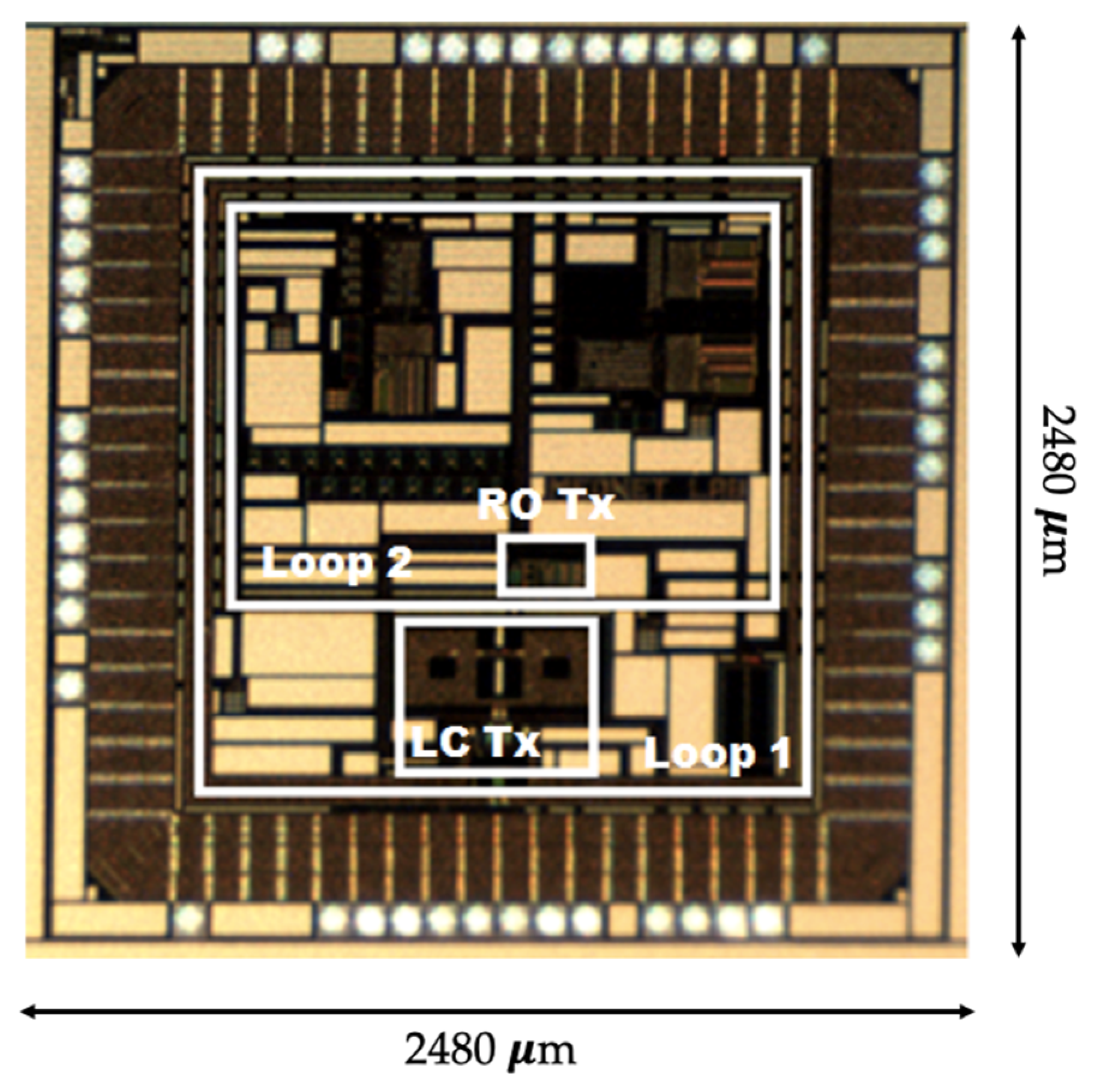
Two separate radiating elements were implemented to avoid the use of a switch that could further degrade the antenna performance. Two single turn rectangular loops were realized using the top aluminum metal layer of the standard 0.35 µm CMOS process, based on a silicon substrate with a resistivity ρ = 19 Ω⋅cm. The first antenna, which was connected at the PA outputs of the LC-based transmitter, covered an area of 1620 × 1620 µm
2, with a trace width of 20 µm and a feeding gap of 139 µm. The second one, which was fed by the RO, occupied an area of 1520 × 1088 µm
2, with a trace width of 20 µm and a feeding gap of 70 µm. A microphotograph of the chip outlining the integrated antennas is shown in
Figure 4.
The linear sizes of the loops are less than one tenth of the respective carrier wavelength, λ, they are fed at, thus they can be treated as electrically small antennas. In this condition, a small electric loop shows a magnetic linear dipole behavior and it can be analyzed, to a first approximation, using a circuital model composed of the series of an inductance
L and two resistances, a radiation resistance
Rrad and a loss resistance
Rloss, which describe the radiation performance and the loss of the structure, respectively. The inductance and resistances values can be calculated by the following formulas [
26]:
where
P is the perimeter of the square loop in meters, λ the wavelength in meters,
Pw the cross section length of the wire rod,
f the frequency in Hertz,
μ the magnetic permeability,
σ the metal conductivity in S/m,
l the loop side length in meters, and
b is the wire radius in meters.
Moreover, the effectiveness of an antenna can be evaluated using the radiation efficiency
erad. This parameter is given by the ratio of the radiated power to the total power dissipated by the antenna. Furthermore, the antenna gain
G is directly related to the radiation efficiency. These parameters can be calculated using the following expressions [
26]:
where
D is the directivity of the antenna and has a maximum value of 1.5 for a small loop antenna.
Table 1 contains the calculated theoretical parameters of the loop structures described before, which are, however, valid in vacuum and only for a first level analysis. Worse performances can be expected from the on-chip antennas due to the losses associated with the thick silicon substrate, the on-chip metallization used to form the antennas, and the interferences of the nearby circuits and metal wires, which reduce the radiation efficiency [
10,
27].
Each radiating element was directly connected to its own transmitter. The test chip did not have bond pads attached to the antennas to avoid load effects. The feeding devices of each transmitter topology were sized through electrical simulations to deliver the maximum power to the respective radiating element modeled, as described above.
6. Experimental Results
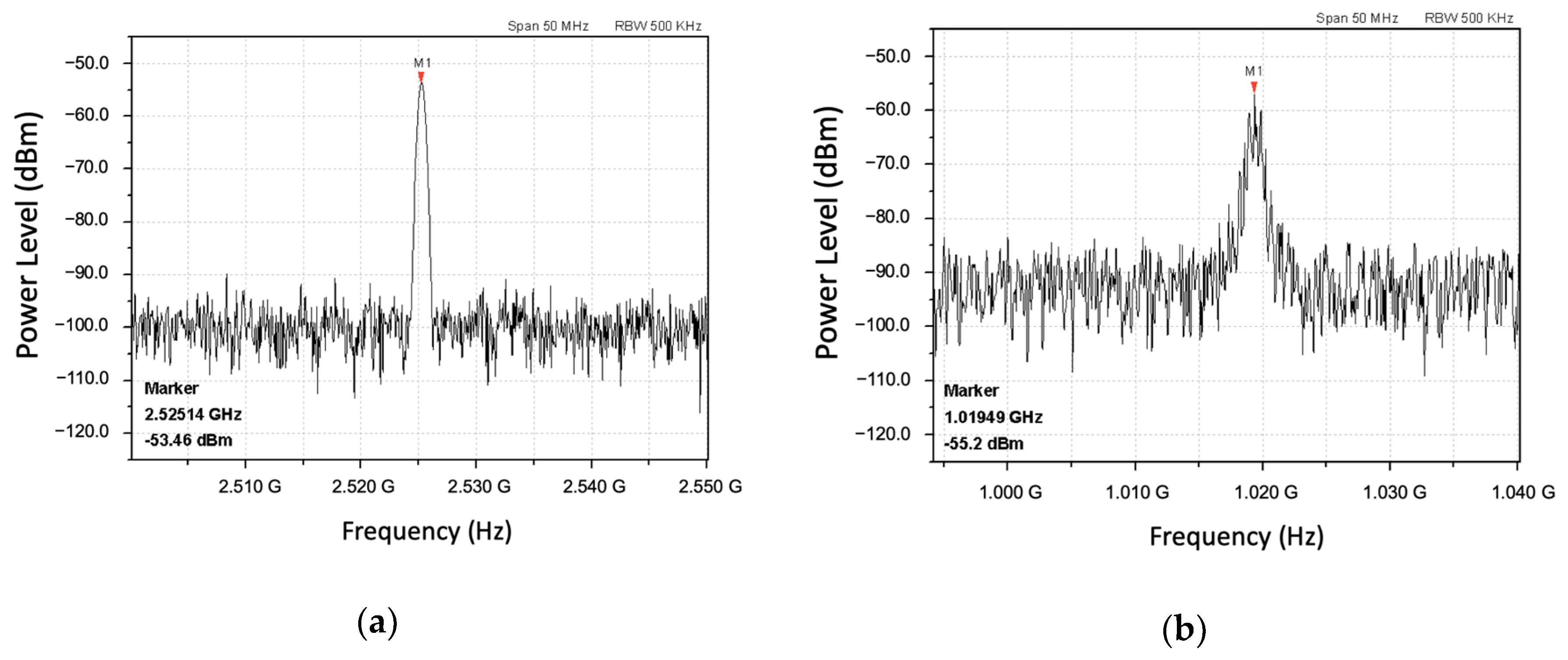
After fabrication, the test chips were packaged in 48-pin DIL packages. The RF performance of the implemented transmitters was characterized using a 0.4/3 GHz bandwidth, 5 dBi logarithm periodic dipole antenna (model R&S HL040) connected to an R&S FSV signal, and spectrum analyzer acting as the receiver.
6.1. Transmitters Performances
The experimental measurements show a carrier frequency of the complementary cross-coupled LC oscillator-based transmitter of about 2.53 GHz with a phase noise of −87 dBc/Hz at 1 MHz offset. The RO-based typology had a carrier frequency of about 1 GHz with a phase noise of −71 dBc/Hz at 1 MHz offset. The obtained results are limited by substrate properties, quality, and thickness of dielectrics (SiO
2) and conductors of the four metal layers of the AMS CMOS 0.35 µm technology. The phase noise was estimated as follows:
where
L(∆
f)
dBc is the phase noise,
Ps is the power level of the noise in a band of 1 Hz to a certain offset frequency from the carrier,
Pc is the power level of carrier frequency, and
RBW is the bandwidth resolution of the spectrum analyzer.
Figure 5 shows the received spectra from both transmitters.
The cross-coupled LC transmitter and the RO topology consumed, respectively, 22 mW and 4.8 mW from 3 V supply voltage. As the PA had a separate bias pad, we measured that the LC oscillator used 13 mW of the above mentioned total dissipated power. The maximum data rate of the on-off keying modulation supported by the transmitters is essentially limited by the start-up time of the oscillators.
The LC-based transmitter required about 480 ns to settle from power-up, hence allowing a maximum data rate of approximately 2 Mbit/s, whereas the RO-based topology performed a settling time of about 1 μs that limited the on-off keying modulation rate to almost 1 Mbit/s.
Transmitting 1 kbit packet once in a second at the maximum data rates resulted in an average power consumption of 11 µW when the LC transmitter was used, and 5 µW for the RO-based topology.
In
Table 2 the performances of the proposed transmitters are summarized and compared. The LC-based transmitter exceeded the RO-based transmitter performances, showing a better phase noise and a higher data rate, at the expense of a doubling of the power consumption.
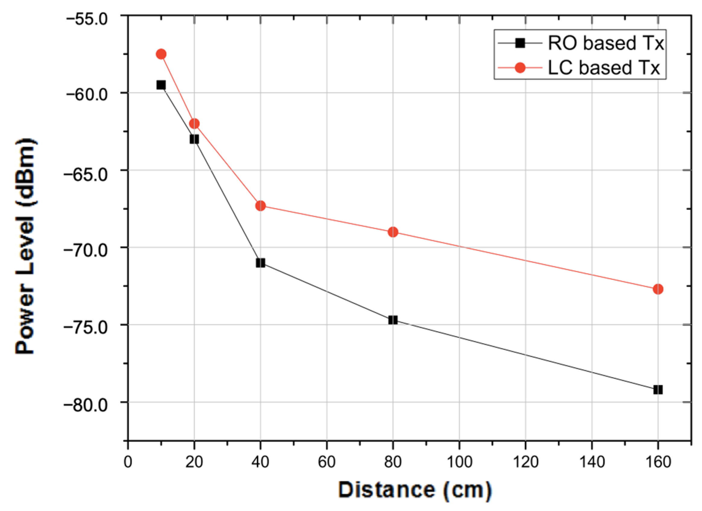
6.2. Radiation Properties
To evaluate the radiation performance of the implemented transmitters, the chip was mounted on a printed circuit board (PCB) for allowing pins access and power supply by a 3 V battery. The test board was shielded with aluminum foils, with the exception of a window in direction of the top of the IC, to minimize the antenna effect of the PCB and the possibility of off-chip spurious emission and for noise reducing purposes. Since each radiating element was fully integrated with its transmitter, the two RF sections can be characterized as monolithic circuits [
28].
Figure 6 reports the measured received power recorded at different distances from the receiver, namely the spectrum analyzer, in the antennas maximum gain. Measurements do not take into account the influence of the antenna near field. The power consumption of the circuit was 22 mW at 2.53 GHz for the LC-based Transmitter and 4.8 mW at 1 GHz for the RO-based Transmitter.
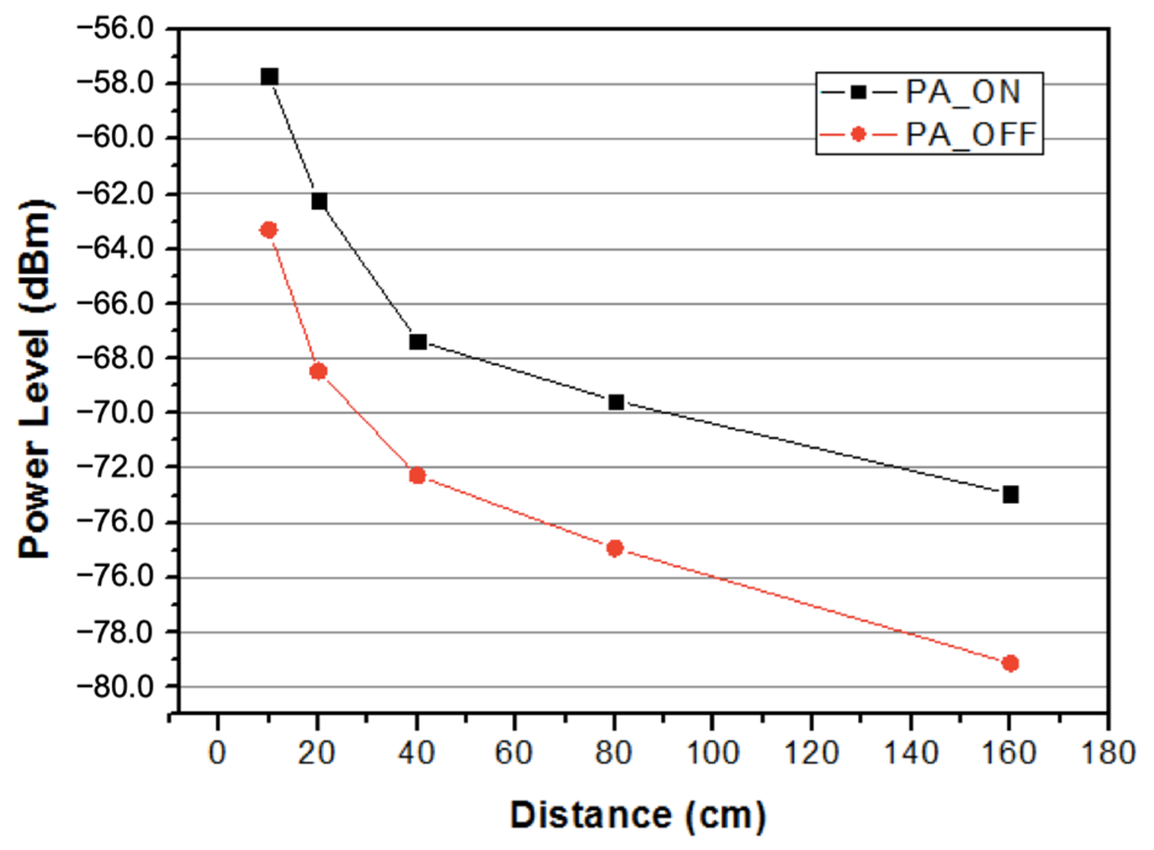
The radiating effect of the LC tank was evaluated by powering off the PA, and thus grounding the connected antenna.
Figure 7 shows the recorded power levels at different distances between transmitter and receiver when the PA was on and off.
The radiating effect of the inductors made it possible to establish an RF link with a transmitted power level approximately 7 dBm lower than the case in which the antenna was fed by the PA. Starting from this result, the front-end performance can be calculated, and in particular the power-added efficiency (PAE), defined as:
where
Prf,out is the RF output power,
Prf,in the RF power at the input of the PA,
Pdc the total power drawn by the PA from the DC supply. As the implemented monolithic front-end section (PA + antenna) added 5 mW of RF power (+7 dB) to the transmitted signal and drew 9 mW from 3 V supply voltage, the PAE was equal to about 55%.
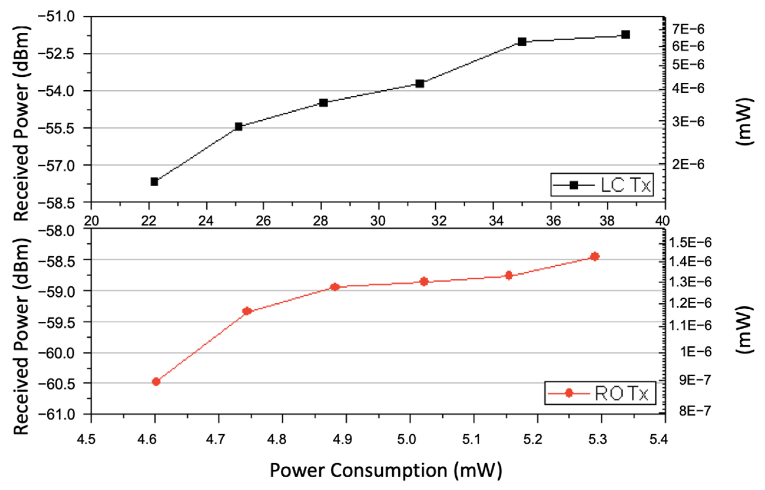
Finally, the radiated power of the two transmitter topologies was measured by sweeping the supply voltage from 2.7 V to 3.3 V, and therefore the power consumption of the circuits. The results are shown in
Figure 8, from which we conclude that the RO-based RF link exhibited a higher power efficiency.
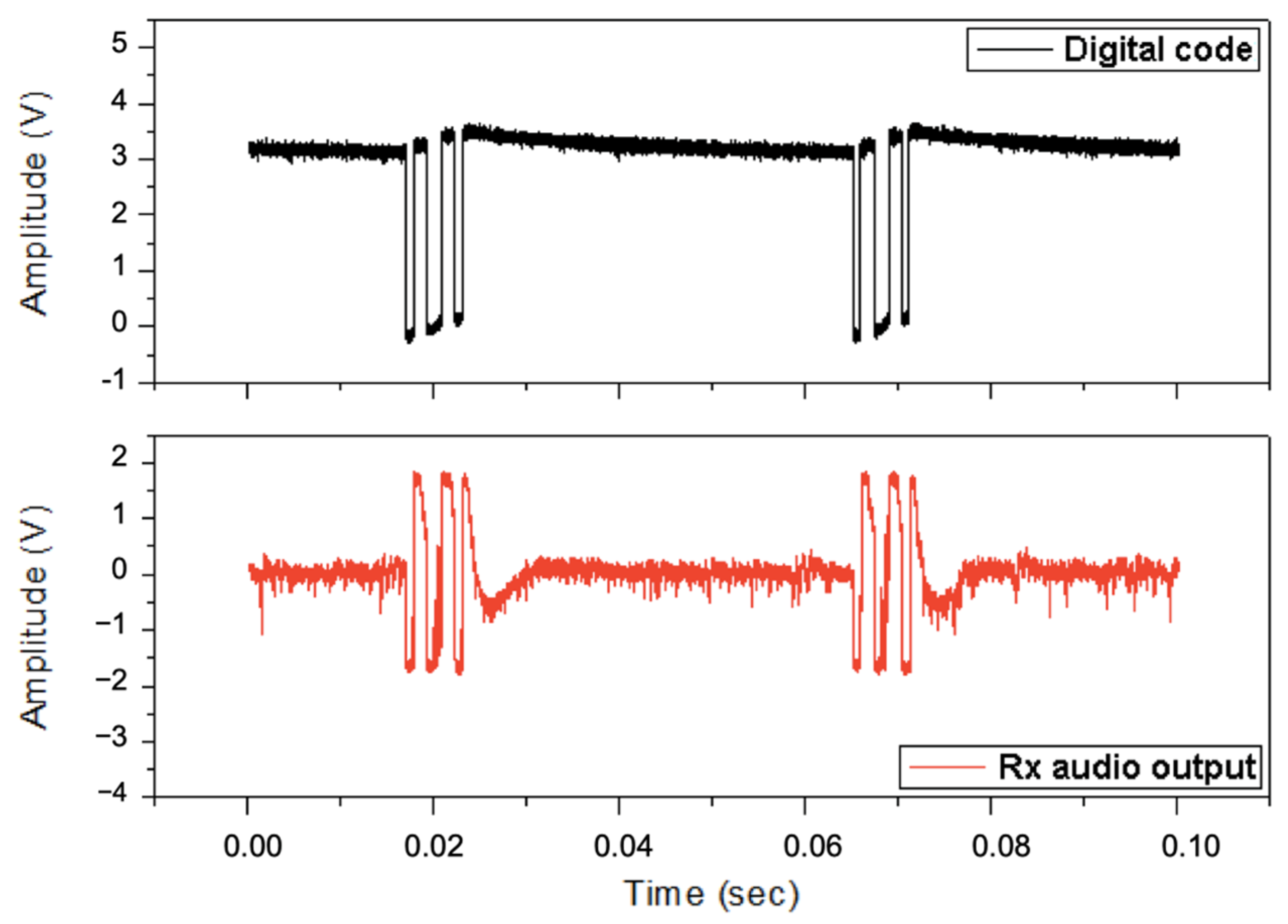
6.3. Code Transmission Feasibility Test
The capabilities of the discussed circuits to transmit an OOK modulated packet of data were tested using a digital code, stored in the device, as the modulating signal. The feasibility of using the implemented system in conjunction with a commercial receiver was proven by employing a hand-held ICOM IC-R20 unit, a 0.15–3300 MHz receiver allowing SSB, CW, AM, FM, and WFM demodulation modes. Setting the IC-R20 on the WFM mode, the demodulated signal was detected at the audio output of the receiver and plotted on an oscilloscope.
Figure 9 shows the recorded digital data. An RF communication channel of about 3 m was demonstrated, when transmitter and receiver were in line-of-sight.


