A Fast-Transient All-Digital LDO with Adaptive Clock Technique

Abstract
:1. Introduction
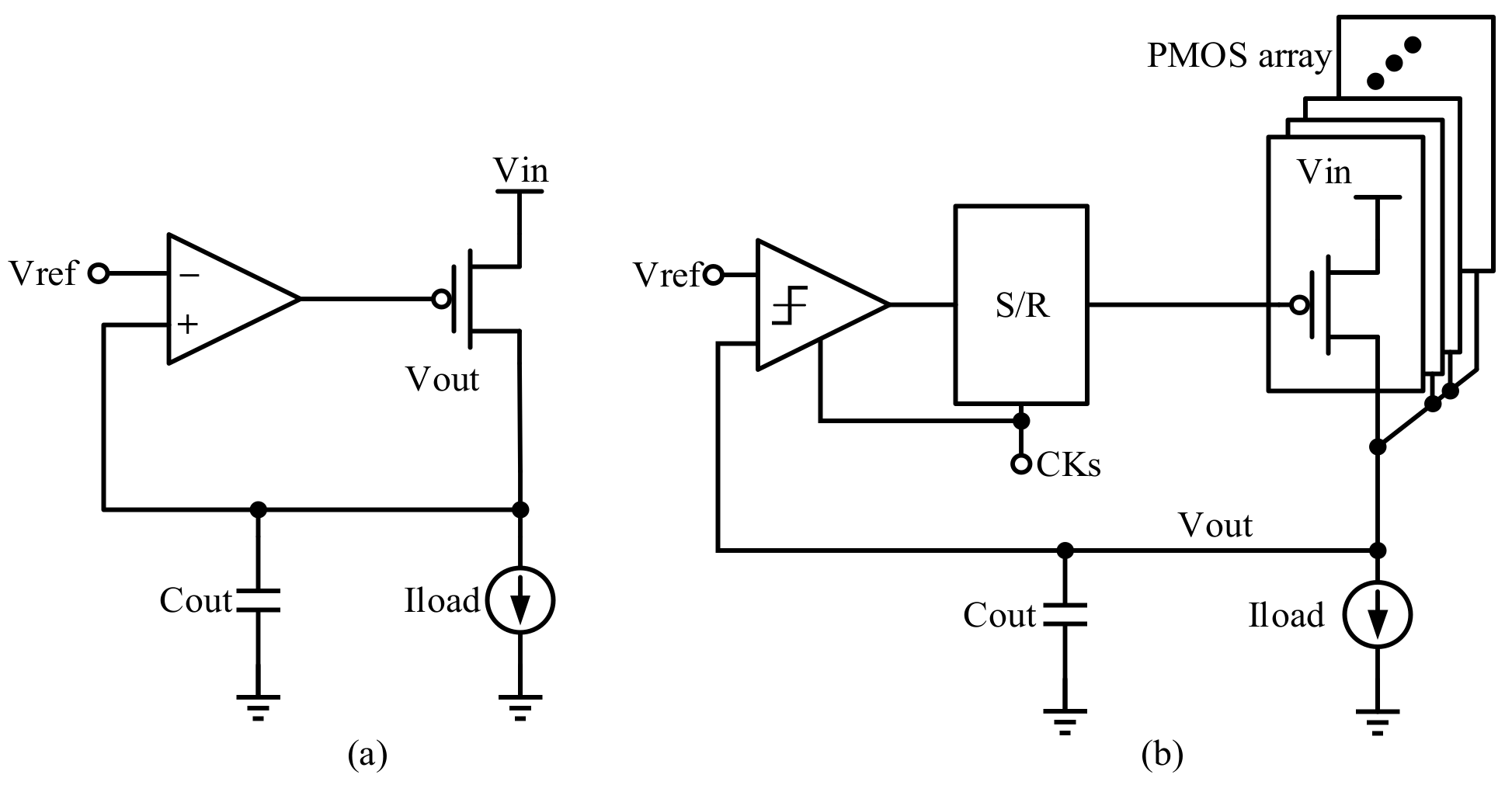
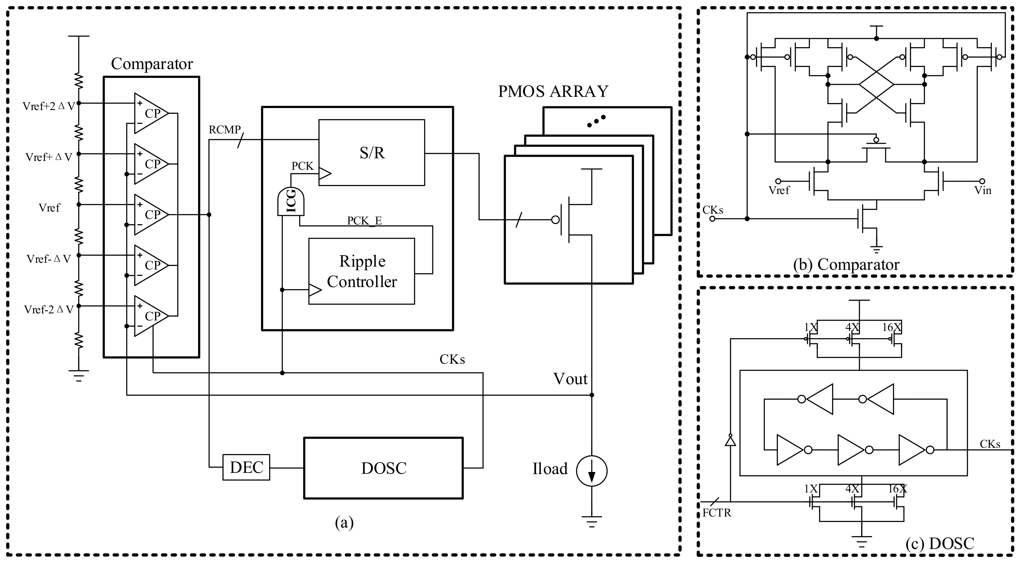
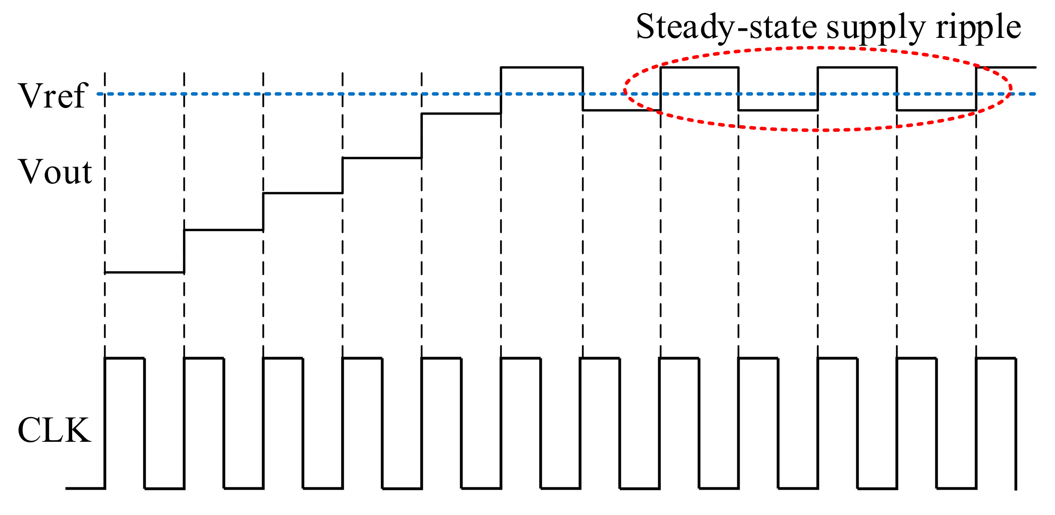
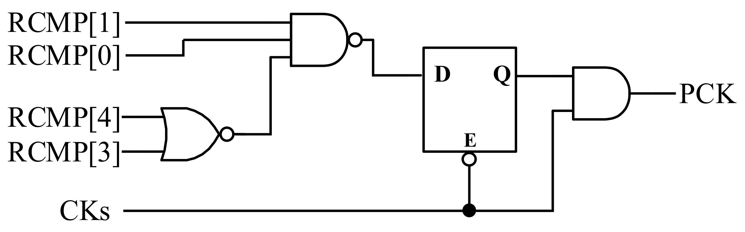
2. Proposed Technique
3. Design Consideration
The Value of ΔV
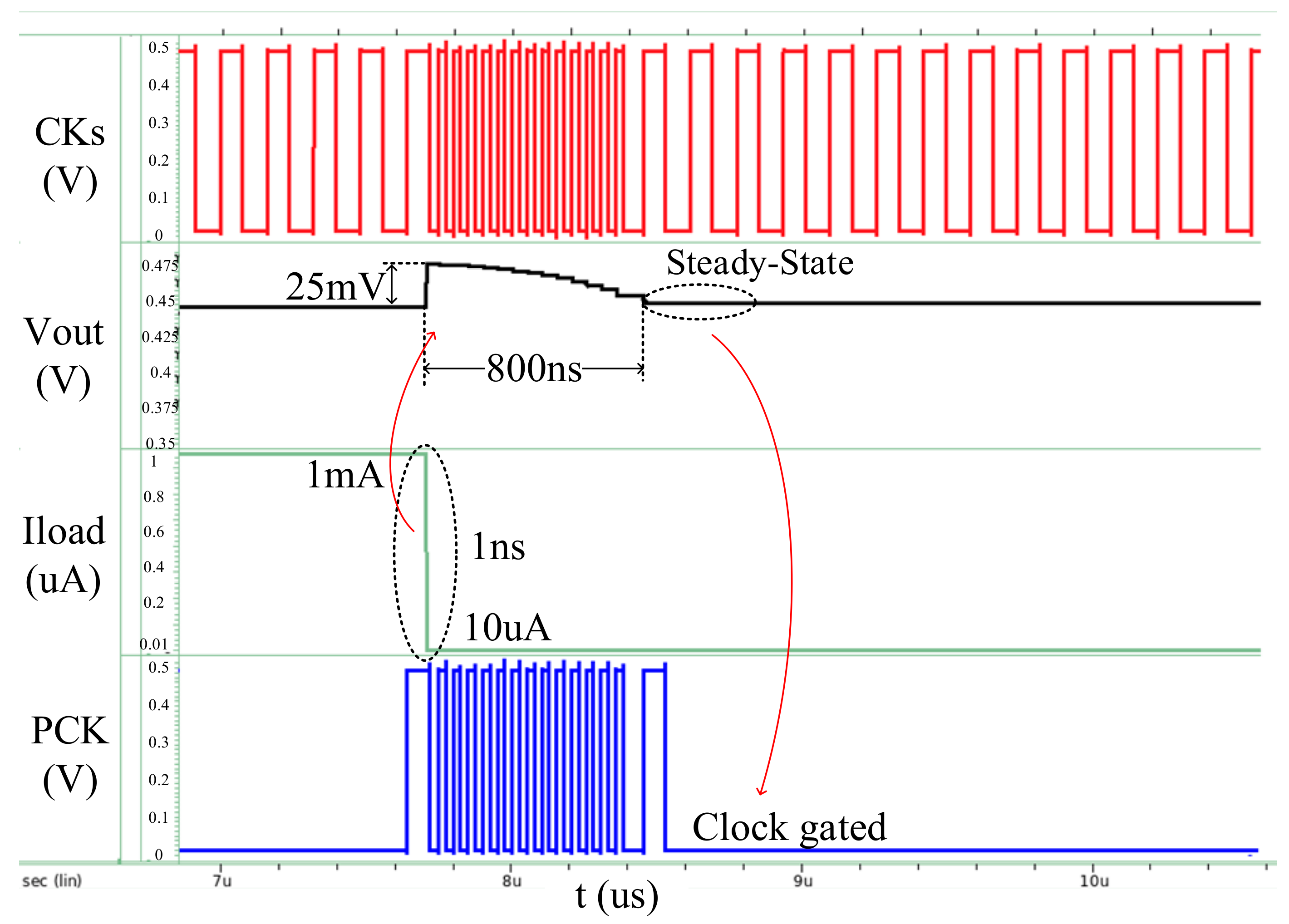
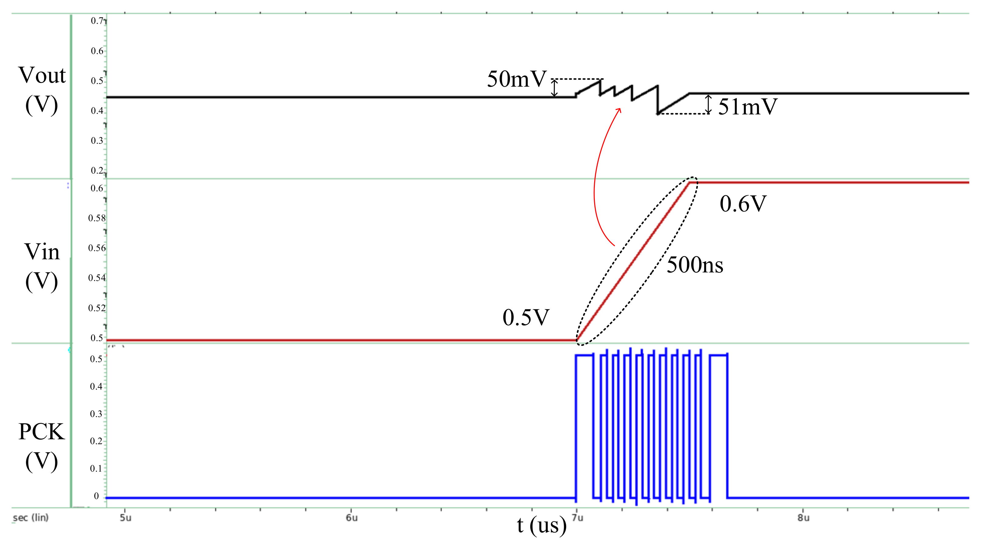
4. Experiments
5. Conclusions
Author Contributions
Funding
Acknowledgments
Conflicts of Interest
References
- Myers, J.; Savanth, A.; Prabhat, P.; Gaddh, R.; Toh, S.O.; Flynn, D. A 12.4 pJ/Cycle Sub-Threshold, 16 pJ/Cycle Near-Threshold ARM Cortex-M0+ MCU with Autonomous SRPG/DVFS and Temperature Tracking Clocks. In Proceedings of the 2017 Symposium on VLSI Circuits, Kyoto, Japan, 5–8 June 2017; IEEE: Piscataway, NJ, USA; pp. C332–C333. [Google Scholar]
- ur Rahman, F.; Kim, S.; John, N.; Kumar, R.; Li, X.; Pamula, R.; Bowman, K.A.; Sathe, V.S. A Unified Clock and Switched-Capacitor-Based Power Delivery Architecture for Variation Tolerance in Low-Voltage SoC Domains. IEEE J. Solid State Circuits 2019, 54, 1173–1184. [Google Scholar] [CrossRef]
- Bowman, K.A. Adaptive and Resilient Circuits: A Tutorial on Improving Processor Performance, Energy Efficiency, and Yield via Dynamic Variation. IEEE Solid State Circuits Mag. 2018, 10, 16–25. [Google Scholar] [CrossRef]
- Chang, K.-C.; Luo, S.-C.; Huang, C.-J.; Peng, J.-H.; Chu, Y.-H. MORAS: An Energy-Scalable System Using Adaptive Voltage Scaling. In Proceedings of the 2018 International Symposium on VLSI Design, Automation and Test (VLSI-DAT), Hsinchu, Taiwan, 16–19 April 2018; IEEE: Hsinchu, Taiwan; pp. 1–4. [Google Scholar]
- Yang, W.-B.; Lin, Y.-Y.; Lo, Y.-L. Design of Fast-Locked Digitally Controlled Low-Dropout Regulator for Ultra-low Voltage Input. Circuits Syst. Signal Process. 2017, 36, 5041–5061. [Google Scholar] [CrossRef]
- Shin, I.; Kim, J.-J.; Lin, Y.-S.; Shin, Y. One-Cycle Correction of Timing Errors in Pipelines with Standard Clocked Elements. IEEE Trans. Very Large Scale Integr. VLSI Syst. 2016, 24, 600–612. [Google Scholar] [CrossRef]
- Roy, A.; Calhoun, B.H. Exploring Circuit Robustness to Power Supply Variation in Low-Voltage Latch and Register-Based Digital Systems. In Proceedings of the 2016 IEEE International Symposium on Circuits and Systems (ISCAS), Montreal, QC, Canada, 22–25 May 2016; IEEE: Piscataway, NJ, USA; pp. 273–276. [Google Scholar]
- Lim, C.; Mandal, D.; Bakkaloglu, B.; Kiaei, S. A 50-mA 99.2% Peak Current Efficiency, 250-ns Settling Time Digital Low-Dropout Regulator with Transient Enhanced PI Controller. IEEE Trans. Very Large Scale Integr. VLSI Syst. 2017, 25, 2360–2370. [Google Scholar] [CrossRef]
- Nasir, S.; Gangopadhyay, S.; Raychowdhury, A. All-Digital Low-Dropout Regulator with Adaptive Control and Reduced Dynamic Stability for Digital Load Circuits. IEEE Trans. Power Electron. 2016, 31, 8293–8302. [Google Scholar] [CrossRef]
- Lee, Y.-H.; Peng, S.-Y.; Chiu, C.-C.; Wu, A.C.-H.; Chen, K.-H.; Lin, Y.-H.; Wang, S.-W.; Tsai, T.-Y.; Huang, C.-C.; Lee, C.-C. A Low Quiescent Current Asynchronous Digital-LDO with PLL-Modulated Fast-DVS Power Management in 40 nm SoC for MIPS Performance Improvement. IEEE J. Solid State Circuits 2013, 48, 1018–1030. [Google Scholar] [CrossRef]
- Okuma, Y.; Ishida, K.; Ryu, Y.; Zhang, X.; Chen, P.H.; Watanabe, K.; Takamiya, M.; Sakurai, T. 0.5-V Input Digital LDO with 98.7% Current Efficiency and 2.7-µA Quiescent Current in 65nm CMOS. In Proceedings of the IEEE Custom Integrated Circuits Conference, San Jose, CA, USA, 19–22 September 2010; IEEE: San Jose, CA, USA, 2010; pp. 1–4. [Google Scholar]
- Ramadass, Y.; Fayed, A.; Haroun, B.; Chandrakasan, A. A 0.16 mm2 Completely On-Chip Switched-Capacitor DC-DC Converter using Digital Capacitance Modulation for LDO Replacement in 45 nm CMOS. In Proceedings of the 2010 IEEE International Solid-State Circuits Conference-(ISSCC), San Francisco, CA, USA, 7–11 February 2010; IEEE: San Francisco, CA, USA, 2010; pp. 208–209. [Google Scholar]
- Zhao, L.; Lu, Y.; Martins, R.P. A Digital LDO With Co-SA Logics and TSPC Dynamic Latches for Fast Transient Response. IEEE Solid State Circuits Lett. 2018, 1, 154–157. [Google Scholar] [CrossRef]
- Gangopadhyay, S.; Somasekhar, D.; Tschanz, J.W.; Raychowdhury, A. A 32 nm Embedded, Fully-Digital, Phase-Locked Low Dropout Regulator for Fine Grained Power Management in Digital Circuits. IEEE J. Solid State Circuits 2014, 49, 2684–2693. [Google Scholar] [CrossRef]
- Huang, M.; Lu, Y.; Sin, S.-W.; Seng-Pan, U.; Martins, R.P. A Fully Integrated Digital LDO with Coarse–Fine-Tuning and Burst-Mode Operation. IEEE Trans. Circuits Syst. II Express Briefs 2016, 63, 683–687. [Google Scholar] [CrossRef]
- Kundu, S.; Liu, M.; Wong, R.; Wen, S.-J.; Kim, C.H. A Fully Integrated 40pF Output Capacitor Beat-Frequency-Quantizer-Based Digital LDO with Built-In Adaptive Sampling and Active Voltage Positioning. In Proceedings of the 2018 IEEE International Solid-State Circuits Conference-(ISSCC), San Francisco, CA, USA, 11–15 February 2010; IEEE: San Francisco, CA, USA, 2018; pp. 308–310. [Google Scholar]


| RCMP | Shift Step of S/R | Freq. of DOSC |
|---|---|---|
| 00000 | 3 | 12~350 MHz |
| 00001 | 2 | 9~200 MHz |
| 00011 | 1 | 6~100 MHz |
| 00111 | 1 | 6~100 MHz |
| 01111 | 2 | 9~200 MHz |
| 11111 | 3 | 12~350 MHz |
| RCMP | FCTR |
|---|---|
| 00000 | 000 |
| 00001 | 100 |
| 00011 | 110 |
| 00111 | 110 |
| 01111 | 100 |
| 11111 | 000 |
| others | 110 |
| Resistor Ladder | Comparators |
|---|---|
| 1 uA @0.5 V | 0.62 uA @0.5 V |
| This Work | [13] | [15] | [16] | |
|---|---|---|---|---|
| Process | 55 nm | 28 nm | 65 nm | 65 nm |
| Area (mm2) | 0.000503 | 0.019 | 0.01 | 0.0374 |
| Controller | quantized controller with a dead zone | quantized controller with a dead zone | quantized controller with a dead zone | quantized controller |
| Structure | Adaptive clock | S/R+TSPC | CFT | VCO based ADC |
| Loop bandwidth control mechanism | Fine-grained Fs scaling, Clock gating | Fs fixed | Coarse-grained Fs scaling | Coarse-grained Fs scaling |
| Synthesizable | Yes | No | Yes | No |
| Minimum VIN (V) | 0.5 | 0.6 | 0.6 | 0.6 |
| Nominal VOUT (V) | 0.45 | 0.55 | 0.4 | 0.4 |
| Max.ILOAD (mA) | 1 | 25 | 100 | 100 |
| COUT (nF) | 0.0001nF | 0.15 | 1 | 0.04nF |
| Min.IQ (uA) | 2.3 | 28 | 82 | 100 |
| Peak current efficiency | 99.99% | 99.96% | 99.92% | 99.5% |
| FOM * (ps) | 0.17 | 0.59 | 0.4 | 0.19 |
© 2019 by the authors. Licensee MDPI, Basel, Switzerland. This article is an open access article distributed under the terms and conditions of the Creative Commons Attribution (CC BY) license (http://creativecommons.org/licenses/by/4.0/).
Share and Cite
Yu, Y.; Yuan, J.; Qiao, S.; Hei, Y. A Fast-Transient All-Digital LDO with Adaptive Clock Technique. Electronics 2019, 8, 1422. https://doi.org/10.3390/electronics8121422
Yu Y, Yuan J, Qiao S, Hei Y. A Fast-Transient All-Digital LDO with Adaptive Clock Technique. Electronics. 2019; 8(12):1422. https://doi.org/10.3390/electronics8121422
Chicago/Turabian StyleYu, Yi, Jia Yuan, Shushan Qiao, and Yong Hei. 2019. "A Fast-Transient All-Digital LDO with Adaptive Clock Technique" Electronics 8, no. 12: 1422. https://doi.org/10.3390/electronics8121422
APA StyleYu, Y., Yuan, J., Qiao, S., & Hei, Y. (2019). A Fast-Transient All-Digital LDO with Adaptive Clock Technique. Electronics, 8(12), 1422. https://doi.org/10.3390/electronics8121422