Article

Low Cost Autonomous Lock-In Amplifier for Resistance/Capacitance Sensor Measurements

1
Group of Electronic Design I3A, Zaragoza University, Pedro Cerbuna 12, Zaragoza 50009, Spain
2
Department of Electronics, National Institute for Astrophysics, Optics and Electronics, Luis Enrique Erro 1, Puebla 72840, Mexico
3
Independent Research Professor, UVM Puebla, Camino Real San Andrés Cholula 4002, Puebla 72810, Mexico
*
Author to whom correspondence should be addressed.
Electronics 2019, 8(12), 1413; https://doi.org/10.3390/electronics8121413
Submission received: 24 October 2019 / Revised: 20 November 2019 / Accepted: 22 November 2019 / Published: 26 November 2019
(This article belongs to the Special Issue Low-Voltage Integrated Circuits Design and Application)

Abstract

:
This paper presents the design and experimental characterization of a portable high-precision single-phase lock-in instrument with phase adjustment. The core consists of an analog lock-in amplifier IC prototype, integrated in 0.18 µm CMOS technology with 1.8 V supply, which features programmable gain and operating frequency, resulting in a versatile on-chip solution with power consumption below 834 µW. It incorporates automatic phase alignment of the input and reference signals, performed through both a fixed −90° and a 4-bit digitally programmable phase shifter, specifically designed using commercially available components to operate at 1 kHz frequency. The system is driven by an Arduino YUN board, thus overall conforming a low-cost autonomous signal recovery instrument to determine, in real time, the electrical equivalent of resistive and capacitive sensors with a sensitivity of 16.3 µV/Ω @ εrS < 3% and 37 kV/F @ εrS < 5%, respectively.

Graphical Abstract

1. Introduction

Device miniaturization has been key to the development of innovative sensing technology with application in different fields [1], ranging from biology and medicine [2,3], to environmental monitoring [4,5,6], or limnology and civil structural monitoring [7,8,9]. Therefore, the interest in new large scale integrated systems including sensing technology is growing substantially, since they make it possible to carry out the same analysis usually performed by traditional sophisticated equipment but with the advantage of reduced size, power, and cost.
However, according to each application, different challenges are faced in the achievement of high performance low-voltage low-power (LVLP) miniaturized solutions, not only in terms of the sensing element but also in the necessary electronic instrumentation: the measurement system must adequately perform the sensor signal acquisition to recover the target information preserving accuracy and reliability, with real-time operation, portability, and through an intuitive and friendly interface to make it accessible to different users [2].
One of the main concerns in the acquisition system is the low amplitude sensor signal, often buried in high noise levels interfering with the whole detection, so a suitable recovery technique such as lock-in amplification is required [10]. A lock-in amplifier (LIA) is based on phase-sensitive detection (PSD), where the signal of interest (VIN, f0) is multiplied by a reference signal (VR) whose frequency is also set at f0 to perform a synchronous detection; the resulting signal is low-pass filtered with a suitable corner frequency to recover a DC component proportional to the amplitude of interest [10,11], according to:
VOUT_DC = 2AVIN cos θ/π + Vdd/2,
where A is the voltage gain of the LIA, θ is the VIN-VR phase shift, and a square reference signal VR is assumed. The term Vdd/2 is the common-mode voltage reference level for single Vdd supply systems compatible with battery operation. As the system presents the maximum sensitivity for the in-phase condition (θ = 0°), single phase lock-in amplifiers work with input and reference signals operating at the same frequency and in phase.
Commercial LIA equipment is non-portable, bulky and expensive, limiting the test scenario to specialized laboratories [12,13,14]. On the other hand, general purpose commercial integrated solutions of LIAs are almost nil since their building blocks involve specific and rigorous design requirements that cannot always be fully accomplished, presenting inconveniences as no amplification stage, limited resolution and offset susceptibility [15]. To solve these setbacks, a few analog LIAs integrated in CMOS technology can be found in the literature, mainly designed for the characterization of different kinds of sensors like magnetic, mechanical, optical or resistive [16,17,18,19,20]. However, when conditioning resistive/capacitive sensors with an AC excitation source, issues like phase shift, overheating or decoupling at high frequencies may arise. Both decoupling and overheating can be solved by choosing an appropriate operating frequency, but the phase shifting problem remains [21,22], so a phase adjustment circuit is required. In addition, phase adjustment allows for versatile/generic implementations that can be adapted to different sensors by recalibration and reconfiguration of the operating parameters [23].
The above mentioned integrated solutions consider only the read-out channel, but do not include the signal phase alignment (also called signal synchronization) circuit, which is crucial for the proper operation of the LIA. As a consequence, they require manual adjustment, thus losing autonomy and not being suitable for portable and remote applications. Therefore, it becomes necessary to develop a complete LIA-based recovery system profiting from the advantages of analog integrated prototypes in terms of LVLP and reduced size, while also including automatic phase alignment with a low-cost hardware efficient approach, so as to obtain a truly portable high-precision autonomous instrument [2].
This paper addresses the implementation of such an instrumentation board, based on an analog integrated lock-in amplifier [19] that exhibits low power consumption, flexibility due to its programmable gain and operating frequency and small size and compared to state-of-art LIAs, being therefore a very competitive choice in terms of large scale reproducibility [4,5,24], with an automatic signal synchronization system driven by an Arduino YUN board which manages all the measurement process and that acts as an intuitive interface between the processing system and the data storage in the PC [25]. The result is a complete portable and autonomous single-phase LIA measurement system able to detect low amplitude signals resulting from resistive or capacitive sensors, while at the same time performs an automatic phase shift adjustment independent of the input signal amplitude or its variations with a simpler and more flexible design compared to state-of-art solutions. Additionally, although not presented in this paper, the system can also be used as a dual-phase LIA for complex impedance measurements [26,27,28], which makes it very versatile and suitable for novel portable applications such as bio-impedance measurements.
The paper is organized as follows. Section 2 describes the proposed system, explaining the operation of its building blocks. Section 3 presents the experimental characterization of the whole system, as well as its validation through the impedance measurement of resistive and capacitive sensors. Finally, conclusions are drawn in Section 4.

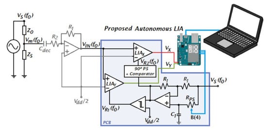
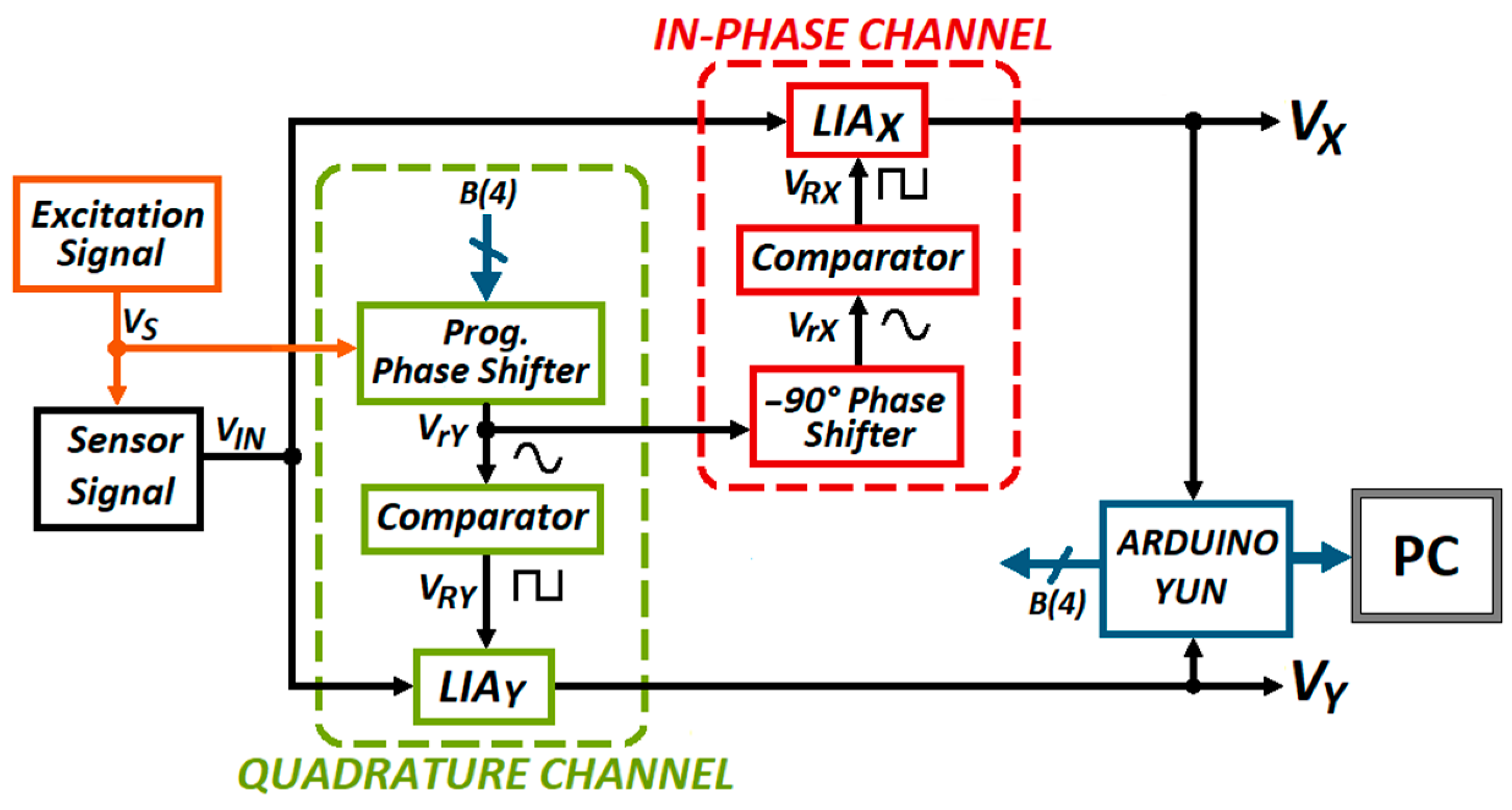
2. Proposed Lock-In Architecture

The block diagram of the proposed LIA-based measurement instrument is shown in Figure 1. It consists of two main stages: the in-phase channel (IP-Channel, X) and the quadrature channel (Q-Channel, Y), with identical PSD read-out (LIAX, LIAY) biased at a single Vdd and driven by quadrature reference signals VRX, VRY. Each channel includes a Phase Shifter (PS) that adequately adjusts the phase of the corresponding reference signals (VrX and VrY, sinusoidal), which are next converted by analog Comparators into 0-Vdd square signals (VRX and VRY) to perform the synchronous rectification. The DC output voltages (VX and VY) are acquired by the Arduino YUN platform, also in charge of the automatic signal phase alignment task, and finally data are stored in the PC.
The system operation when the information is contained in the signal amplitude is next explained in more detail. A source generator signal VS = AS sin(ω0 t) excites the sensor, typically placed in a voltage divider or a Wheatstone bridge configuration, whose output voltage signal [19,29] constitutes the LIA input VIN(t) = VIN sin(ω0 t + θ) for both channels. As reference signals VRX, VRY are in quadrature, from Equation (1) the output DC voltage of each channel can be written for a general situation as:
VX = 2AVIN cos θ/π + Vdd/2,
VY = 2AVIN sin θ/π + Vdd/2.
Thus, when the DC output signal for the Q-Channel is Vdd/2, VRX and VIN are either in phase or in counter-phase, and the change in VX is maximum for a given input voltage. Both solutions are actually valid operation conditions though, for simplicity, the X-Channel is called the in-phase Channel, as already mentioned.
To perform phase alignment, the output DC voltage VY in the Q-Channel is detected by the Arduino, which adjusts the Programmable Phase Shifter (PPS) by means of a 4-bit digital word B(4) = {b3, b2, b1, b0} until the condition VY = Vdd/2 is met. Then, the reference signal VrY in the IP-Channel is shifted −90° with a fixed PS to produce VrX, and the consequent digital reference signal VRX drives the PSD through the X-Channel. The maximum contribution of the DC level VX proportional to the amplitude of the input signal is thus obtained.
Note that this arrangement with an in-phase and an in-quadrature channel is equivalent to a dual phase LIA, which can recover both the magnitude and phase information, or equivalently the real (VX) and the imaginary part (VY), of electrical impedances [26]. Thus, the proposed system can be operated as single-phase LIA with automatic phase alignment, or as a dual phase LIA [26,27,28,30,31,32].

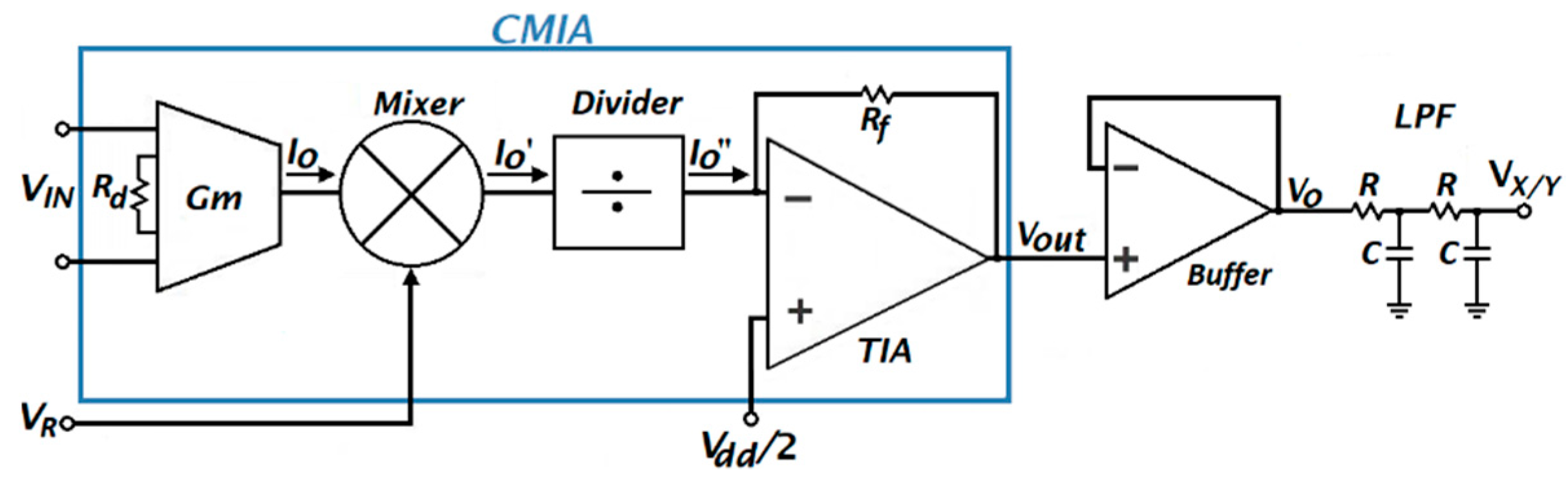
2.1. Lock-In Amplifier

As shown in Figure 2, the LIA consists of an integrated Current-Mode Instrumentation Amplifier (CMIA) in CMOS 180 nm technology with power supply Vdd = 1.8 V. A transconductance amplifier is used to convert the input signal into current, so the phase-sensitive detection is performed in the current domain, resulting in high linearity and reduction in area and power consumption compared with voltage mode implementations [19,33]. A Current Divider provides gain programmability to the amplifier, to adjust it as required for the application. Finally, the resulting signal is converted back into voltage through a transimpedance amplifier (TIA). This integrated CMIA is followed by a voltage buffer implemented with a low cost discrete Operational Amplifier (OA) HA17458 [34] for proper impedance coupling with the output Low Pass Filter (LPF).
The transistor-level schematics of the CMIA building blocks are presented in Figure 3, and briefly described below:
  • Transconductor: The input stage consists of a source degenerated differential pair with a negative feedback gm-boosting circuit as shown in Figure 3a. M1 transistors work as source followers, buffering the input signal to the degeneration resistor Rd. Thus, the VIN signal is converted into current (IAC = VIN/Rd) in a linear way and copied out by loading the A nodes with the output mirror branches with cascode transistors to improve the current copy, resulting in the IO signal.
  • Mixer: The phase-sensitive detection is performed in the current domain using a class AB current follower; the direction of the current IO is controlled by the square reference signal VR connected to the cascode transistors which act as switches. The fully rectified output current is I’O = (−1)VR ∙ IO, with VR = (0,1).
  • Current Divider: To provide gain programmability to the CMIA, a 3-bit current divider based on an R-2R ladder implemented with PMOS transistors in the triode region was used, achieving a highly linear current-division [35], according to:
    = 1 2 n [ 1 + j = 0 n 1 ( 2 j d j 2 j ) ]   with   n = 3 .
  • Transimpedance Amplifier: A single stage differential amplifier with a feedback resistor Rf = 100 kΩ converts back the signal into voltage domain. A compensation capacitor CC = 500 fF is used to ensure stability. The transfer function for the complete CMIA is:
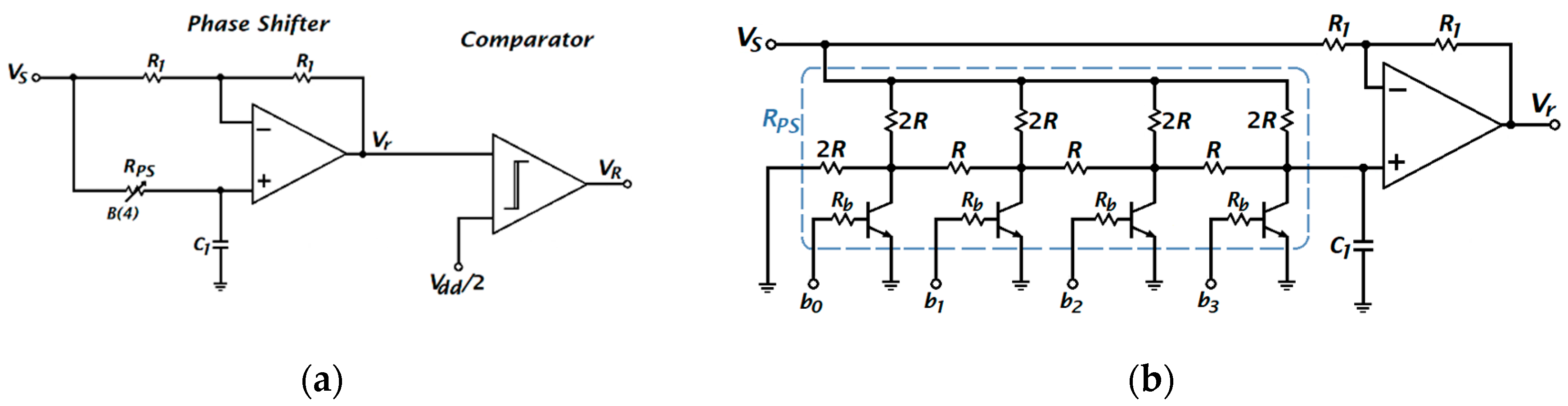
    V O U T V I N = ( 1 ) V R R f R d ( 1 2 n [ 1 + j = 0 n 1 ( 2 j d j 2 j ) ] )   with   n = 3 .
It can be seen that the gain depends mainly on the ratio Rf and Rd. Thus, both resistors were implemented with a high-resistivity polysilicon layer and will, therefore, suffer the same variations with process and temperature, thus ensuring good accuracy and robustness.
Finally, as shown in Figure 2, to complete the lock-in system, an external LPF was used. It consists of a second order passive RC network with R = 40 kΩ and C = 300 nF or C = 3 µF to set a cutoff frequency of 5 Hz or 0.5 Hz, respectively.
Note that the LIA can process either a single input signal by connecting the minus input terminal to Vdd/2, or a differential input signal. The prototype was experimentally characterized and used for the detection of small concentrations of carbon monoxide, providing a Dynamic Reserve, of 35.5 dB, which indicates that it is capable of recovering a signal submerged in noise levels 60 times higher [19,33]. In fact, the LIA can be seen as a Band-Pass Filter with a very high quality factor Q = f0/fLP, where f0 is the operating frequency and fLP is the LPF cutoff frequency, so it filters most of the noise contributions at frequencies different from that of the signal of interest. It has been chosen over other proposals of the authors [36,37] due to its good features in terms of input dynamic range, resolution, linearity, input referred noise, programmable gain, low power consumption and low integration area, which makes it a versatile and adaptable solution for different applications. Its main characteristics are summarized in Table 1.

2.2. Phase Shifter

Phase Shifters provide at their output a replica of the input signal with a phase displacement [38,39]. In our proposal, to perform phase alignment, two phase shifters, one variable (Q-Channel) and one fixed (IP-Channel), are required. Both are based on a simple topology that adjusts the signal phase by means of a passive element. The PS core topology is the first order OA-based All-Pass Filter (APF) [40,41] shown in Figure 4a. The phase angle:
θPS = 180° − 2 tan−1(2π ∙ RPSCf0),
depends on the passive elements RPS and C, as well as on the operation frequency f0. A frequency f0 = 1 kHz was chosen to avoid any contribution of low frequency flicker noise, and because it matches the typical operation frequency of biosensors used to characterize electrodes, organs and tissues, an application field where this portable low-cost approach can provide significant advantages over classical laboratory equipment [19,28,42,43,44].
The sine wave Vr is converted into a square reference signal VR (Figure 4a) by means of a comparator, which introduces a delay which depends on f0, causing an additional phase shift of 16° for f0 = 1 kHz. As a result, the resulting phase angle of the entire adjustment block is:
θVR = θPS − 16°,
For the IP-Channel, a PS with constant −90° phase shift is required. Therefore, considering Equation (6), R1 = 1 kΩ, C1 = 100 nF and RPS = 1.25 kΩ are used. The Q-Channel uses the same values of R1, C1, and the variable resistor RPS presented in Figure 4b, which consists of a programmable R-2R ladder (R = 10 kΩ). Through the activation or deactivation of its branches, by means of the 2N2222A BJT transistors [45] acting as switches controlled by a 4-bit digital word B(4) = {b3, b2, b1, b0}, the equivalent resistance can be adjusted in an easy and fast way. A larger number of bits leads to a wider tuning phase range with finer tuning steps, but also leads to an increase in the number of components in the R-2R ladder. A 4-bit resolution was chosen to get an adequate phase adjustment with a small amount of components driven by a very simple program.
Simulations were carried out with NI Multisim. A signal VS = 100 mV at 1 kHz was used and the RPS resistance was set to vary from 10 kΩ to 0.63 kΩ, obtaining a phase displacement θPS ranging from approximately 18° to 137° (Figure 5a), so that the overall θVR varies from 2° to 120° for the 4-bit PPS. The conversion of Vr to a square reference signal VR was also verified by simulation. Figure 5b shows the signals before and after the comparator, where the desired waveform, voltage range (0–1.8 V) and phase adjustment are achieved. Experimentally, both PS and comparators were implemented with discrete dual OA HA17458 [34].
Note that it is necessary to design the passive elements (RPS or C) based on the target frequency. This is why, for a general purpose instrument, the PS implementation is externally done through commercially available components, but for a specific application operating at a given frequency, a fully integrated solution can be considered.

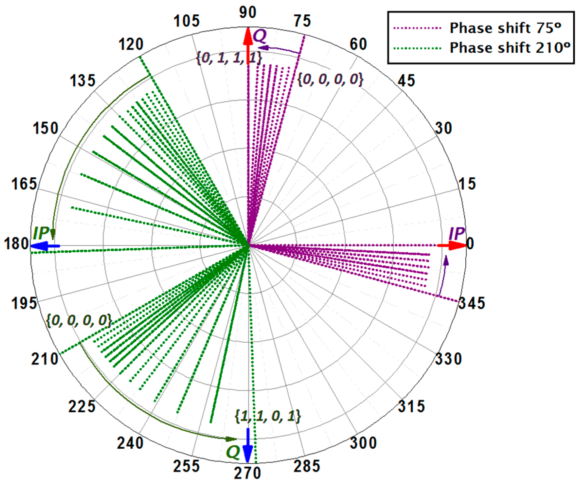
2.3. Phase Alignment and Data Transmission Interface

The automation of the phase alignment and measurement processes has the advantage of increasing both speed and reliability, as well as reducing operation costs compared to manual execution [5]. That is why, for the operation of the system, the Arduino YUN [46] platform was used. It has a microcontroller with digital and analog input/output ports, it is compatible with the technology used, and it is also easy to manage and program, while widely available [47].
As for the programming, constants and variables for measurement and control are first defined, and inputs/outputs (I/O) are assigned. Next, the phase shift control word is initialized to B(4) = {1, 1, 1, 0} to set θVR = +90°, and the output of both channels is recorded. If phase alignment is needed, i.e., if VY ≠ Vdd/2, a cycle begins in which B(4) is initialized to {0, 0, 0, 0} and increased to adjust the phase shift provided by the PPS, until the quadrature condition is reached at the output of Q-Channel. Then, the system finishes the phase tuning step and the measurement process begins: with the last saved value of B(4), the data of IP and Q Channels (VX and VY) are recorded. The flow chart of the program is detailed in Figure 6.

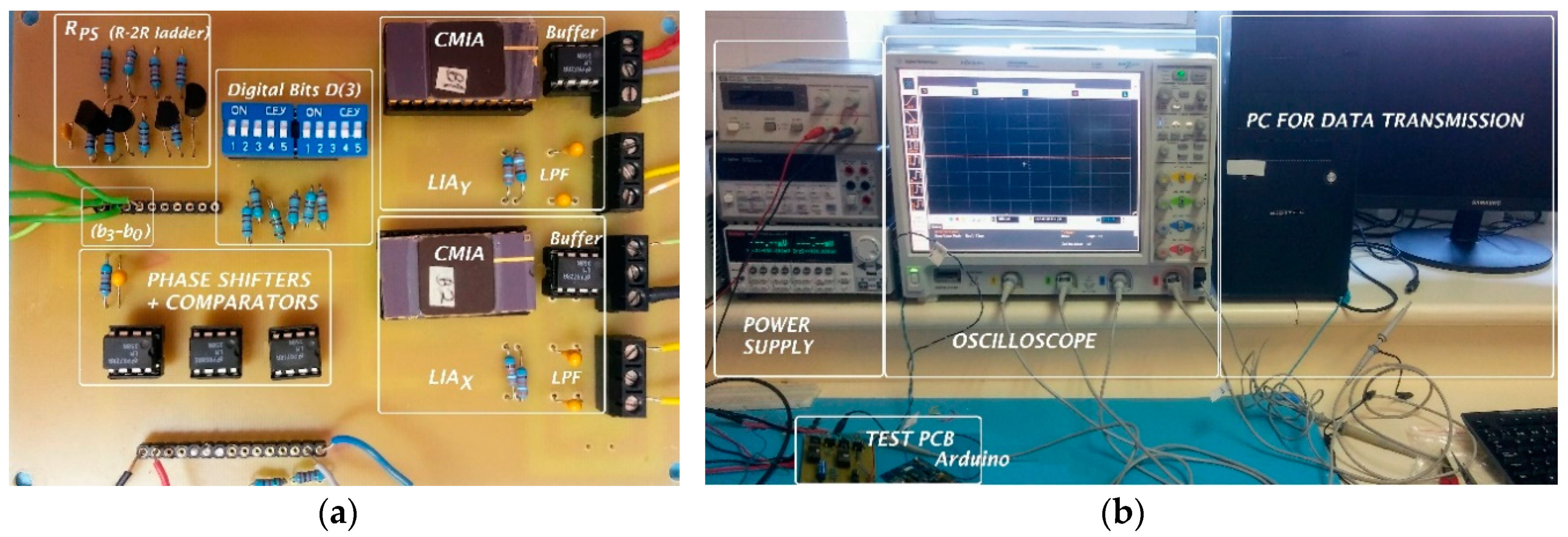
3. Experimental Results

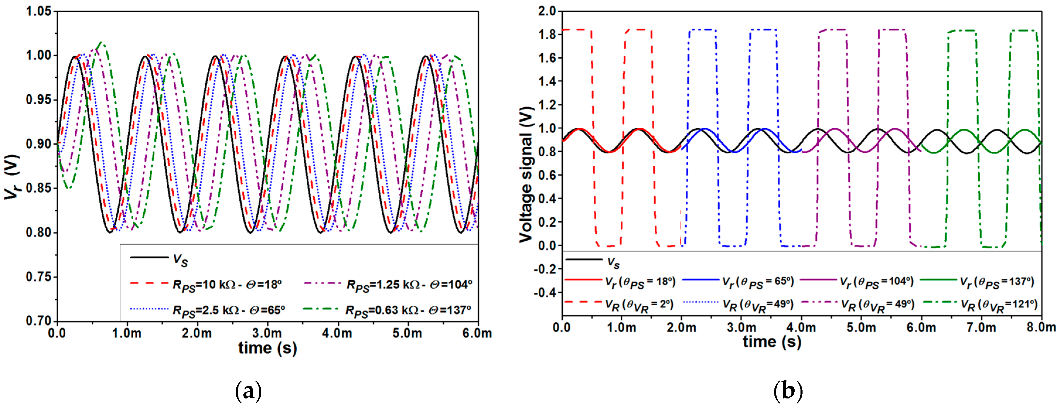
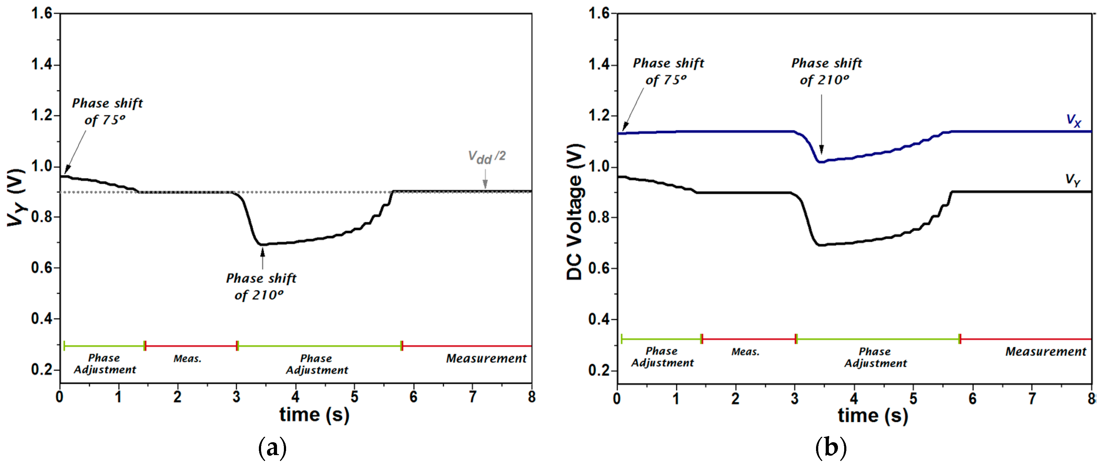
3.1. Autonomous Lock-In Performance

The whole system board is shown in Figure 7a. It incorporates two integrated CMIAs in CMOS technology, discrete components and the Arduino YUN. The system has a silicon area of 0.026 mm2 and PCB area of 10 × 14 cm2, constituting a solution easily transportable and cheap to implement. The integrated system uses Vdd = 1.8 V, discrete components (OA) use 3.3 V power supply, while BJT transistors are turned on/off with 5 V from the Arduino platform. Figure 7b shows the laboratory equipment used to perform the experimental characterization: a Keysight E3611A power supply, Keithley 2602 Source Meter Unit (SMU), Tektronix 4104 Oscilloscope and a computer using Universal Serial Bus (USB) for data transfer with Arduino.
Note that the Arduino microcontroller limits the resolution to 4.9 mV (10 bits from ground to 5V). As the resolution of the integrated CMIAs is 25 µV [33], a microcontroller of the Microchip group such as the PIC24FJ128GC010 with 16-bit ADC or equivalent could be used to increase the resolution of the LIA to 55 µV.
The proper operation of the PPS circuit was first tested. VS and VrY signals were monitored to check the signal phase displacement for each resistor value, as shown in Figure 8. Based on the measured phase shift, the real resistive value in the R-2R network was estimated according to Equation (5), to compare theoretical and measured data. Table 2 shows that the phase displacement becomes wider as RPS is decreased. Thus, first fine and then coarse phase tuning is performed, which results in fast adjustment to the desired value. Good matching between the calculated and the measured data is observed, with a phase absolute error εap ≤ 1.5° which in turn corresponds to a maximum relative error in the output voltage ε due to phase misalignment of 0.03%, an overall phase adjustment range of 236° and a phase resolution of 2°. The 4-bit resolution is therefore enough in practical cases to get high accuracy.
As already mentioned, there are two valid solutions to operate the single-phase LIA: with VIN and VRX in phase or in counter-phase, i.e., with a final phase shift between VIN and VRY of 90° or 270°. Figure 9 shows the phase adjustment steps in the Q-channel in both cases, starting with a 0 or 180° phase shift between VIN and VRY. Note that from 120° to 180° (300° to 360°), a 60° range of adjustment is lost. It is worth mentioning that this issue can be solved by increasing the number of bits or redesigning the R-2R ladder to obtain a smaller value of RPS. Even though it was not experimentally implemented, it was verified by simulation that the ideal RPS range of values for f0 = 1 kHz would be from 10 kΩ to 50 Ω to cover the entire phase adjustment range.
As explained in Section 2.3, during the phase adjustment the control word B(4) is initialized to {1, 1, 1, 0}, so θ = 90°. If VYVdd/2, B(4) is set to {0, 0, 0, 0} and starts increasing while monitoring VY until it crosses Vdd/2, and the last digital word B(4) after the crossing occurs is saved. For a more friendly-user operation, the Arduino was programmed to provide VX > Vdd/2 even in the counter-phase condition.
For the complete system characterization, sinusoidal signals VIN and VS were generated separately in order to modify the VIN phase externally. The signals were chosen within the dynamic range of each block, namely VIN = 6 mV and VS = 600 mV, both at 1 kHz. An initial random phase shift of 75° between VR and VIN was set. The system performs the calibration process until VY output satisfies the quadrature condition, and then the measurement process is started. This procedure was repeated for an initial phase shift of 210°, chosen again in a random way just to verify that the calibration and measurement processes were performed correctly.
The steps in phase that the PPS circuit performs for both phase shifts in the Q-Channel, and how the IP-Channel follows the same steps but with a constant −90° shift, are shown in Figure 10, where it is verified that both channels are adjusted to operate in the required phase conditions.
It is important to notice that the offset was calibrated: the systematic output offset of each LIA were measured at no signal level, then those values were subtracted from the experimental dc output values VX and VY through the Arduino program before storing the measured data to the PC.
The VY output is displayed in Figure 11a. Considering the cut-off frequency of the LPF, during the calibration stage a delay of 120 ms was added at each digital bit change (b3-b0) to allow VX and VY to be properly established. When the quadrature condition is satisfied, i.e., VY = Vdd/2, the in-phase condition is set for the IP-Channel and the measurement procedure can begin. For this test, the phase adjustment and measurement processes were performed in periods of approximately 2 seconds each. During these same measurements, the VX voltage was also monitored as shown in Figure 11b, where the two outputs, VX and VY, for the cases of 75° and 210° phase shifts are presented. When VY = Vdd/2, the VX output shows the expected DC voltage (1.139 V with relative error εrV = 0.2%), meaning that VIN and VRX signals are in-phase.
Table 3 summarizes the experimental system performance corresponding to different initial phase shifts. The ideal values of VX and VY were calculated by using Equations (2) and (3), respectively. Even though, as shown in Figure 11, adjustment was achieved much faster for 75° than for 210° initial phase-shift, calibration is correctly performed in a few seconds with relative errors εrV below 0.7% for the VY output. Besides, VX output meets the in-phase condition with a relative error εrV below 0.2%. It is worth mentioning that the relative error presented by the system is also affected by the gain mismatch between LIAs. However, the system manages to overcome this problem by presenting an error εrV below 1% in both output channels.

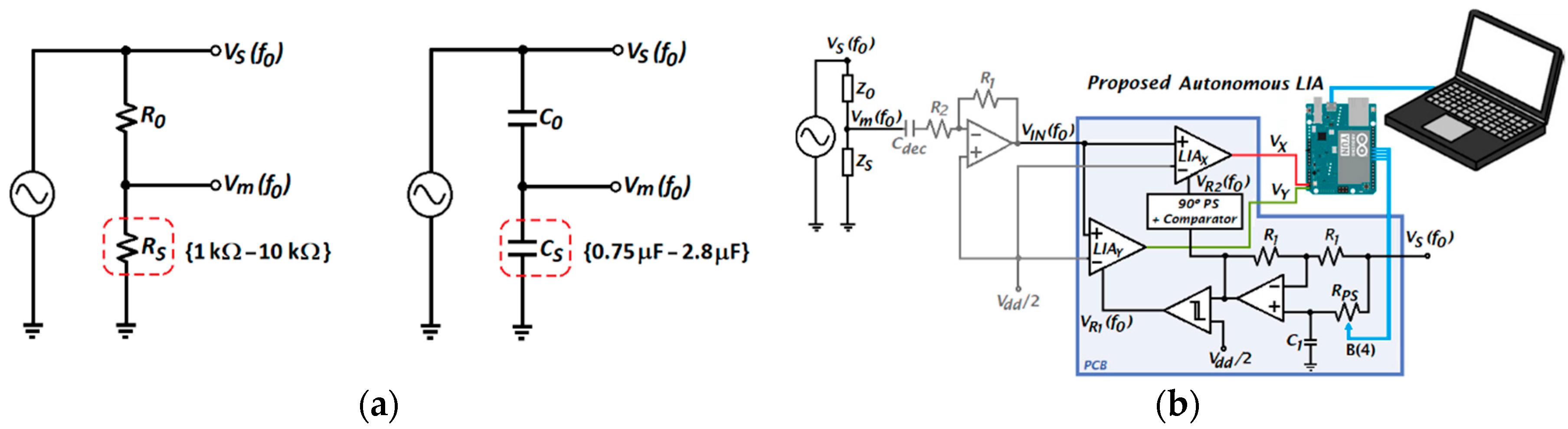
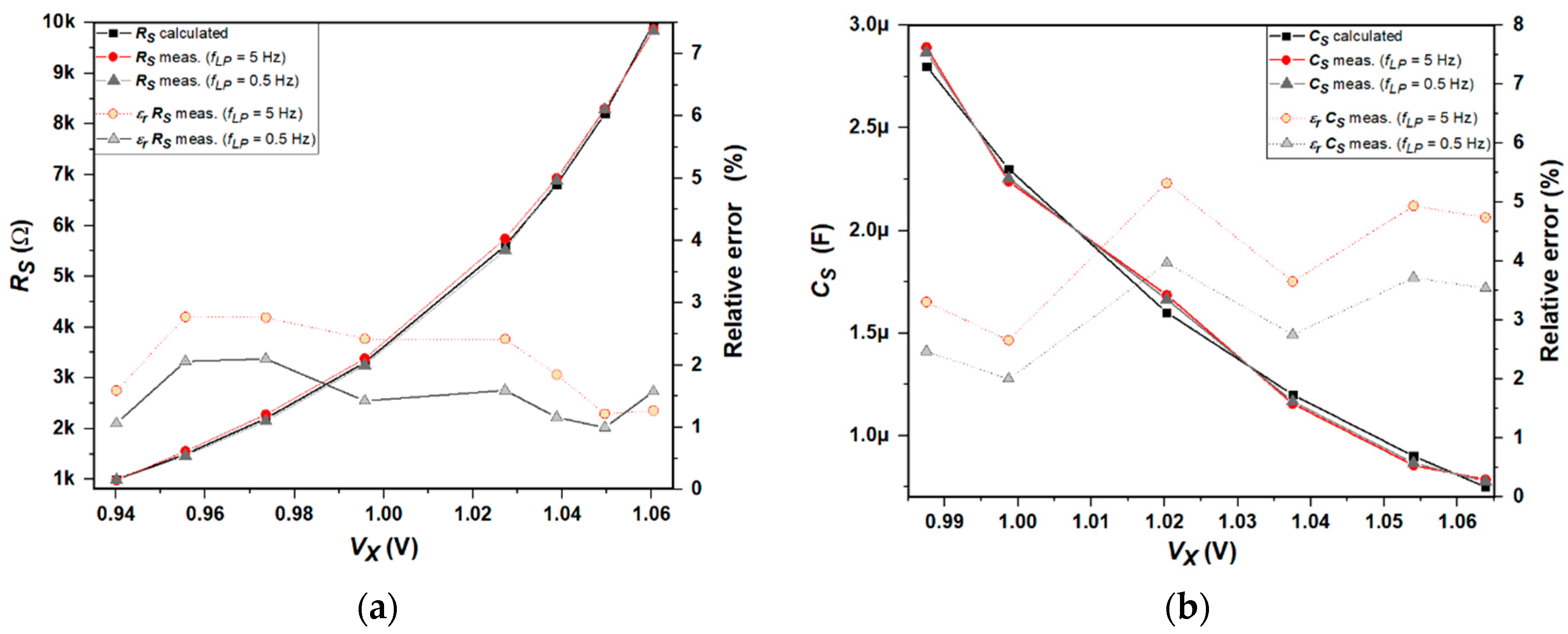
3.2. Impedance Measurements

Once the reference signals VRX and VRY are in phase and in quadrature with the input signal, respectively, the final 4-bit PPS digital word is saved and the measurement process begins. Measurement of non-complex impedances, either purely resistive or capacitive, is possible with single-phase LIA operation, i.e., by monitoring the in-phase channel VX output. However, if the sensor consists of a complex impedance, with both resistive and capacitive components, the system should be used as a dual-phase LIA where both outputs deliver the complete information of the sensor [26,27]. In this work, the proposed LIA system is characterized as a single-phase instrument with phase alignment for low-amplitude resistive and capacitive sensors measurements, since in previous works [33,36] the circuit noise immunity was already tested. The electrical equivalent of resistive and capacitive sensors was measured under controlled environmental conditions to eliminate any variation due to temperature, humidity, and light.
The measurement setup system is shown in Figure 12. Figure 12a shows the electrical symbol of the resistive and capacitive sensors with a tolerance of 2% and 5%, respectively, that were placed into a voltage divider and stimulated with a sinusoidal signal VS = 600 mV at 1 kHz, with reference resistor R0 = 5 kΩ and reference capacitor C0 = 1.6 µF, respectively. The sensors were previously measured independently to determine their real value, therefore, the estimated value of the resistive and capacitive sensors based on the measured voltages is compared with the exact value of the sensor. This way, the accuracy of the proposed LIA when determining the sensors values can be quantified.
The values of the reference impedances in each case where chosen to maximize the detection of variations at Vx output and improve the data collection of the Arduino YUN platform. Figure 12b presents the connection diagram of the whole system. Coupling between the sensing circuit and the LIA was made by means of a decoupling capacitor Cdec = 1 µF followed by an analog inverter which was used to further reduce the Vm signal amplitude, in this case, 100 times (R2 = 100 × R1) at the input of the LIA, in order to emulate a more realistic bio-signal test (in the order of 0.01–10 mV [48,49]).
The gain of both LIAs was set at maximum (42 dB) and the inverter and LIAs common mode input were connected to the required Vdd/2 DC level. Finally, the Arduino platform was the interface between the measurement system and the PC, as previously explained, allowing to control the phase alignment and store the measured data.
In Figure 13 the VX and VY outputs for resistive and capacitive sensors are displayed and compared to the theoretical values. It can be observed that information on the resistive (Figure 13a) and capacitive (Figure 13b) sensor is provided by VX, while VY output remains equal to Vdd/2 in both cases.
Based on the experimental LIA output voltages, the resistive and capacitive sensor values are determined by:
RS = R0/[(ACMIA R1 VSR2 VX) − 1],
CS = C0·[(ACMIA R1 VSR2 VX) − 1].
Figure 14 shows the RS and CS sensor values obtained from these equations. It can be observed in both cases that the use of a smaller cut-off frequency for the LPF results in higher measurement accuracy. For the first case (Figure 14a) the system presents a sensor measurement relative error εrS lower than 3%; for the second case (Figure 14b) the relative error εrS is below 5% in the determination of the capacitive value. The proposed system operating at maximum gain has a measurement sensitivity of 16.3 µV/Ω and 37 kV/Farad for resistive and capacitive sensor, respectively.
Finally, Table 4 presents a comparative of the proposed Lock-in Amplifier with other recent LIA solution. Even though special emphasis was made on searching solutions focused on a single phase LIA with phase alignment, only a few papers were found [50,51], implemented with discrete components or, as the proposed system, consisting of a mixed approach. However, it should be noted that in [50] and [51], three and four PSDs are required, respectively, for a single measurement output, while in the proposed LIA only two PSD are used, and it can be configured as a single or dual phase LIA.
Besides, in [50] the DC output voltages are measured by a data acquisition board (DAQ), which is a bulky module that reduces autonomy. On the other hand, the proposed solution not only uses a portable platform (Arduino) but also offers a wider frequency range from 0 to 125 kHz and input dynamic range (4.5–17 mV) with a resolution of 25 µV, faster phase calibration (<2.5 s) and smaller silicon power consumption. Thus, it constitutes a more versatile, hardware efficient and power efficient solution for phase adjustment without degrading the performance on integrated LIAs prototypes.
Alternatively, in [18,20,26,27,31] the implementation of a dual phase LIA is chosen to avoid the dependence with the phase of the input signal, being oriented to bioimpedance measurement. These papers are also included in the comparison. The proposed LIA shows greater versatility and flexibility compared to those solutions, as the phase alignment circuit can be enabled/disabled for its use as single-phase or dual-phase LIA. In addition, the gain adjustment (25–42 dB) as a function of the input signal amplitude, the reduced power consumption (834 µW for integrated prototypes and 7 mW for the whole system) and smaller silicon area (0.026 mm2), high sensitivity, and compatibility with microcontrollers as Arduino YUN, that enable fast data acquisition, make it a suitable and adaptable option for its use in truly portable applications.

4. Conclusions

A fully autonomous single-phase lock-in amplifier solution has been proposed in this article, implemented with two integrated CMIAs in CMOS UMC 180 nm technology and Arduino YUN platform. The discrete implementation was designed to have adjustable high gain and phase in order to measure signal amplitude or electrical impedances without degrading the performance of the CMOS integrated prototypes. It has a resolution of 25 µV, with sensor sensitivity of 16.3 µV/Ω @ εrS < 3% and 37 kV/F @ εrS < 5% for resistive sensor and capacitive sensor measurements, respectively. The low power consumption of 834 µW and low integration silicon area of 0.026 mm2 of the two CMIA prototypes, in addition to its capacity to be used as a dual-phase LIA, make it highly suitable for portable devices and innovative applications such as bio-impedance measurements. Besides, its compatibility with microcontrollers, in this case Arduino YUN, allows it to be adapted to different applications within the operating ranges of the CMIA.

Author Contributions

All authors contributed substantially to this paper. The conceptualization and methodology, P.M., M.T.S.-P. and J.O.; software, J.O.; validation, P.M.; formal analysis, investigation and resources P.M., B.C. and M.T.S.-P.; data curation, P.M. and J.O.; writing—original draft preparation, P.M.; writing—review and editing, P.M., M.T.S.-P. and B.C.; funding acquisition, P.M., M.T.S.-P. and B.C.

Funding

This research was supported by CONACYT CB-2015-257985 Research Project, TEC2015-65750-R (MINECO-FEDER, UE) Research Project and CONACYT Postdoctoral Grant with CVU No. 335377.

Conflicts of Interest

The authors declare no conflict of interest.

References and Note

  1. Alavi, A.H.; Jiao, P.; Buttlar, W.G.; Lainef, N. Internet of things-enabled smart cities: State-of-the-art and future trends. Measurement 2018, 129, 589–606. [Google Scholar] [CrossRef]
  2. Ghallab, Y.H.; Ismail, Y. CMOS Based Lab-on-Chip: Applications, Challenges and Future Trends. IEEE Circuits Syst. Mag. 2014, 14, 27–47. [Google Scholar] [CrossRef]
  3. Bayo Monton, J.L.; Martínez-Millana, A.; Han, W.; Fernandez Llatas, C.; San, Y.; Traver, V. Wearable Sensors Integrated with Internet of Things for Advancing eHealth Care. Sensors 2018, 18, 1851. [Google Scholar] [CrossRef] [PubMed]
  4. Cavaliere, A.; Carotenuto, F.; Di Gennaro, F.; Gioli, B.; Gualtieri, G.; Martelli, F.; Matese, A.; Toscano, P.; Vagnoli, C.; Zaldei, A. Development of Low-Cost Air Quality Stations for Next Generation Monitoring Networks: Calibration and Validation of PM2.5 and PM10 Sensors. Sensors 2018, 18, 2843. [Google Scholar] [CrossRef]
  5. Idrees, Z.; Zou, Z.; Zheng, L. Edge Computing Based IoT Architecture for Low Cost Air Pollution Monitoring Systems: A Comprehensive System Analysis, Design, Considerations & Development. Sensors 2018, 18, 3021. [Google Scholar]
  6. Durán, C.; Benjumea, J.; Carrillo, J. Response Optimization of a Chemical Gas Sensor Array using Temperature Modulation. Electronics 2018, 7, 54. [Google Scholar] [CrossRef]
  7. Beddows, P.A.; Mallon, E.K. Cave Pearl Data Logger: A Flexible Arduinos-Based Logging Platform for Long-Term Monitoring in Harsh Environments. Sensors 2018, 18, 530. [Google Scholar] [CrossRef]
  8. Zhang, Z.; Cao, S.; Wang, Y. A Long-Range 2.4G Network System and Scheduling Scheme for Aquatic Environmental Monitoring. Electronics 2018, 8, 909. [Google Scholar] [CrossRef]
  9. Alburquerque de Castro, B.; Guimaraes Baptista, F.; Ciampa, F. New signal processing approach for structural health monitoring in noisy environments based on impedance measurements. Measurement 2019, 137, 155–167. [Google Scholar] [CrossRef]
  10. Meade, M.L. Lock-in Amplifiers: Principles and Applications; Electronic, Ed.; Peter Peregrinus Ltd.: London, UK, 2013; Available online: https://sites.google.com/site/lockinamplifiers/ (accessed on 9 October 2019).
  11. About Lock-in Amplifiers, appl. Notes no. 3, Stanford Res. Sys. Datasheets, 1999.
  12. Lock-in Amplifier HF2LI, Zurich Instruments. Available online: https://www.zhinst.com/products/hf2li (accessed on 9 October 2019).
  13. Analog Lock-in Amplifier SR124, Stanford Research Systems. Available online: https://www.thinksrs.com/downloads/pdfs/manuals/SR124m.pdf (accessed on 9 October 2019).
  14. Dither Lock-in Amplifier 082218. IMRA America, Inc. Available online: https://www.imra.com/wp-content/uploads/2018/08/DLA-datasheet-082218.pdf (accessed on 9 October 2019).
  15. Synchronous Demodulator and Configurable Analog Filter ADA2200 Analog Devices. Available online: https://www.analog.com/media/en/technical-documentation/data-sheets/ADA2200.pdf (accessed on 15 November 2019).
  16. Díaz Michelena, M.; Cobos, P.; Aroca, C. Lock-in Amplifiers for AMR Sensors. Sens. Actuators A Phys. 2015, 222, 149–159. [Google Scholar] [CrossRef]
  17. Marshchner, U.; Gratz, H.; Jettkant, B.; Ruwisch, D.; Woldt, G.; Fischer, W.J.; Clasbrummel, B. Integration of a wireless lock-in measurement of hip prosthesis vibrations for loosening detection. Sens. Actuators A Phys. 2009, 156, 145–154. [Google Scholar] [CrossRef]
  18. Hu, A.; Chodavarapu, V.P. CMOS optoelectronic lock-in amplifier with integrated phototransistor array. IEEE Trans. Biomed. Circuits Syst. 2010, 4, 274–280. [Google Scholar] [CrossRef]
  19. Maya Hernández, P.M.; Álvarez Simón, L.C.; Sanz Pascual, M.T.; Calvo, B. An Integrated Low-Power Lock-in Amplifiers and Its Application to Gas Detection. Sensors 2014, 14, 15880–15899. [Google Scholar] [CrossRef]
  20. Azzolini, C.; Magnanini, A.; Tonelli, M.; Chiorboli, G.; Morandi, C. Integrated Lock-in Amplifier for Contactless Interface to Magnetically Stimulated Mechanical Resonators. In Proceedings of the IEEE International Conference on Design and Technology of Integrated Systems in Nanoscale Era, Tozeur, Tunisia, 25–27 March 2008. [Google Scholar]
  21. Pallás Areny, R. Sensores y Acondicionadores de Señal; Cuarta, E.D., Marcombo, S.A., Boixareu, E., Eds.; Marcombo: Barcelona, Spain, 2003. [Google Scholar]
  22. Meijer, G. Smart Sensor Systems; Gerard, C.M., Meijer, G., Eds.; John Wiley & Sons, Ltd.: Chichester, West Sussex, UK, 2008. [Google Scholar]
  23. Vera, S.D.; Bayo, A.; Medrano, N.; Calvo, B.; Celma, S. A Programmable Plug & Play Sensor Interface for WSN Applications. Sensors 2011, 11, 9009–9032. [Google Scholar]
  24. Ruzza, G.; Guerriero, L.; Revellino, P.; Guadagno, F.M. Thermal Compensation of Low-Cost MEMS Accelerometers for Tilt Measurements. Sensors 2018, 18, 2536. [Google Scholar] [CrossRef]
  25. Molina Cantero, A.J.; Castro García, J.A.; Lebrato Vázquez, C.; Gómez Gonzalez, I.M.; Merino Monge, M. Real Time Processing Library for Open Source Hardware Biomedical Sensors. Sensors 2018, 18, 1033. [Google Scholar] [CrossRef]
  26. Moe, A.E.; Marx, S.R.; Bhinderwala, I.; Wilson, D.N. A Miniaturized Lock-in Amplifier Design Suitable for Impedance Measurement Cells. In Proceedings of the IEEE Sensors, Vienna, Austria, 24–27 October 2004; pp. 215–218. [Google Scholar]
  27. Xu, J.; Meynants, G.; Merken, P. Low-Power Lock-In Amplifier for Complex Impedance Measurement. In Proceedings of the 2009 3rd International Workshop on Advances in Sensors and Interfaces, Trani, Italy, 25–26 June 2009; pp. 110–114. [Google Scholar]
  28. Min, M.; Parve, T. Improvement of Lock-in Electrical Bio-Impedance Analyzer for Implantable Medical Devices. IEEE Trans. Instrum. Meas. 2007, 56, 968–974. [Google Scholar] [CrossRef]
  29. Yúfera, A.; Rueda, A.; Muñoz, J.M.; Doldán, R.; Leger, G.; Rodriguez Villegas, E.O. A Tissue Impedance Measurement Chip for Myocardial Ischemia Detection. IEEE Trans. Circuits Syst. I Regul. Pap. 2005, 52, 2620–2628. [Google Scholar] [CrossRef]
  30. García Romeo, D.; Calvo, B.; Medrano, N.; Pina, M.P.; Almazán, F.; Pellejero, I.; Urbiztondo, M.; Sesé, J.; Santamaría, J. Portable Lock-In Amplifier for microcantilever based sensor array. Application to Explosives Detection using Co-BEA type zeolites as sensing materials. In Proceedings of the IEEE Sensors, Valencia, Spain, 2–5 November 2014. [Google Scholar]
  31. García Romeo, D.; Valero, M.R.; Medrano, N.; Calvo, B.; Celma, S. A High Performance LIA-Based Interface for Battery Powered Sensing Devices. Sensors 2015, 15, 25260–25276. [Google Scholar] [CrossRef]
  32. Ye, W.L.; Zheng, C.T.; Cheng, X.Y.; Wu, F.P.; Chen, M.M.; Wang, Y.D. Mid-infrared ppm-level methane detection device using small-size absorption pool and dual-channel lock-in amplifier. Infrared Phys. Technol. 2015, 71, 339–346. [Google Scholar] [CrossRef]
  33. Maya Hernández, P.M.; Sanz Pascual, M.T.; Calvo, B. CMOS Low-Power Lock-In Amplifiers with Signal Rectification in Current Domain. IEEE Trans. Instrum. Meas. 2015, 64, 1858–1867. [Google Scholar] [CrossRef]
  34. Dual Operational Amplifier HA17458 Hitachi. Available online: http://www.datasheetcatalog.com/datasheets_pdf/H/A/1/7/HA17458.shtml (accessed on 9 October 2019).
  35. Bult, K.; Geelen, G.J.G.M. An inherently linear and compact MOST-only current division technique. IEEE J. Solid State Circuits 1992, 27, 1730–1735. [Google Scholar] [CrossRef]
  36. Maya Hernández, P.M.; Calvo, B.; Sanz Pascual, M.T. Ultralow-Power Synchronous Demodulation for Low-Level Sensor Signal Detection. IEEE Trans. Instrum. Meas. 2019, 68, 3514–3523. [Google Scholar] [CrossRef]
  37. Maya Hernández, P.M.; Sanz Pascual, M.T.; Calvo, B. Micropower CMOS Lock-In Amplifier for Portable Applications. IET Electron. Lett. 2016, 52, 828–830. [Google Scholar] [CrossRef]
  38. Minaei, S.; Yuce, E. High input impedance NMOS-based phase shifter with minimum number of passive elements. Circuits Syst. Signal Process. 2012, 31, 51–60. [Google Scholar] [CrossRef]
  39. Yuce, E. A novel CMOS-Based Voltage-Mode First-Order phase shifter employing a grounded capacitor. Circuits Syst. Signal Process. 2010, 29, 235–245. [Google Scholar] [CrossRef]
  40. Zumbahlen, H. Allpass Filters; Analog Devices, Inc. Mini Tutorial MT-202: Norwood, MA, USA, 2012; pp. 1–2. [Google Scholar]
  41. De Graaf, G.; Wolffenbuttel, R.F. Lock-in amplifier techniques for low-frequency modulated sensor applications. In Proceedings of the 2012 IEEE International Instrumentation and Measurement Technology Conference Proceedings, Graz, Austria, 13–16 May 2012; pp. 1745–1749. [Google Scholar]
  42. Jafari, H.M.; Soleymani, L.; Genov, R. 16-Channel CMOS Impedance Spectroscopy DNA Analyzer with Dual-Slope Multiplying ADCs. IEEE Trans. Biomed. Circuits Syst. 2012, 6, 468–478. [Google Scholar] [CrossRef]
  43. Liu, X.; Lin, L.; Mason, A.J. High-throughput impedance spectroscopy biosensor array chip. Philos. Trans. R. Soc. A Lond. Math. Phys. Eng. Sci. 2014, 372, 20130107. [Google Scholar] [CrossRef]
  44. Manickham, A.; Chevalier, A.; McDermott, M.; Ellington, A.D.; Hassibi, A. A CMOS Electrochemical Impedance Spectroscopy (EIS) Biosensor Array. IEEE Trans. Biomed. Circuits Syst. 2010, 4, 379–390. [Google Scholar] [CrossRef]
  45. BJT Transistor 2N2222A. Available online: http://web.mit.edu/6.101/www/reference/2N2222A.pdf (accessed on 9 October 2019).
  46. Arduino YUN Platform. Available online: https://www.jameco.com/jameco/products/prodds/2193441.pdf (accessed on 9 October 2019).
  47. Mumtaz, Z.; Ullah, S.; Ilyas, Z.; Aslam, N.; Iqbal, S.; Liu, S.; Meo, J.A.; Madni, H.A. An Automation System for Controlling Streetlights and Monitoring Objects Using Arduino. Sensors 2018, 18, 3178. [Google Scholar] [CrossRef]
  48. Yazicioglu, R.F.; Merken, P.; Puers, R.; Van Hoof, C. A 60 µV 60 nV/√Hz Readout Front-End for Portable Biopotential Acquisition Systems. IEEE J. Solid State Circuits 2007, 42, 1100–1110. [Google Scholar] [CrossRef]
  49. Hsu, Y.P.; Liu, Z.; Hella, M.M. A 1.8 µW–65 dB THD ECG Acquisition Front-End IC Using a Bandpass Instrumentation Amplifier with Class-AB Output configuration. IEEE Trans. Circuits Syst. II Express Briefs 2018, 65, 1859–1863. [Google Scholar] [CrossRef]
  50. De Marcellis, A.; Ferri, G.; D’Amico, A.; Di Natale, C.; Martinelli, E. A Fully-Analog Lock-In Amplifier with Automatic Phase Alignment for Accurate Measurements of ppb Gas Concentrations. IEEE Sens. J. 2012, 12, 1377–1383. [Google Scholar] [CrossRef]
  51. De Marcellis, A.; Ferri, G.; D’Amico, A. One-Decade Frequency Range, In-Phase Auto-Aligned 1.8 V 2 mW Fully Analog CMOS Integrated Lock-In Amplifier for Small/Noisy Signal Detection. IEEE Sens. J. 2016, 16, 5690–5701. [Google Scholar] [CrossRef]
Figure 1. Block diagram of the proposed autonomous lock-in amplifier (LIA) System.
Electronics 08 01413 g001
Figure 2. Block diagram of the whole LIA with the integrated Current-Mode Instrumentation Amplifier (CMIA).
Electronics 08 01413 g002
Figure 3. Building blocks of the integrated CMIA: (a) Transconductor; (b) Mixer; (c) Current Divider; (d) Transimpedance Amplifier.
Electronics 08 01413 g003
Figure 4. (a) Generation of sine and square reference signals with the PPS and Comparator circuits; (b) Programmable Phase Shifter (RPS adjustable).
Electronics 08 01413 g004
Figure 5. Simulation of Phase Shifter as a function of resistor RPS: (a) Vr signal; (b) Vr and VR signals.
Electronics 08 01413 g005
Figure 6. Flow chart of the Arduino program to perform the phase alignment step and the sensing measurements.
Electronics 08 01413 g006
Figure 7. Photograph of experimental setup: (a) Test PCB; (b) Laboratory equipment.
Electronics 08 01413 g007
Figure 8. Photograph of VS signal versus VrY signal with phase shift θPS of: (a) 105°; (b) 26°.
Electronics 08 01413 g008
Figure 9. Phase adjustment steps at Q-Channel for in-phase condition (red) and counter-phase condition (blue).
Electronics 08 01413 g009
Figure 10. Experimental phase adjustment of VX and VY for a 75° (purple) and 210° (green) initial phase shift between VRY and VIN signals.
Electronics 08 01413 g010
Figure 11. Real time monitoring for 75° and 210° phase shifts between VR and VIN signals of: (a) VY signal; (b) VX and VY output signals.
Electronics 08 01413 g011
Figure 12. Measurement System: (a) Resistive and Capacitive sensor connection; (b) Complete experimental setup.
Electronics 08 01413 g012
Figure 13. VX and VY voltages for different Low Pass Filter (LPF) cutoff frequency: (a) RS measurement; (b) CS measurement.
Electronics 08 01413 g013
Figure 14. Sensor value recovery with relative error in function of VX output voltage: (a) resistive sensor; (b) capacitive sensor.
Electronics 08 01413 g014
Table 1. Summary of CMIA experimental characterization.
ParametersIntegrated CMIA
CMOS Technology180 nm
Power Supply1.8 V
Gain25–42 dB
Bandwidth 125 kHz
Input Voltage Range4.5–17 mV
Dynamic Reserve35.5 dB
Resolution25 µV
THD (0.3 Vpp at 1 kHz)−54.6 dB
Input referred noise (at 1 kHz)5.9 nV/Hz1/2
Power Consumption417 µW
Integrated Area0.013 mm2
Table 2. RPS and Phase Shift steps for each digital word.
Digital WordTheoryMeasuredPhase Error
decb3, b2, b1, b0RPS (kΩ)θVR (deg)RPS (kΩ)θVR (deg)εap (deg)
000, 0, 0, 010.02.110.12.00.1
010, 0, 0, 19.383.39.503.00.2
020, 0, 1, 08.754.49.004.00.4
030, 0, 1, 18.136.28.206.00.2
040, 1, 0, 07.508.07.488.00.0
050, 1, 0, 16.8810.16.9010.00.1
060, 1, 1, 06.2512.66.3812.00.6
070, 1, 1, 15.6315.65.7315.00.6
081, 0, 0, 05.0019.35.0519.00.3
091, 0, 0, 14.3823.94.5023.00.9
101, 0, 1, 03.7536.03.8435.01.0
111, 0, 1, 13.1337.93.2037.00.9
121, 1, 0, 02.5049.02.5548.01.0
131, 1, 0, 11.8864.51.9063.01.5
141, 1, 1, 01.2587.81.2289.01.2
151, 1, 1, 10.63120.80.64120.00.8
Table 3. Performance for different initial phase shifts.
Phase ShiftIdeal Value (V)Measured Value (V)εrV (%)
VXVYVXVYVXVY
1.1410.9001.1400.9040.10.5
75°1.1410.9001.1390.9000.20.0
180°1.1410.9001.1400.9040.10.5
210°1.1410.9001.1390.9060.20.7
Table 4. Performance comparison of LIA system with other solutions.
ParametersThis Work[26]’04[20]’08 [27]’09[18]’10 [50]’12[31]’15[51]’16
ImplementationCMOS 180 nm & Discrete componentsDiscrete componentsCMOS 350 nmCMOS 180 nmCMOS 350 nmDiscrete componentsCMOS 180 nmCMOS 350 nm & Discrete components
Power Supply1.8 VLIAs
3.3 VOAs
n.a.3.3 V1.8 V3.3 V5 V1.8 V1.8 V
LPF implementationRC externalExternalRC externalSC internalGm-C internalRC externalRC externalRC external
Gain25–42 dBn.a.108 dB−12–0 dB120 dBΩ112 dB0–40 dB106 dB
BW125 kHz10 MHz800 kHz100 kHz13–25 kHzn.a.1 MHz2.5–25 Hz
Freq. op.1 kHz100 kHz30 kHz1 kHz20 kHz77 Hz10–100 kHz11 Hz
Input range4.5–17 mVn.a.1 µV3 mVn.a.0.002–7 mV0.2–14 mV35–700 nV
Resolution25 µVn.a.n.a.n.a.n.a.200 nV1 µV12.5 nV
Dynamic Reserve35.5 dBn.a.n.a.n.a.1.31 dBn.a.39 dB34 dB
Sensor Sensitivity16.3 µV/Ω
37 kV/F
n.a.n.a.4.2 µV/Ω
75 MV/F
n.a.n.a.n.a.n.a.
Sensor Range1–10 kΩ
0.75–2.8 µF
20–220 Ω
0.15–1 µF
n.a.10–40 kΩ
0.5–1.8 nF
n.a.n.a.n.a.n.a.
LIA config.Single & Dual PhaseDual PhaseDual PhaseDual PhaseSingle PhaseSingle PhaseDual PhaseSingle Phase
Phase CalibrationIncludedNot includedExternal AdjustNot NeededIncludedIncludedNot NeededIncluded
Phase Cal. Error εap<1.5°n.a.n.a.n.a.n.a.n.a.n.a.n.a.
Phase Cal. Time<2.5 sn.a.n.a.n.a.n.a.25–80 sn.a.1 s
Silicon Area0.026 mm2n.a.2.5 mm22 mm21.5 mm2n.a.0.048 mm28 mm2
Power Consumption834 µW a
7 mW b
n.a.110 mW a2 mW a13 mW an.a.3.5 mW a2 mW b
a Silicon Power Consumption, b System Power Consumption.

