Article

Nanoseconds Switching Time Monitoring of Insulated Gate Bipolar Transistor Module by Under-Sampling Reconstruction of High-Speed Switching Transitions Signal

College of Electrical Power Engineering, Shanghai University of Electric Power, Shanghai 200090, China
*
Author to whom correspondence should be addressed.
Electronics 2019, 8(10), 1203; https://doi.org/10.3390/electronics8101203
Submission received: 5 October 2019 / Revised: 15 October 2019 / Accepted: 18 October 2019 / Published: 22 October 2019
(This article belongs to the Section Power Electronics)

Abstract

:
An insulated gate bipolar transistor (IGBT) is one of the most reliable critical components in power electronics systems (PESs). The switching time during IGBT turn-on/off transitions is a good health status indicator for IGBT. However, online monitoring of IGBT switching time is still difficult in practice due to the requirement of extremely high sampling rate for nanoseconds time resolution. The compressed sensing (CS) method shows a potential to overcome the technical difficult by reducing the sampling rate. To further improve the efficiency and reduce the computational time for IGBT online condition monitoring (CM), an under-sampling reconstruction method of an IGBT high-speed switching signal is presented in this paper. First, the physical mechanism and signal characteristics of IGBT switching transitions are analyzed. Then, by utilizing the sparse characteristics of IGBT switching signal in the wavelet domain, the wavelet basis is used for sparse representation. The stagewise orthogonal matching pursuit (StOMP) algorithm is proposed to enhance the convergence speed for switching signal reconstruction. Experiments are performed on not only a double-pulse test rig but also a real Pulse-Width Modulation (PWM) converter. Results show that the IGBT high-speed switching transitions signal can be accurately recovered with a reduced sampling rate and the nanoseconds switching time change can be monitored for IGBT CM.

1. Introduction

The power electronics system (PES) plays an increasingly important role in all parts of modern power system including source, network, load, and storage fields [1]. As one of the most popular power electronic devices, insulated gate bipolar transistors (IGBTs), a fast switching semiconductor device with easy driving, low on-state voltage and fast switching speed, has been extensively applied in PES ranging from middle to high power areas. The industrial survey [2] shows that the power semiconductor devices ranked the most fragile components in PES with a failure rate of about 34%. To improve the operational reliability of PES, it is a strong demand to apply a timely and effective condition monitoring (CM) technique for IGBT, especially in the safety-critical and mission-critical applications such as aerospace, transportation, electric vehicle, and renewable energy.
The progressive failure mechanism of IGBT involves a combination of electrical, thermal, mechanical, and environmental factors [3,4,5]. During the life cycle of an IGBT module, the bonding wires and the solder layers are prone to aging and fatigue due to the thermo-mechanical fatigue stress experienced by the packaging materials, e.g., mismatch in the coefficients of thermal expansion. The electrical overstress (EOS) (overvoltage and/or overcurrent), electrostatic discharge (ESD), and the thermal activation are the main causes of chip-related failure. Previous studies [4,5,6] show that about 60% of IGBT failures are caused by overheating or other thermal-related problems, such as thermal resistance increased due to damage in IGBT module, and the load fluctuations.
The IGBT junction temperature is a key parameter to directly reflect the IGBT safety margin, health states and operation performance, but it is difficult to be measured due to the encapsulated structure of the semiconductor device [7]. The existing IGBT junction temperature estimation methods can be mainly classified into a model-based method [8,9] and a thermo-sensitive electrical parameter (TSEP) method [7,10,11]. The model-based methods estimate IGBT junction temperature as the response of an equivalent thermal RC network to power losses, which require a high measurement accuracy of instantaneous power loss [11] and correct identification of the thermal RC network [12]. Practically, the thermal RC network is nonlinear especially at high temperatures and depends on ageing effects [13]. For the TSEP-based methods, the IGBT is taken as a temperature-sensitive sensor to estimate the junction temperature by using external observable electrical parameters [7], which are closely related to the junction temperature. The common TSEPs can be classified into static and dynamic TSEPs depending on time characteristics [10]. The dynamic TSEPs are extracted during IGBT switching transitions, such as turn-on delay time, turn-off delay time, and turn-on time [7,10,11], which show a promising and feasible way to indirectly reflect the IGBT junction temperature variation.
As a high-speed power electronic device, the health state of an IGBT module is closely related to its dynamic switching characteristics. Switch-time degradation is a known problem of IGBT, which can signify several failure mechanisms [2], such as partial failure of a multichip device, increased leakage current, solder-fatigue, bond wire liftoff, and gate driver circuit degradation. In [13], the bond wire failures in IGBT module are detected by utilizing the changes of turn-on behavior [13]. Incipient degradation, e.g., IGBT latch-up [14], and die-attach aging [15] can be detected by using the IGBT turn-off time variation. Meanwhile, the IGBT switching time, as a dynamic TSEP, has good linearity and high sensitivity typically around 2 ns/°C [7,10] for junction temperature measurement. The authors in [11] propose an online detection method of IGBT turn-off delay time for IGBT junction temperature estimation by utilizing the inherent emitter stray inductance in a high-power IGBT module. Alternatively, the authors in [16] develop a real-time junction temperature measurement method using the on-chip internal gate resistor as the sensitive TSEP and compares it with the UCE-method.
The switching time is a good health indicator and a reliable TSEP for IGBT, which is relatively sensitive and accessible directly from the terminals of power converter. The typical switching time of IGBT is about hundreds of nanoseconds and the value varies with load current, junction temperature, and other factors [17,18,19,20]. However, the change of IGBT switching time is very small [4,5] (range from several to tens of nanoseconds) when the health status of the IGBT module changes. Thus, a high-resolution of the IGBT switching time is required for the purpose of CM. If the analog-to-digital conversion (ADC) is directly performed on the IGBT high-speed switching signal, according to the Nyquist sampling theorem, the sampling rate needs to be extremely high (up to a GS/s level) to meet the nanosecond time detection accuracy. In practice, the high-speed A/D converters with high sampling rate and auxiliary circuit are expensive. The relationship between the price of ADC chip and sampling rate is not linear, and the price is very expensive at a sampling rate up to a GS/s level. Moreover, due to the high sampling rate, the massive measurement data are difficult to be handled (including data transmission and storage) for continuous condition monitoring of the IGBT. Considering the several kHz switching frequency in a real power converter, a massive amount of switching transitions exists in a fundamental period; thus, the amount of measurement data at a high sampling rate is quite huge. For a multilevel power converter with tens or even hundreds of IGBTs, such as the neutral point clamped (NPC) thee-level, cascaded H bridge and modular multilevel converter (MMC) converters, the situation would be more severe. In addition, the nonignorable computational time for processing the massive CM data is not conducive to online monitoring.
In previous study [21], a compressed sensing (CS) method is proposed for IGBT switching time online monitoring, which shows a potential to break though the limitation of extremely high sampling rate. To further improve the efficiency and reduce the computational time for online CM, an under-sampling reconstruction method of IGBT high-speed switching signal is presented in this paper. First, the physical mechanism and signal characteristics of IGBT switching transitions are analyzed. Then, by utilizing the sparse characteristics of IGBT switching signal in the wavelet domain, the wavelet basis is used for sparse representation and the StOMP algorithm is adopted to recover the IGBT switching transition signal from under-sampling data. Finally, the effectiveness of the proposed method is verified on the double-pulse test and the PWM converter test.

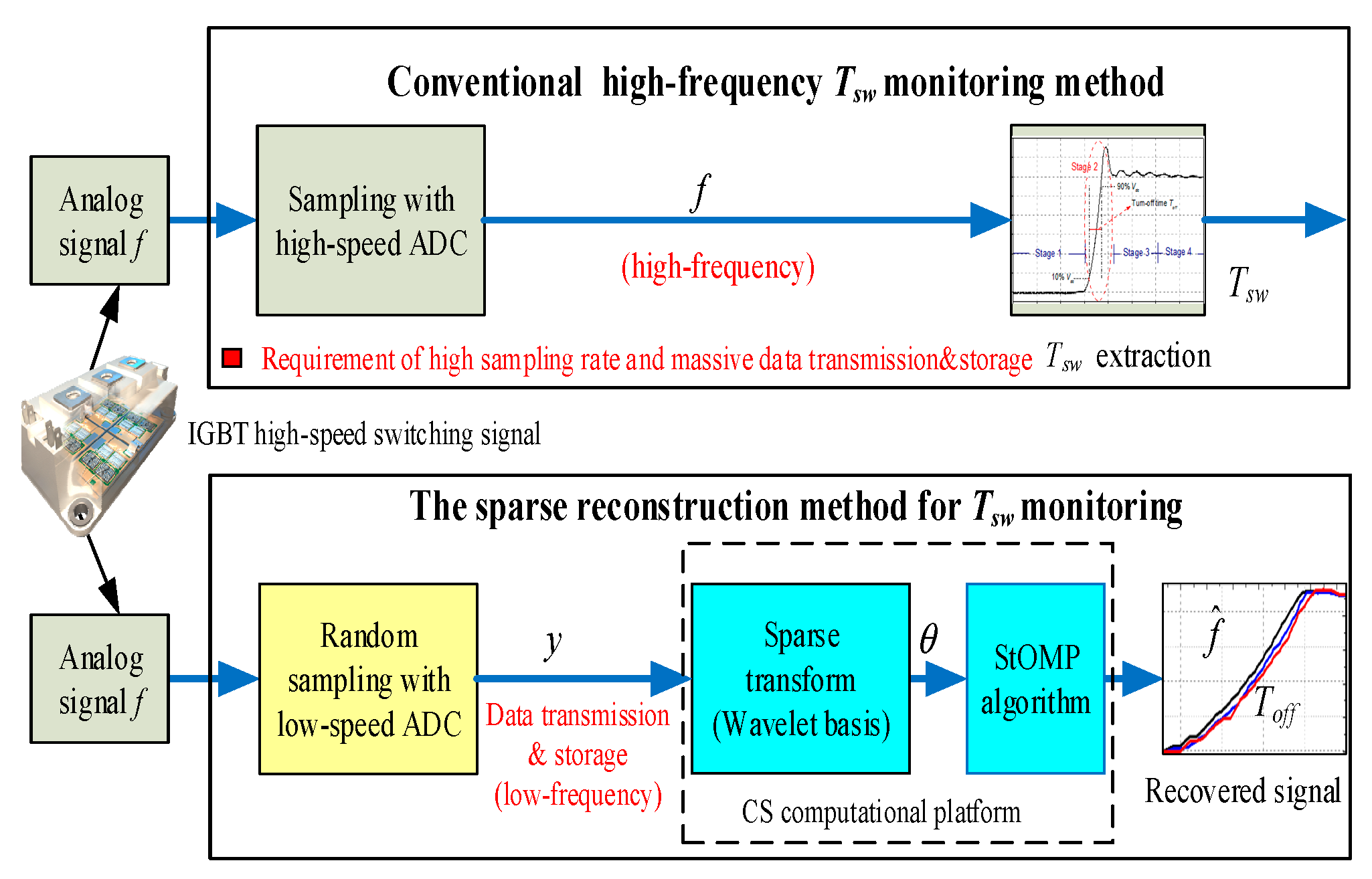
2. Under-Sampling Reconstruction Method for the IGBT Switching Signal

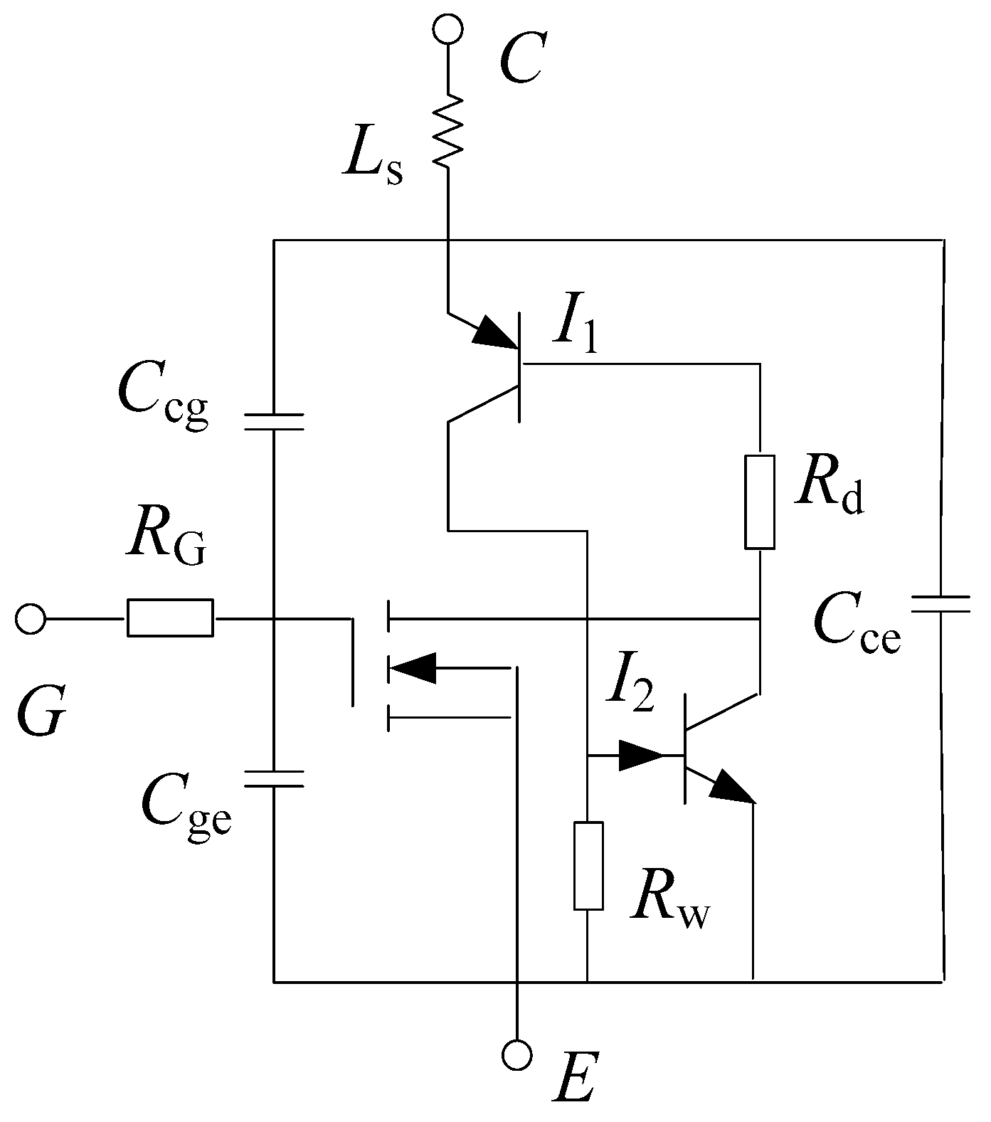
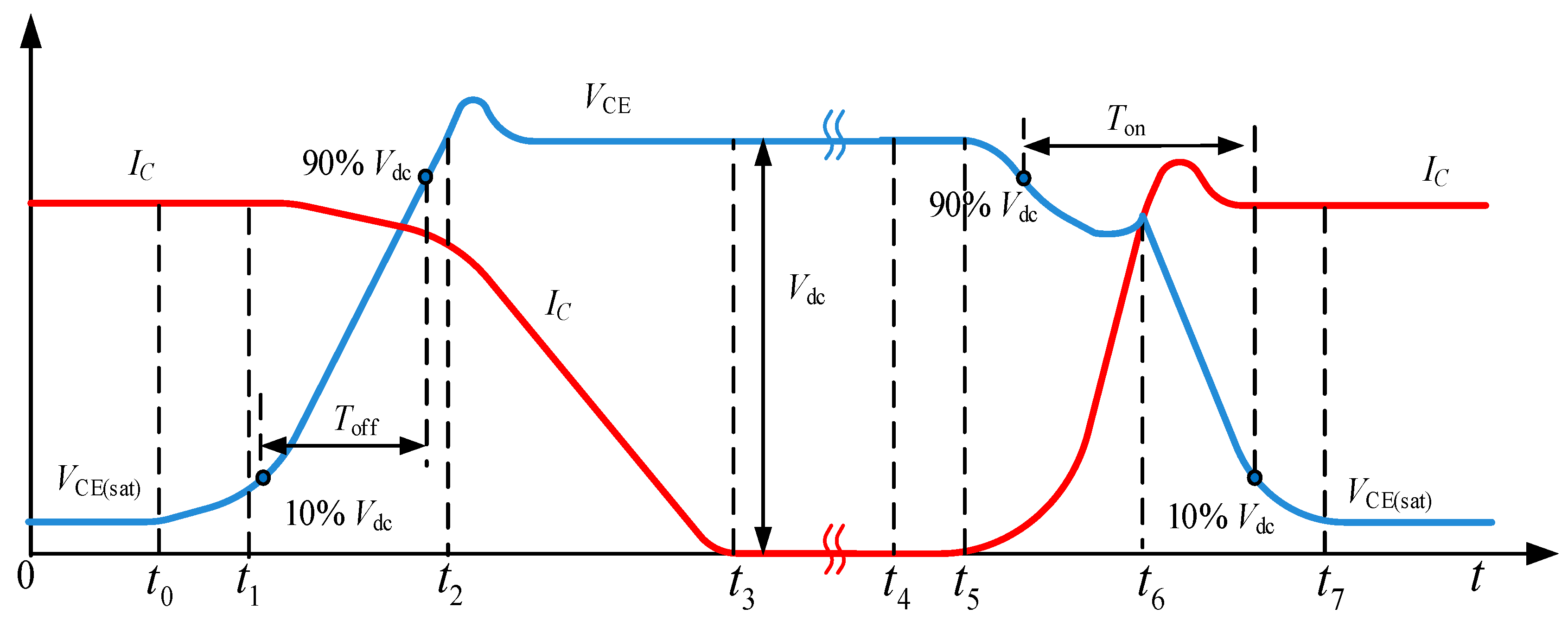
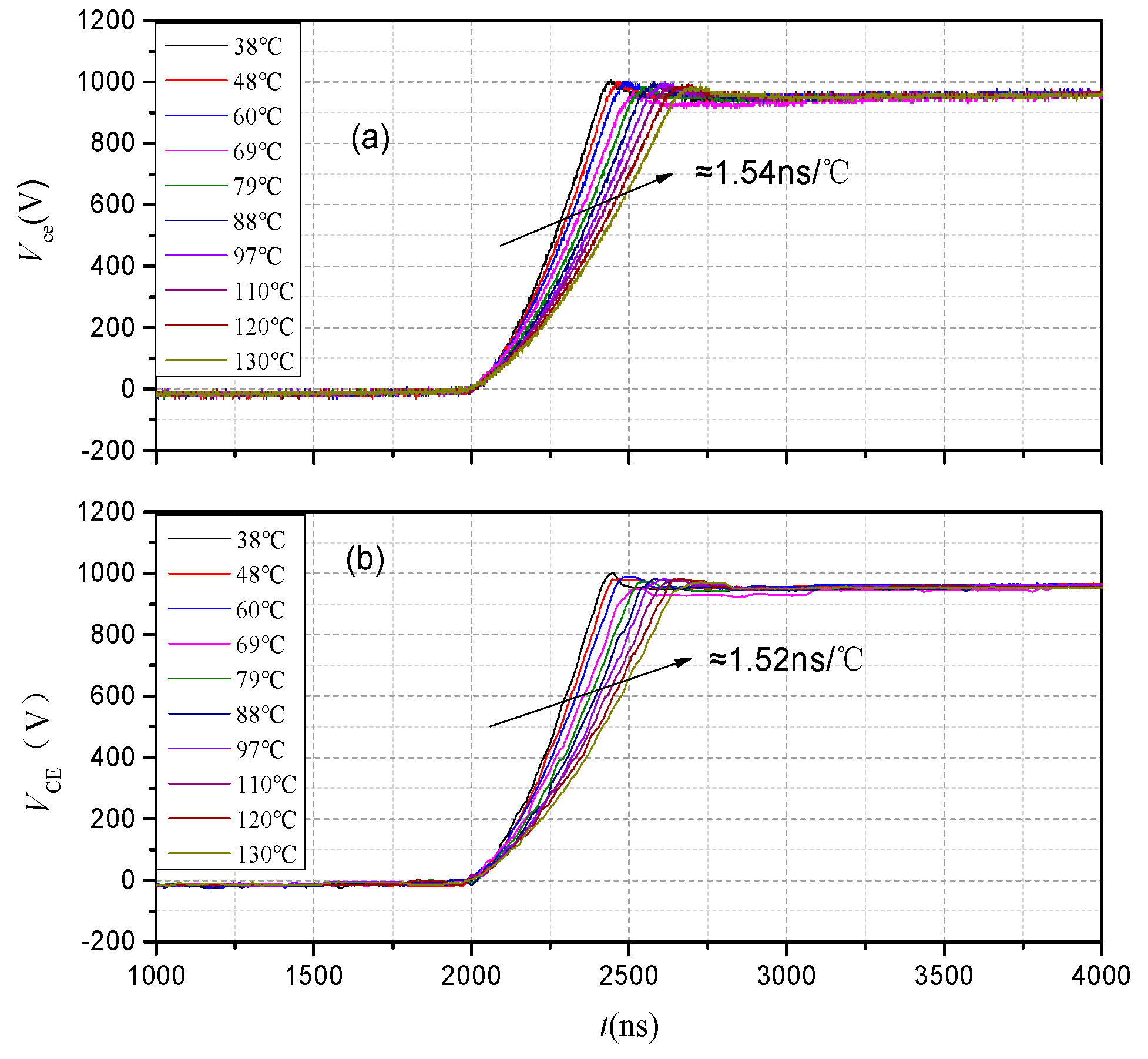
2.1. The Physical Mechanism behind the IGBT Switching Transitions

IGBT is a composite full-controlled power semiconductor device. The equivalent circuit of an IGBT is illustrated in Figure 1. Cge, Cgc, and Cce are the distributed capacitances among the gate-emitter, the gate-collector, and the collector-emitter, respectively. RG is the gate resistance, and Rd and Rw are the drift resistances of N and P regions, respectively, and inductance Ls represents the parasitic switching loop inductance. Taking the IGBT collector–emitter voltage VCE and the collector current IC into account, their waveforms during switching transitions (i.e., turn-on and turn-off) are shown in Figure 2. The physical mechanism behind IGBT switching transitions is described as follows:
1. IGBT Turn-off Transition
At the beginning time of turn-off transition, i.e., the turn-off voltage VGE is applied to the gate at t0, the Miller capacitor Cgc starts to charge, and the VCE rises slowly. The IC remains almost unchanged at the time period from t0 to t1 because the gate-emitter voltage VGE is still larger than the threshold voltage VTH. When Cgc reaches its steady state (VGE reaches VTH), VCE starts to rise rapidly at t1, and the change rate is determined by the carrier removal rate. The rapid rise of VCE causes IC to slowly fall at first. When VCE reaches the DC voltage Vdc at time t2, IC begins to fall rapidly. Due to the parasitic inductance in the circuit, an overshoot of VCE is induced. At t3, VCE maintains at Vdc, and IC has a small tail current. The change rate of VCE during IGBT turn-off transition is [17]:
d V CE d t = 1 τ G ( V g ( + ) V g ( ) 1 + ( C O / g m τ G ) ) ,
where τG = RGCgc, CO is the charge extraction capacitance, Vg(+) and Vg(-) are the on-state and off-state gate-emitter voltages, respectively, and gm is the transconductance. The change rate of IC in the t2-t3 phase is [18]:
d I c d t = g m V g V T I L / g m R g ( C gc + C ge ) + g m L s .
2. IGBT Turn-on Transition
At the beginning of IGBT turn-on transient under inductive load conditions, the gate voltage begins to rise at t4, and the gate current starts to charge Cgc and Cge. Once the gate-emitter voltage VGE is greater than the threshold voltage VT (at t5), the MOS channel starts to conduct (hole injection) and IC rises rapidly. The rising speed of IC is determined by RG and the behavior of MOS channel, which is expressed as:
d I c d t = g m ( V g + V T ) R g ( C gc + C ge ) + g m L s .
The initial fall of the collector voltage VCE appears due to the back electromotive force (EMF) across the stray inductance LS. The VCE falling speed is determined by LS and the change rate of IC. The load current communicates from the freewheeling diode to IGBT. When the IC reaches the load current IL (at t6), the freewheeling diode starts to turn off. Due to the reverse recovery current of the freewheeling diode, an overcurrent of IC will occur [18]. The stored charge within a diode is extracted, and the diode current falls below zero [19]. The collector voltage VCE may rise a little, like the concave shown in Figure 2. Then, VCE begins to drop rapidly to the saturation on-state voltage VCE (sat). The rate of VCE change at this stage is deduced as:
d V C E d t = 1 C g c [ V g + V T I L / g m R g + d I C d t ] .
As shown in Figure 2, the IGBT switching time Tsw (including the turn-on time Ton and the turn-off time Toff) are defined as the time durations of VCE decreasing from 90% to 10%, and increasing from 10% to 90% of its initial value, respectively. The IGBT switching time is related to current, junction temperature, and gate parameters. According to Equation (1), the increase of current will increase the carrier concentration, leading to a faster IGBT turn-off transition and thus a decrease of Toff. Moreover, with the increasing junction temperature, the carrier recombination becomes slower, leading to the increasing CO and Toff. Equation (4) shows that an increase of current would cause a slower rate of VCE change, which will result in an increase of Ton.
From the perspective of CM, the IGBT switching time is a reliable condition parameter that is related well to the health state of IGBT. For example, partial failure of a multichip device would change the switching time for a given current due to the changes in current density and stored charge of other healthy chips [2]. Other degradations such as solder fatigue and latch-up may also prolong the switching time of IGBT [4]. The Toff value is an early indicator to latch-up failure caused by damage in the die-attach layer [14]. On the other hand, the Ton can be also used a precursor of IGBT gate degradation [20].

2.2. Compressed Sensing of the IGBT Switching Signal

Switching time has been verified adequately to monitor the operational condition of the IGBT module [3,4,5], [10,11,12,13,14,15]. However, it requires a high-resolution and high accurate measurement of the small nanoseconds change during the fast switching transient. In practice, the conventional data acquisition (DAQ) with an extremely high sampling rate is very expensive with a heavy burden of data transmission, storage and computation. Compressed sensing is an emerging technique that allows sampling of analog signals at sub-Nyquist rates (i.e., the Shannon/Nyquist sampling theorem can be broken through) while avoiding the traditional issue of aliasing, and allowing for effective compression of signals during the sampling process [21].
According to the CS theory, a high-frequency VCE switching signal can be represented by a small amount of sampling points when expressed in terms of a proper basis. The basis in which a compressible signal is sparse is called a “sparsifying basis”. Sparse means that the signal has only a few non-zero elements. For an N-dimensional signal, if it has only K non-zero elements, it is K-sparse. As shown in Figure 2, the VCE during IGBT switching transitions is not sparse in the time domain. However, if there exists a transform basis such that the VCE switching signal is sparse in that transform basis, a low sampling rate can be performed by designing a suitable measurement matrix, and then the VCE switching signal can be recovered from a small number of sampling points.
The mathematical model for the sparse reconstruction method of IGBT high-speed switching signals is [22]:
y = Φ · f + e = Φ · Ψ · θ + e ,
where f is the original N × 1 dimension high-speed switching signal, y is the M × 1 dimension (M << N) sampling signal at a low sampling rate, e is a Gaussian white noise with dimension of N × 1, and Φ is a M × N dimension measurement matrix that is used to perform dimension-reduced projection of signal f to achieve compressed sampling. The premise of Equation (5) is that there exists an N × N-dimensional orthogonal transform base Ψ that can sparsely represent f, i.e., most components of the θ vector in f = Ψ·θ are zero. According to the theory of CS, the keys to recover the VCE switching signal from under-sampling data are: (1) the design of the measurement matrix Φ to obtain the under-sampling data y; (2) the selection of the orthogonal transform base Ψ to obtain the sparse representation θ of the switching signal; (3) and the utilization of the under-sampling data y to estimate the sparse vector θ and recover the original switching signal (f = Ψ·θ).
Since the dimension of the measurement signal y is much smaller than the dimension of the original signal f (M << N), the inverse problem of solving Equation (5) is actually an ill-posed problem, i.e., the original signal f cannot be directly estimated by M measurement values. According to the CS theory [23], in order to reconstruct the signal from a small amount of data, the sensing matrix A = Φ·Ψ needs to satisfy the Restricted Isometric Property (RIP) criteria, and the sparse basis Ψ must be irrelevant to the measurement matrix Φ. Considering the sparse property of vector θ (K non-zero terms), solving Equation (5) can be further transformed into a minimizing l0 norm problem, which can be expressed as:
{ θ ^ = arg   min θ 0 s . t . Φ · Ψ · θ = y ,
where ||θ||0 is the l0 norm, and Equation (6) is a complete NP-hard (non-deterministic polynomial) problem [21]. For a sparse signal, the l1 norm is the convex function closest to the l0 norm [24], and the minimum l1 norm and the minimum l0 norm have equivalent solutions. Therefore, the l1 linear programming algorithm can be used to solve the global optimal solution of the sparse vector θ, and the original VCE switching signal can be recovered from the under-sampling data by inverse transformation.

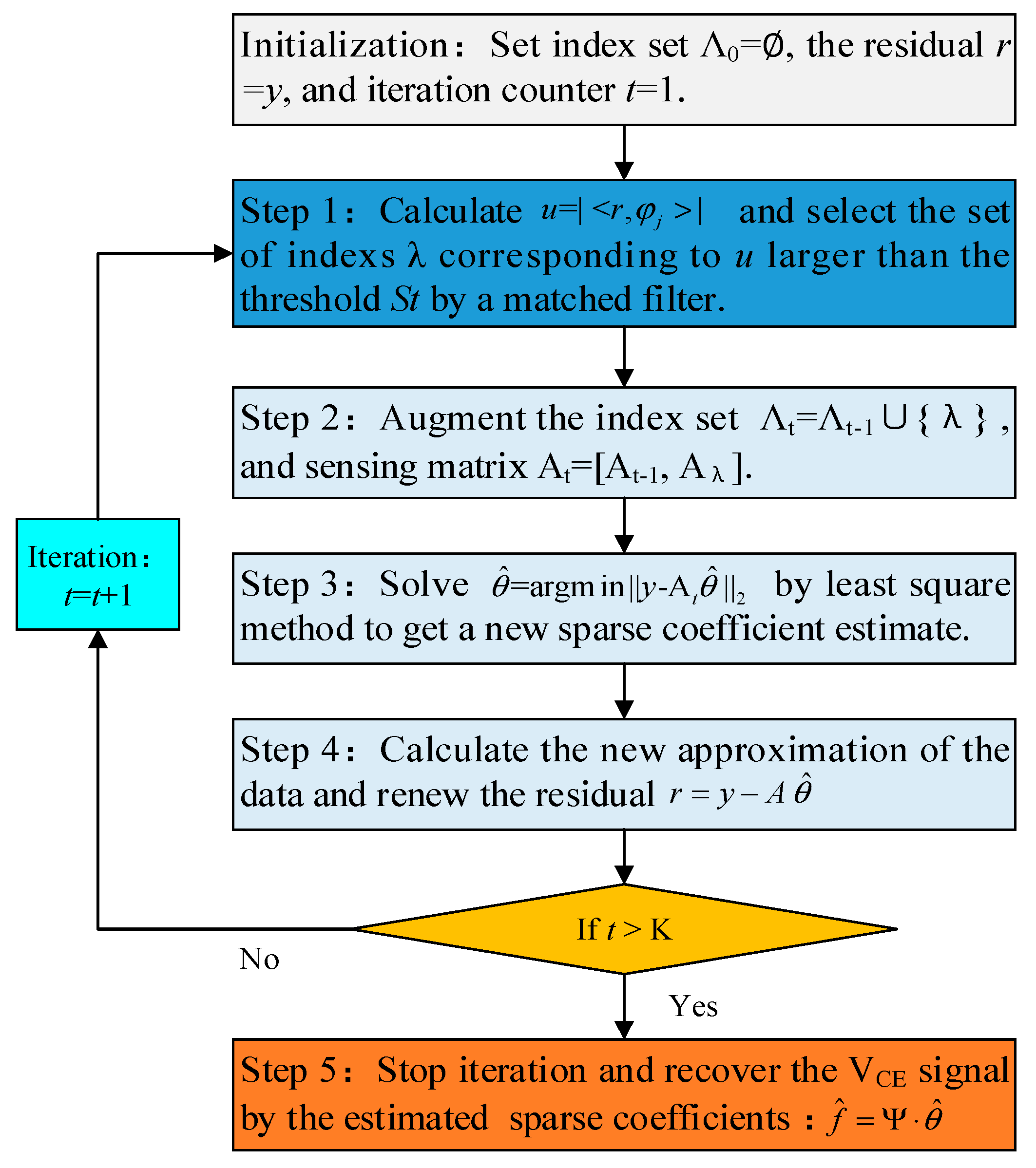
2.3. Sparse Reconstruction Algorithm

Figure 3 shows the schematic of the proposed CS based sparse reconstruction method for IGBT switching time monitoring with a reduced sampling rate. First, an N × M measurement matrix is constructed for random under-sampling of the IGBT high-speed switching signal VCE; in this way, the high-dimensional data are projected onto the low-dimensional space. The common used measurement matrices include Gaussian matrix, partial Hadamard matrix, and a random Bernoulli matrix [24], which meet both the RIP and irrelevance criteria. Then, the sparse basis is constructed to sparsely represent the high-dimensional VCE switching signal. Finally, the original VCE switching signal is recovered by using the reconstruction algorithm to extract the IGBT switching time.
As shown in Figure 2, the VCE switching signal has a multi-resolution feature, which can be decomposed into on/off steady state and on/off transient state. In the steady state, VCE is either the IGBT saturation voltage or the DC voltage Vdc, and the signal can be characterized as a DC component. The VCE transient state corresponds to the behavior of IGBT turn-on and/or turn-off transitions. As analyzed in Section 2.1, the characteristics of the VCE switching transition signal are related to the distribution parameters of IGBT module. To accurately identify the nanoseconds IGBT switching time, it is required to sparsely represent the switching transient characteristics of VCE signal, i.e., VCE signal is transformed and projected onto an orthogonal transform base. The wavelet transform consists of different spatial resolution, frequency and directional characteristics, which defines a well-sparse representation of signal transients and singularities. Previous study in [24] showed that the wavelet basis could sparsely represent the IGBT switching transient signal more effectively than the Fourier basis. Similarly, this paper uses the Mallat algorithm to construct an N × N Haar wavelet basis to sparsely represent the VCE signal [25].
The reconstruction algorithm is vital for IGBT switching time monitoring, which recovers the high-dimensional signal from the under-sampling data. As analyzed in Section 2.2, the essence of sparse reconstruction of VCE signal is a sparse decomposition process of compressing measurement data on redundant dictionaries [23]. For the orthogonal matching pursuit algorithm (OMP), the local optimal solution is selected based on greedy iteration to gradually approximate the original signal, so that the original VCE signal can be reconstructed with a high probability, as applied in previous study [25]. However, the OMP algorithm will introduce new computation overheads during the Schmidt orthogonalization, and only one atom is selected in each iteration to update the support set. If the amount of data is large, the iteration efficiency may be low or even the reconstruction may be failed. Considering the IGBT switching frequency in a real power converter is generally from a few kHz to several tens of kHz, there are numerous switching transitions in a fundamental period with massive CM data. The computation time of the reconstruction algorithm for processing the massive data is important for online monitoring. Different from using the OMP algorithm in [24], the Stagewise Orthogonal Matching Pursuit (StOMP) algorithm is used to improve the efficiency and reduce the computation time for VCE switching signal reconstruction [25]. The flowchart of the StOMP algorithm to reconstruct the VCE switching signal is presented in Figure 4.
The basic steps of the StOMP algorithm are similar to the OMP algorithm, such as matching atoms by maximizing the residual inner product and updating the residual by minimizing the residual norm. However, unlike the OMP algorithm, in which only one optimal solution element is selected per iteration, the StOMP algorithm forms a matched filter by setting a threshold and selects all atoms with a residual inner product greater than the threshold St in each iteration, thus reducing the matching pursuit times and speeding up the convergence of the algorithm [25].

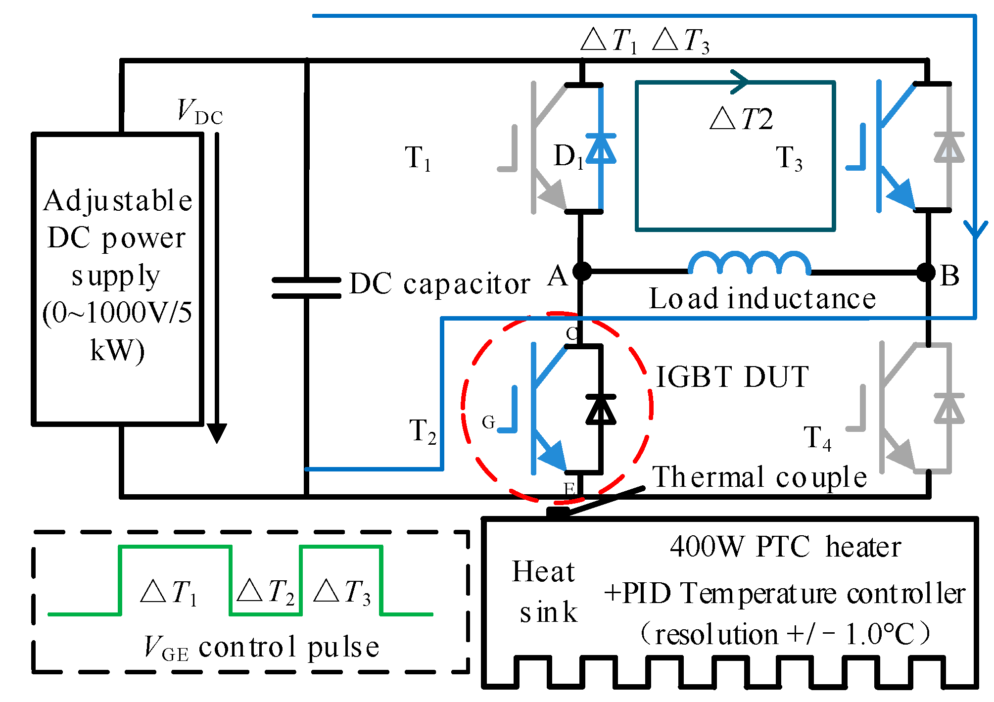
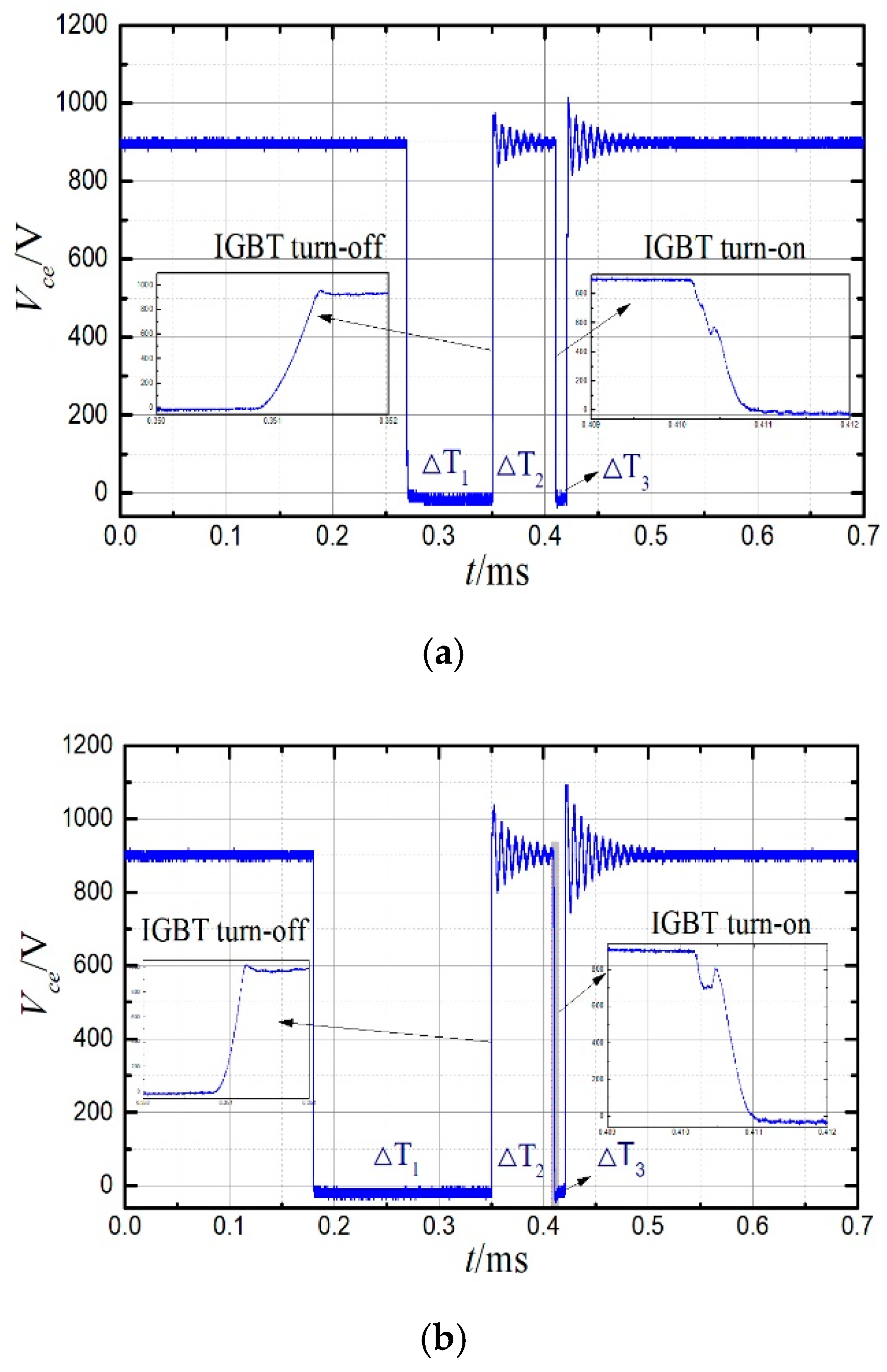
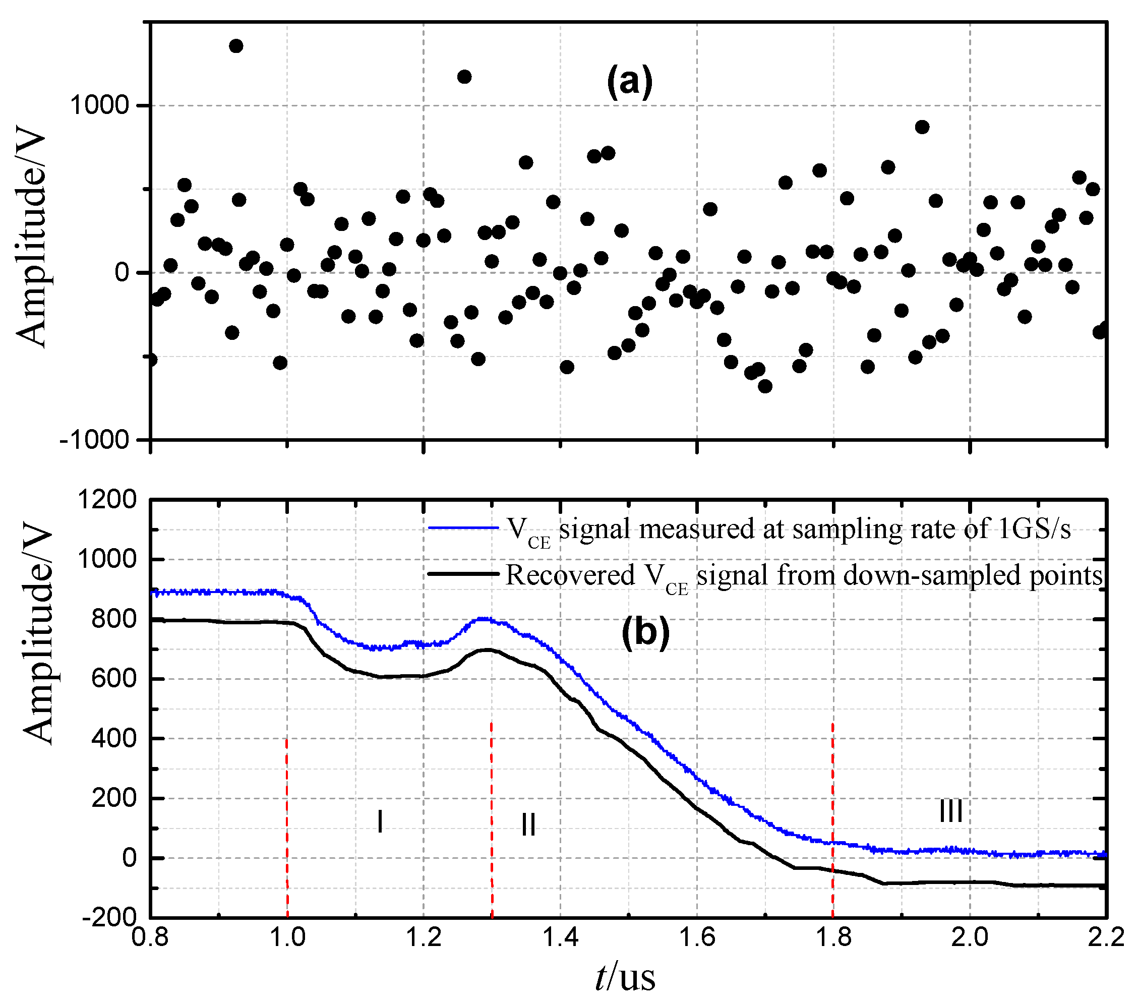
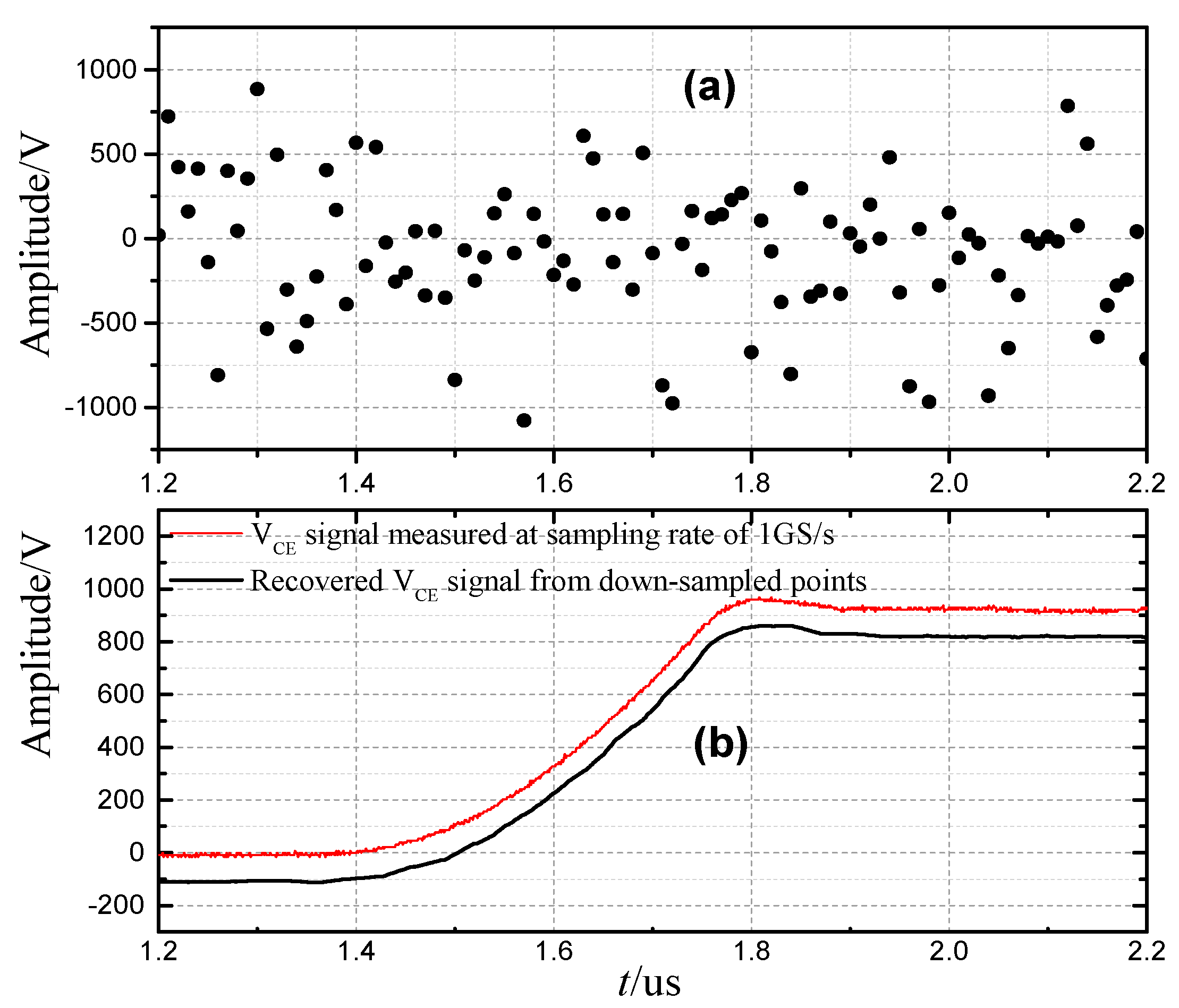
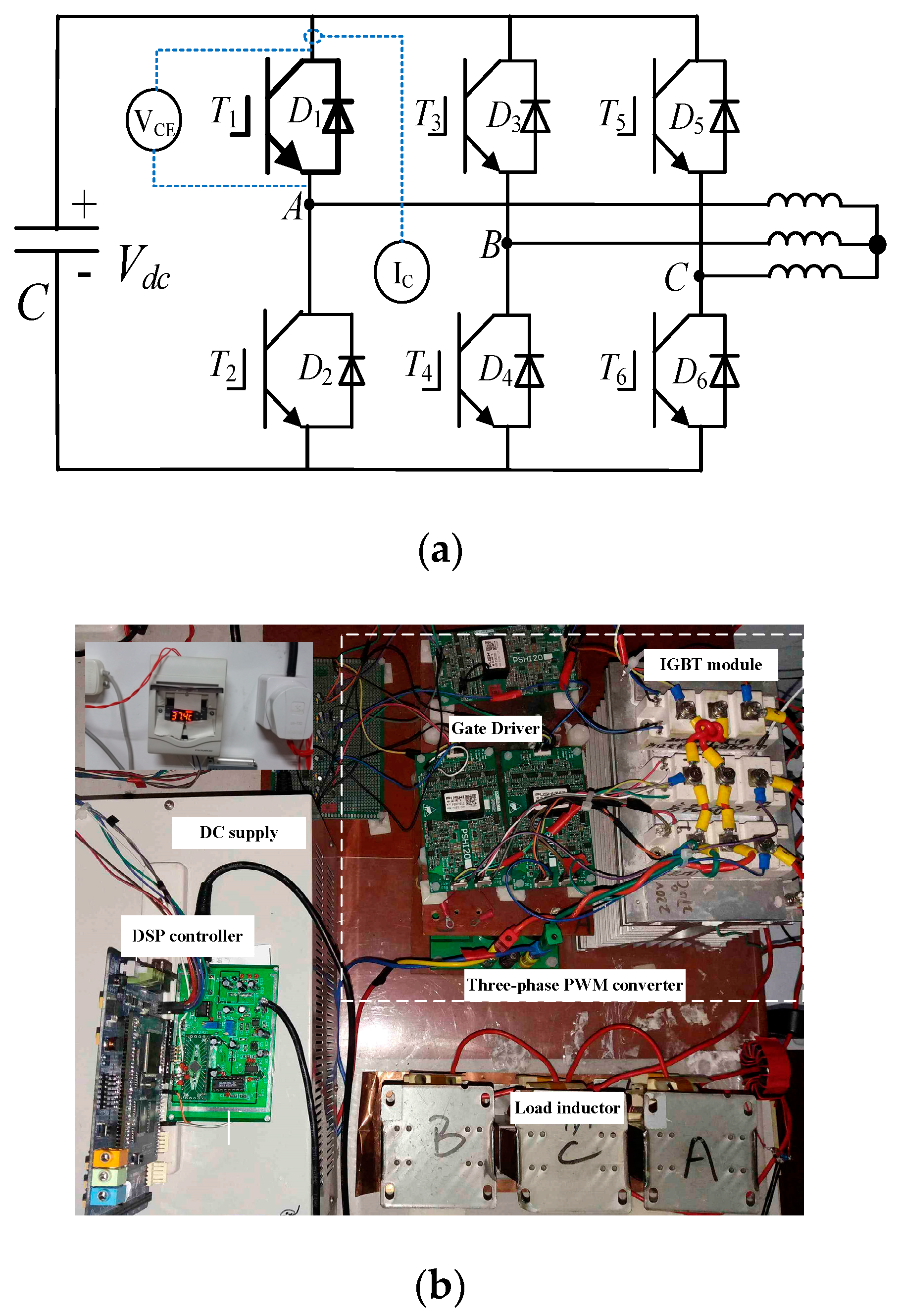
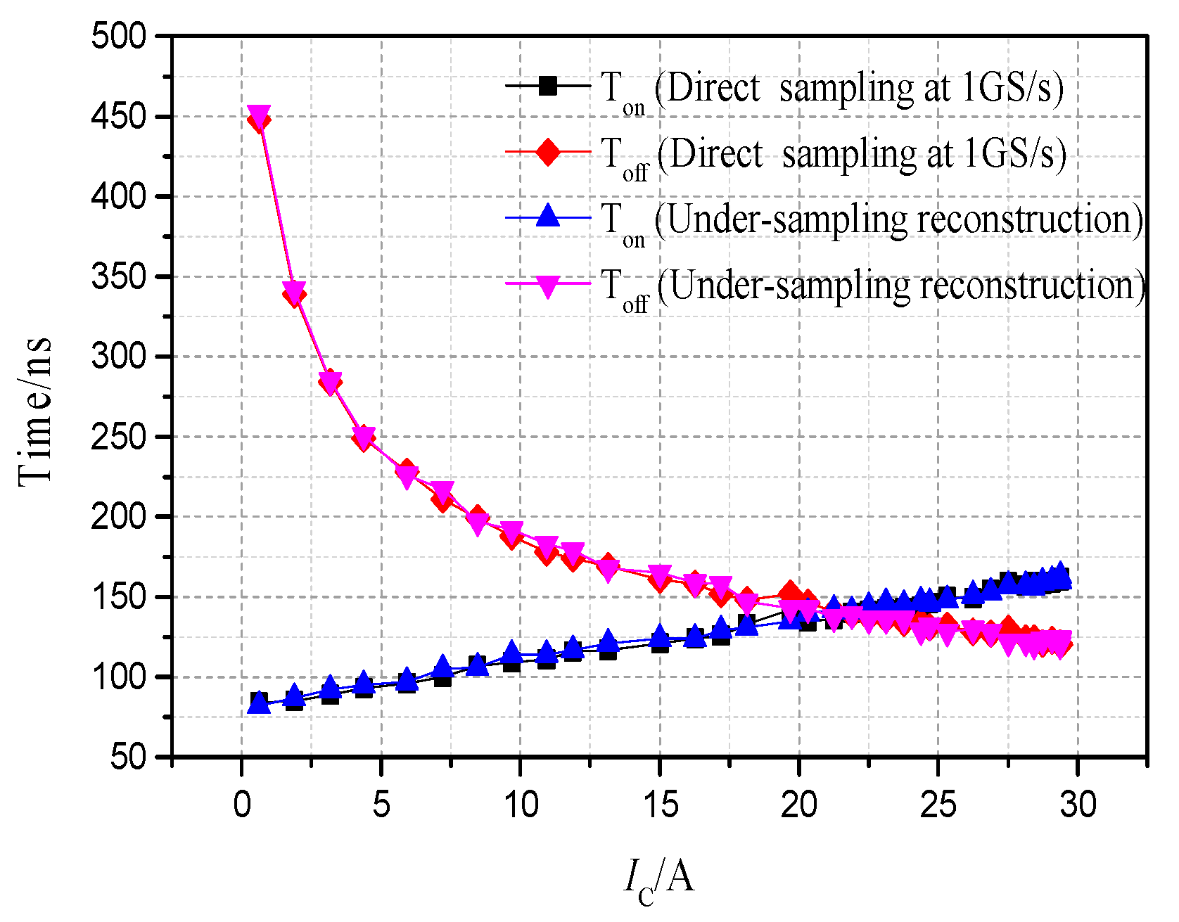
3. Experimental Verification

3.1. Double-Pulse Tests

To verify the feasibility and effectiveness of the proposed sparse reconstruction method for IGBT switching time monitoring, the IGBT double-pulse test is implemented first. The schematic diagram of the H-bridge based double-pulse test rig is shown in Figure 5. The adjustable DC power supply is used to regulate the DC voltage (0–1000 V). The DSP controller (TI, F28335) is used for IGBT switching control. A heating system consisting of a PTC heater and a PID temperature controller is applied to regulate temperature of the IGBT. The IGBT case temperature is measured by a thermal couple with an accuracy of 1 °C. The parameters of the IGBT double-pulse test rig are in accordance with [24]. The device under test (DUT) is an Infineon IGBT module [26] FF450R17ME4 (1.7 kV/450 A) and the load inductance is 2.2 mH.
The IGBT can be controlled at any preset voltage, current, and temperature by using the test rig. Taking the IGBT T2 as an example of DUT, the IGBT T1 and IGBT T4 are controlled turn off during the double-pulse test, while the IGBT T3 is controlled turn-on. During the time period of ΔT1, the DC capacitor starts to charge the load inductor through T3 and T2. The magnitude of the collector current is determined by the pulse width of ΔT1. The collector current increases with the ΔT1. During ΔT2, T2 is turned off, and the load current continues to flow through the anti-parallel diode D1 and the IGBT T3. If the load inductance is large enough, the load current changes slowly and remains stable. Therefore, the IGBT T2 can be controlled turned-on and turn-off under different load currents by controlling the pulse width of ΔT1. Figure 6 shows the VCE waveform of T2 measured by a differential voltage probe with a sampling rate of 1 GS/s, when the load current is 100 A and 200 A, respectively. It can be seen that the VCE waveform during IGBT turn-on transition has an obvious concave characteristic in the decreasing process, which agrees well with the theoretical analysis in Section 2.1.
Figure 7a and Figure 8a show the under-sampling points during IGBT turn-on and turn-off transitions, respectively. From these under-sampling points, the VCE switching transitions signals are recovered by the proposed sparse reconstruction method, as shown in Figure 7b and Figure 8b, respectively. The compression ratio of sampling rate is 10. To evaluate the performance of signal reconstruction, the recovered VCE transient signals are compared with the original VCE signal at a sampling rate of 1 GS/s. For comparison, a 100 V vertical shift is inserted intentionally between the recovered and reconstructed VCE signals. From the experimental results, the difference between the reconstructed VCE signal and the original VCE signal is very small. The specific characteristics of the IGBT switching signal can be recovered well with a largely reduced sampling rate (10-fold). As shown in Figure 7b and Figure 8b, the concave and overshoot behaviors of the VCE signal during IGBT turn-on and turn-off transitions are well characterized by the proposed sparse reconstruction method.
To quantify the percent error between the original VCE signal f and the recovered VCE signal fr, the reconstruction error Ce is defined as [27]:
C e = f - f r 2 f 2 · 100 % .
Different random measurement matrices including Gauss matrix, Bernoulli matrix, and a partial Hadamard matrix are used to the VCE switching signal and the statistical results of the reconstruction error are listed in Table 1. The VCE reconstruction error during IGBT turn-off is less than 1%. The VCE turn-on reconstruction errors using the random Gauss matrix and the random Bernoulli matrix are less than 1.5%. The VCE turn-on reconstruction error is slightly larger than of the turn-off—that is, because the characteristics of VCE waveform during IGBT turn-on are more complex [17,18]. As shown in Figure 7, the VCE waveform has three transient stages during IGBT turn-on process. In the first stage, VCE is decreased by the voltage drop of stray inductance during the fast rising of IC. In the second stage, the freewheeling diode sustains a reverse voltage and VCE rises a little and then drops quickly as the depletion layer shrinks toward the drift region. In the third stage, VCE decays slowly because the carrier diffusion velocity in the drift (base) region is less than the disappearance velocity of depletion layer. In addition, the StOMP algorithm used in this work and the OMP algorithm used in [23] are tested under the same conditions. The StOMP algorithm has a faster reconstruction speed than the OMP algorithm, and the computation time of the VCE signal by the StOMP algorithm is 0.32 ms when compared with 2.89 ms by the OMP algorithm.
As described in Section 2.2, the temperature affects the recombination velocity of the carriers, thereby affecting the IGBT turn-off time. The IGBT case temperature is controlled by the PID temperature controller, and the switching times are monitored under thermal equilibrium conditions. Figure 9 shows the VCE turn-off signal in the temperatures range of 38–130 °C. It is found that the IGBT turn-off time increases with temperature. This is because the carrier in the space charge region is removed from the depletion layer at a slower rate as the junction temperature and the charge extraction capacitor increases. As a result, the IGBT turn-off speed becomes slower. The temperature-sensitive coefficient of the turn-off time calculated by the least squares fitting method under direct high-frequency sampling is about 1.54 ns/°C. For the proposed sparse reconstruction method, the derived temperature sensitivity is about 1.52 ns/°C. In the experiment, the measurement error of IGBT turn-off time is less than 2 ns at different temperatures. Such an accuracy is adequate for the switching time based IGBT junction temperature estimation.

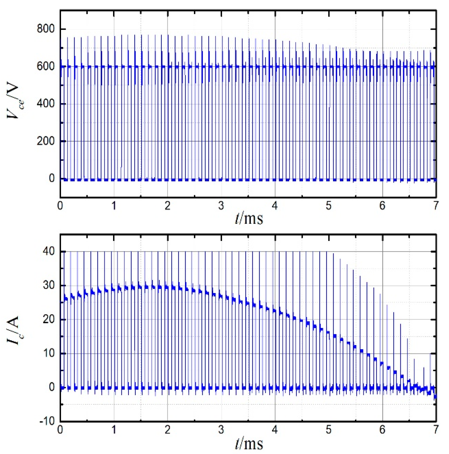
3.2. PWM Converter Test

As analyzed in Section 2.1, the IGBT switching time varies with the instantaneous current (since the carrier concentration speed is different [16]). The proposed sparse reconstruction method is further verified in a three-phase PWM converter. The schematic diagram and picture of the PWM converter test rig are shown in Figure 10. The tested IGBT module is Infineon IGBT module FF50R12RT4 (1200 V/50 A) (Neubiberg, Germany) [26]. The DC voltage is 600 V, and the load inductance is 8 mH/phase. The fundamental frequency of the PWM converter is 50 Hz with a peak current of 30 A, while the switching frequency of IGBT is 8 kHz. Figure 11 shows the experimental waveforms of VCE and IC. The IGBT switching time at different IC (0–30 A) are extracted by the direct high sampling rate method and the proposed under-sampling reconstruction method, respectively. The comparative results are exhibited in Figure 12.
It can be clearly seen that the IGBT switching time changes with the instantaneous current. With the increasing instantaneous current, the IGBT turn-off time (Toff) decreases while the IGBT turn-on time (Ton) increases. When the value of IC is very small, the IGBT turn-on speed is faster than the turn-off speed. Ton is 84 ns and Toff is 448 ns when IC = 0.63 A. When IC = 21.9 A, Ton and Toff tend to be the same value of ca. 140 ns. The extracted IGBT switching time by the proposed sparse reconstruction method is close to the direct high sampling rate method (the average error is less than 2 ns). Experimental results demonstrate that the under-sampling reconstruction method could reflect the IGBT nanoseconds switching time variation at a 10-fold reduction of sampling rate. For the purpose of fault prognosis, the change of switching time at a certain current and case temperature can be used to reflect the health status of IGBT [13,14,15]. The potential applications of the proposed method for IGBT junction temperature measurement will be further studied.

4. Conclusions

To overcome the technical difficulty of the extremely high sampling rate for IGBT nanoseconds switching time online monitoring, this paper proposes a CS based under-sampling reconstruction monitoring method. By analyzing the physical mechanism behind the IGBT switching transitions, the VCE switching signal is sparsely represented by the wavelet basis, and the StOMP algorithm is proposed to recover the high-speed VCE signal for under-sampling data. Finally, experimental verification is conducted on not only the double-pulse test, but also a real PWM converter. The results show that:
(1) The characteristics of VCE signal during switching transitions can be recovered from the under-sampling data with a reconstruction error less than 2%. The StOMP algorithm shows a faster convergence speed than the traditional OMP algorithm for sparse reconstruction.
(2) The under-sampling reconstruction method can monitor the nanoseconds change of IGBT switching time variation with a largely reduced sampling rate. At a compressed ratio 10 of the sampling rate, the detection accuracy of less than 2 ns can be achieved.

Author Contributions

Conceptualization, H.L.; methodology, H.L.; validation, M.Z. and H.Y.; investigation, X.Y.; writing—original draft preparation, H.L.

Funding

This work was funded in part by the National Natural Science Foundation of China (NSFC) under Grant No. 51907116, and Shanghai Science and Technology Innovation Action under Grant No. 19DZ1205402 and Shanghai Green Energy Grid Connected Technology Engineering Research Center: No. 13DZ2251900.

Conflicts of Interest

The authors declare no conflict of interest.

References

  1. Habetler, T.G.; Harley, R.G. Power electronic converter and system control. Proc. IEEE 2001, 89, 913–925. [Google Scholar] [CrossRef]
  2. Yang, S.; Bryant, A.; Mawby, P.; Xiang, D.; Ran, L.; Tavner, P. An Industry-Based Survey of Reliability in Power Electronic Converters. IEEE Trans. Ind. Appl. 2011, 47, 1441–1451. [Google Scholar] [CrossRef] [Green Version]
  3. Yang, S.; Xiang, D.; Bryant, A.; Mawby, P.; Ran, L.; Tavner, P. Condition Monitoring for Device Reliability in Power Electronic Converters: A Review. IEEE Trans. Power Electron. 2010, 25, 2734–2752. [Google Scholar] [CrossRef]
  4. Oh, H.; Han, B.; McCluskey, P.; Han, C.; Youn, B.D. Physics-of-Failure, Condition Monitoring, and Prognostics of Insulated Gate Bipolar Transistor Modules: A Review. IEEE Trans. Power Electron. 2015, 30, 2413–2426. [Google Scholar] [CrossRef]
  5. Wang, B. Review of Power Semiconductor Device Reliability for Power Converters. CPSS Trans. Power Electron. Appl. 2017, 2, 101–117. [Google Scholar] [CrossRef]
  6. Xiang, X.; Ran, L.; Tavner, P.; Yang, S.; Bryant, A.; Mawby, P. Condition monitoring power module solder fatigue using inverter harmonic identification. IEEE Trans. Power Electron. 2012, 27, 235–247. [Google Scholar] [CrossRef]
  7. Avenas, Y.; Dupont, L.; Khatir, Z. Temperature Measurement of Power Semiconductor Devices by Thermo-Sensitive Electrical Parameters—A Review. IEEE Trans. Power Electron. 2012, 27, 3081–3092. [Google Scholar] [CrossRef]
  8. Ma, K.; He, N.; Liserre, M.; Blaabjerg, F. Frequency-Domain Thermal Modeling and Characterization of Power Semiconductor Devices. IEEE Trans. Power Electron. 2016, 31, 7183–7193. [Google Scholar] [CrossRef]
  9. Pedersen, K.B.; Pedersen, K. Dynamic Modeling Method of Electro-Thermo-Mechanical Degradation in IGBT Modules. IEEE Trans. Power Electron. 2016, 31, 975–986. [Google Scholar] [CrossRef]
  10. Luo, H.; Chen, Y.; Sun, P.; Li, W.; He, X. Junction Temperature Extraction Approach With Turn-Off Delay Time for High-Voltage High-Power IGBT Modules. IEEE Trans. Power Electron. 2016, 31, 5122–5132. [Google Scholar] [CrossRef]
  11. Luo, H.; Li, W.; Iannuzzo, F.; He, X.; Blaabjerg, F. Enabling Junction Temperature Estimation via Collector-Side Thermo-Sensitive Electrical Parameters Through Emitter Stray Inductance in High-Power IGBT Modules. IEEE Trans. Ind. Electron. 2018, 65, 4724–4738. [Google Scholar] [CrossRef]
  12. Bahman, A.S.; Ma, K.; Ghimire, P.; Iannuzzo, F.; Blaabjerg, F. A 3-D-Lumped Thermal Network Model for Long-Term Load Profiles Analysis in High-Power IGBT Modules. IEEE J. Emerging Sel. Top. Power Electron. 2016, 4, 1050–1063. [Google Scholar] [CrossRef] [Green Version]
  13. Zhou, S.; Zhou, L.; Sun, P. Monitoring Potential Defects in an IGBT Module Based on Dynamic Changes of the Gate Current. IEEE Trans. Power Electron. 2013, 28, 1479–1487. [Google Scholar] [CrossRef]
  14. Brown, D.W.; Abbas, M.; Ginart, A.; Ali, I.N.; Kalgren, P.W.; Vachtsevanos, G.J. Turn-Off Time as an Early Indicator of Insulated Gate Bipolar Transistor Latch-up. IEEE Trans. Power Electron. 2012, 27, 479–489. [Google Scholar] [CrossRef]
  15. Patil, N.; Celaya, J.; Das, D.; Goebel, K.; Pecht, M. Precursor Parameter Identification for Insulated Gate Bipolar Transistor (IGBT) Prognostics. IEEE Trans. Reliab. 2019, 58, 271–276. [Google Scholar] [CrossRef]
  16. Denk, M.; Bakran, M.-M. Comparison of UCE- and RGi-based junction temperature measurement of multichip IGBT power modules. In Proceedings of the 2015 17th European Conference on Power Electronics and Applications (EPE’15 ECCE-Europe), Geneva, Switzerland, 8–10 September 2015. [Google Scholar]
  17. Bryant, A.; Yang, S.; Mawby, P.; Xiang, D.; Ran, L.; Tavner, P.; Palmer, P.R. Investigation Into IGBT dV/dt During Turn-Off and Its Temperature Dependence. IEEE Trans. Power Electron. 2011, 26, 3019–3031. [Google Scholar] [CrossRef] [Green Version]
  18. Feng, H.; Yang, W.; Onozawa, Y.; Yoshimura, T.; Tamenori, A.; Sin, J.K.O. Transient Turn-ON Characteristics of the Fin p-Body IGBT. IEEE Trans. Electron Devices 2015, 62, 2555–2561. [Google Scholar] [CrossRef]
  19. Bryant, A.T.; Lu, L.; Santi, E.; Hudgins, J.L.; Palmer, P.R. Modeling of IGBT Resistive and Inductive Turn-On Behavior. IEEE Trans. Ind. Appl. 2008, 44, 904–914. [Google Scholar] [CrossRef]
  20. Chen, L.; Peng, F.Z.; Cao, D. A smart gate drive with self-diagnosis for power MOSFETs and IGBTs. In Proceedings of the 2008 Twenty-Third Annual IEEE Applied Power Electronics Conference and Exposition, Austin, TX, USA, 24–28 February 2008. [Google Scholar]
  21. Li, H.; Xiang, D.; Yang, X.; Zhang, X. Compressed Sensing Method for IGBT High-Speed Switching Time On-Line Monitoring. IEEE Trans. Ind. Electron. 2019, 66, 3185–3195. [Google Scholar] [CrossRef]
  22. Donoho, D.L. Compressed sensing. IEEE Trans. Inf. Theory 2006, 52, 1289–1306. [Google Scholar] [CrossRef]
  23. Donoho, D.L. For most large underdetermined systems of linear equations the minimal 𝓁1-norm solution is also the sparsest solution. Commun. Pure Appl. Math. 2006, 59, 797–829. [Google Scholar] [CrossRef]
  24. Craven, D.; McGinley, B.; Kilmartin, L.; Glavin, M.; Jones, E. Compressed Sensing for Bioelectric Signals: A Review. IEEE J. Biomed. Health Inf. 2015, 19, 529–540. [Google Scholar] [CrossRef] [PubMed]
  25. Donoho, D.; Tsaig, Y.; Drori, I.; Starck, J. Sparse Solution of Underdetermined Systems of Linear Equations by Stagewise Orthogonal Matching Pursuit. IEEE Trans. Inf. Theory 2012, 58, 1094–1121. [Google Scholar] [CrossRef]
  26. Website of Infineon. Available online: https://www.infineon.com/ (accessed on 18 September 2019).
  27. Mesnil, O.; Ruzzene, M. Sparse wavefield reconstruction and source detection using Compressed Sensing. Ultrasonics 2016, 67, 97–104. [Google Scholar] [CrossRef]
Figure 1. Equivalent circuit of IGBT.
Electronics 08 01203 g001
Figure 2. Waveforms of VCE and IC during IGBT switching transitions.
Electronics 08 01203 g002
Figure 3. The propose sparse reconstruction method of IGBT switching signal for CM.
Electronics 08 01203 g003
Figure 4. Flowchart of the StOMP algorithm for reconstruction of VCE signal.
Electronics 08 01203 g004
Figure 5. Schematic of the IGBT double-pulse test rig.
Electronics 08 01203 g005
Figure 6. Experimental waveforms of VCE in double-pulse test: (a) IC = 100 A; (b) IC = 200 A.
Electronics 08 01203 g006
Figure 7. Reconstruction of VCE signal during IGBT turn-on transition: (a) random under-sampling points (100 MS/s); (b) comparison of the recovered VCE signal and original VCE signal.
Electronics 08 01203 g007
Figure 8. Reconstruction of VCE signal during IGBT turn-off transition: (a) random under-sampling points (100 MS/s); (b) comparison of the recovered VCE signal and original VCE signal.
Electronics 08 01203 g008
Figure 9. IGBT turn-off transitions under different case temperatures: (a) direct sampling at sampling rate of 1GS/s; (b) sparse reconstruction.
Electronics 08 01203 g009
Figure 10. The PWM converter test for IGBT switching time monitoring: (a) schematic diagram; (b) picture of test rig.
Electronics 08 01203 g010
Figure 11. Experimental waveforms of VCE and IC in the PWM converter test.
Electronics 08 01203 g011
Figure 12. Ton and Toff with different IC.
Electronics 08 01203 g012
Table 1. The reconstruction error of IGBT switching signal with different measurement matrices.
Random Measurement MatrixReconstruction Error e
Gauss matrix1.35%0.76%
Bernoulli matrix1.22%0.85%
Partial Hadamard matrix2.01%0.77%

