Article

A Comprehensive Comparison of EMI Immunity in CMOS Amplifier Topologies

Department of Information Engineering, University of Brescia, 25121 Brescia BS, Italy
*
Author to whom correspondence should be addressed.
Electronics 2019, 8(10), 1181; https://doi.org/10.3390/electronics8101181
Submission received: 10 September 2019 / Revised: 8 October 2019 / Accepted: 15 October 2019 / Published: 17 October 2019
(This article belongs to the Special Issue Low-Voltage Integrated Circuits Design and Application)

Abstract

:
This paper provides the results of a comprehensive comparison between complementary metal oxide semiconductor (CMOS) amplifiers with low susceptibility to electromagnetic interference (EMI). They represent the state-of-the-art in low EMI susceptibility design. An exhaustive scenario for EMI pollution has been considered: the injected interference can indeed directly reach the amplifier pins or can be coupled from the printed circuit board (PCB) ground. This is also a key point for evaluating the susceptibility from EMI coupled to the output pin. All of the amplifiers are re-designed in a United Microelectronics Corporation (UMC) 180 nm CMOS process in order to have a fair comparison. The topologies investigated and compared are basically derived from the Miller and the folded cascode ones, which are well-known and widely used by CMOS analog designers.

1. Introduction

Electromagnetic interference (EMI) can be injected on an arbitrary pin of an integrated circuit (IC). The interfering signal can propagate through the various active devices composing the IC. If the EMI level is very high, exceeding the supply rails, the electrostatic discharge (ESD) protective circuitry will trigger. Instead, in the case of smaller EMI signals, the latter will be distorted since all active devices are essentially non-linear. This distortion will generate in-band spurious signals and even an EMI-induced DC shift of the voltage at the circuit nodes, which is very harmful for the proper operation of the analog circuits. The problem is very critical because the possible sources of interference (natural, artificial, and among them, voluntary or not) are practically everywhere. Moreover, the ubiquitousness of electronics (in control systems, in biomedical devices, in automotive products,...) requires a high safety level and, therefore, robustness to interference.
Several studies are reported in the literature that describe the EMI susceptibility of analog ICs, [1,2,3,4,5,6,7,8,9,10,11]; it has been modeled and verified with simulations and experiments [12,13,14,15]. These works also consider very high frequencies [12,13,14], or are based on neural networks [13]. Moreover, most of them focus on the operational amplifiers because of their high sensitivity to EMI and because they are the main building blocks in analog designs [1,2,3,4,5,6,7,8,9,10,11].
Recently, it has been stated that the scenario for EMI pollution can be simplified in two cases: the classic one in which the interference is directly injected into the pins of the inputs and of the power supply; and the newest, in which the EMIs are also coupled from the printed circuit board (PCB) ground plane and, consequently, the output pin can also be a point of injection [16,17]. In practical PCB designs, indeed, the ground plane is commonly shared with other analog, digital, or mixed-signal circuits and ICs, which can be a source of high-frequency signals and, therefore, of interference. Regarding the classic scenario, several studies have investigated opamp susceptibility, and many various topologies with a better EMI immunity have been presented in recent years [18,19,20,21,22]. Instead, with regard to the second scenario, research is only beginning, and the main result is the measurement of the susceptibility of commercial devices to the interferences capacitively coupled to the ouput pin [16,17].
The aim of this paper is a fair comparison between the state-of-the-art complementary metal oxide semiconductor (CMOS) amplifiers in the low EMI susceptibility design, considering the full EMI scenario with several points of EMI injection. Miller and folded cascode topologies are considered because they are well-known and widely used among the CMOS amplifiers. The analysis starts from the basic architectures, then the improved topologies are investigated in the full EMI pollution scenario. All of the amplifiers are re-designed in a United Microelectronics Corporation (UMC) 180 nm CMOS process in order to have a fair comparison, and the simulations are performed on the netlist extracted from the layout view.
The Miller amplifiers are considered and compared in terms of AC parameters and EMI immunity in Section 2. In Section 3, the same is done for the folded cascode topologies, and in Section 4, the result of the comparison is discussed and conclusions are drawn.

2. CMOS Miller Amplifiers

2.1. Compared Topologies and Their AC Characteristics

The CMOS Miller amplifier is based on the cascade connection of a differential input stage and a common source stage. Being a two-stage topology, it exhibits a medium-high gain and the largest output voltage swing, but it needs frequency compensation and also usually exhibits a large asymmetry of the positive and negative slew rate. Here, a standard Miller amplifier is designed in the UMC 180 nm CMOS process, with an nmos differential pair biased with a current of 100 μ A, 1.8 V of voltage supply. The sizing of the transistors is chosen to have a gain of about 60 dB and a gain bandwidth (GBW) larger than 10 MHz. The classic Miller topology is compared to the source-buffered (SB) Miller amplifier proposed in [18] with improved robustness against EMI and is shown in Figure 1 for the sake of clarity. In addition, the SB amplifier is designed in UMC technology and is sized to have AC characteristics similar to that of the standard Miller amplifier. The final AC parameters of both the classic and the SB Miller amplifiers are listed in Table 1, while the aspect ratio of the transistors is listed in Table 2. As one can see, they are approximately the same. Indeed, the source-buffered amplifier is different from the classic one only by the addition of a network biasing the bulk of the differential pair and the addition of a couple of filter capacitances at the inputs. Due to the fact that the input stage is the most critical for the interferences, this small difference between the circuits actually has a strong impact on the immunity to the EMI injected into the input non-inverting pin, as stated and measured in the literature [18,23,24].

2.2. Susceptibility to EMI sDirectly Injected

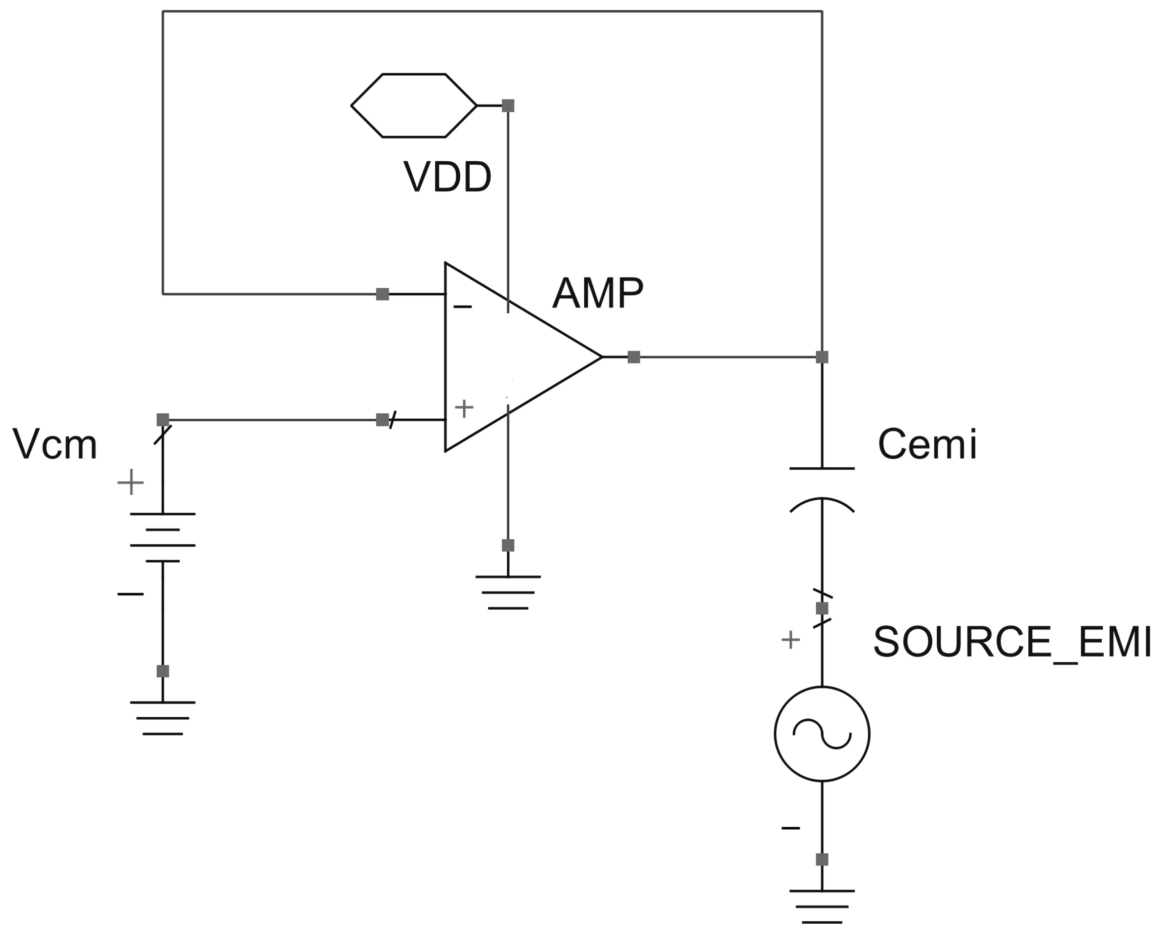
In order to compare their EMI susceptibility, both of the amplifiers are measured in the configuration represented in Figure 2 and following a method well-known in the literature. The amplifiers are therefore in the voltage follower configuration, and the offset of the output voltage intuitively quantifies the susceptibility to interferences.
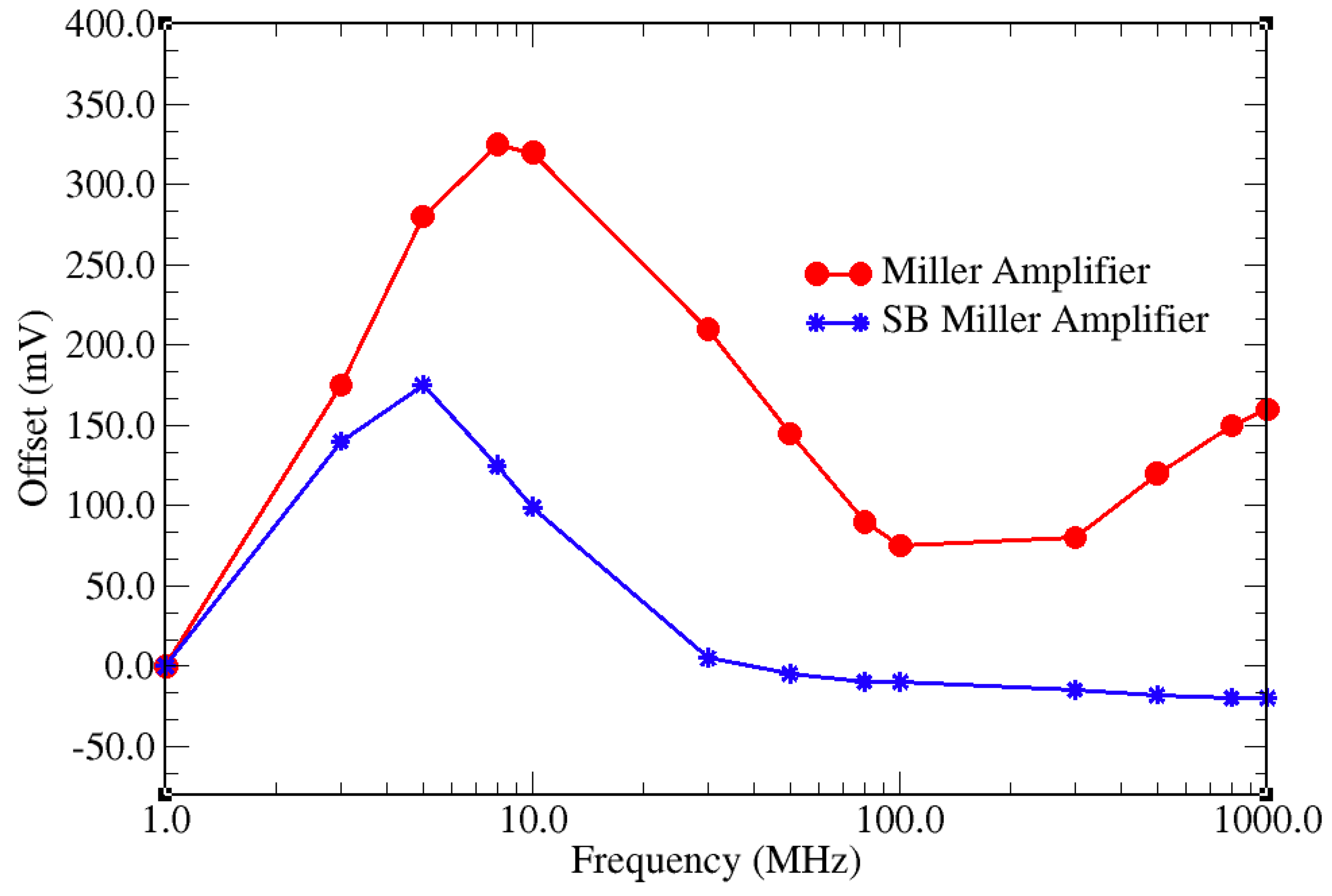
With regard to the EMIs directly injected, they have been deeply investigated in the literature. For this reason, we plot only the offset caused by the interferences injected into the non-inverting pin: it is known, indeed, as the worst case. The peak-to-peak amplitude of the interfering signal is equal to half of Vdd (900 mV); its frequency ranges between 1 MHz and 1 GHz. The offset resulting from injecting the EMI is plotted in Figure 3.
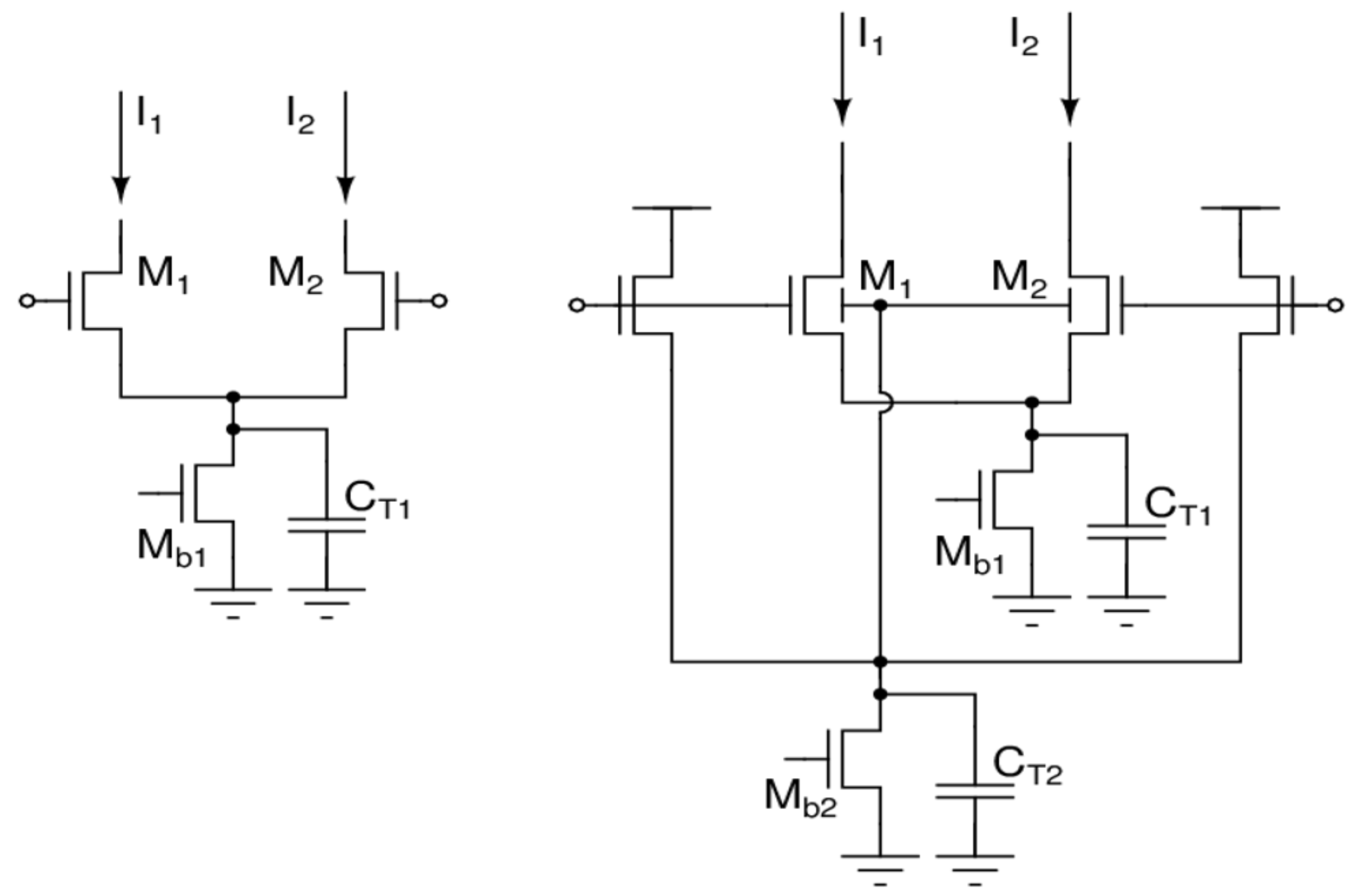
The classic Miller amplifier exhibits a remarkable susceptibility also at medium frequency due to its asymmetry, which is intuitive considering the difference between its positive and negative slew rate. Instead, as expected, the SB Miller amplifier exhibits a much smaller offset. The SB Miller amplifier indeed reduces the parasitic tail capacitor, which shunts the tail current source ( C T 1 ) and shorts the latter at high EMI frequencies. This tail capacitor is mostly composed of the bulk-to-source capacitors of the input pair, which is heavily reduced by the source-buffered topology. For the sake of clarity, the classic and the source-buffered differential pair is shown in Figure 4. Moreover, it is worth remembering that in [18], a couple of filter capacitors were added to further increase the EMI immunity at very high frequencies.

2.3. Susceptibility to EMI Coupled from the Ground Plane

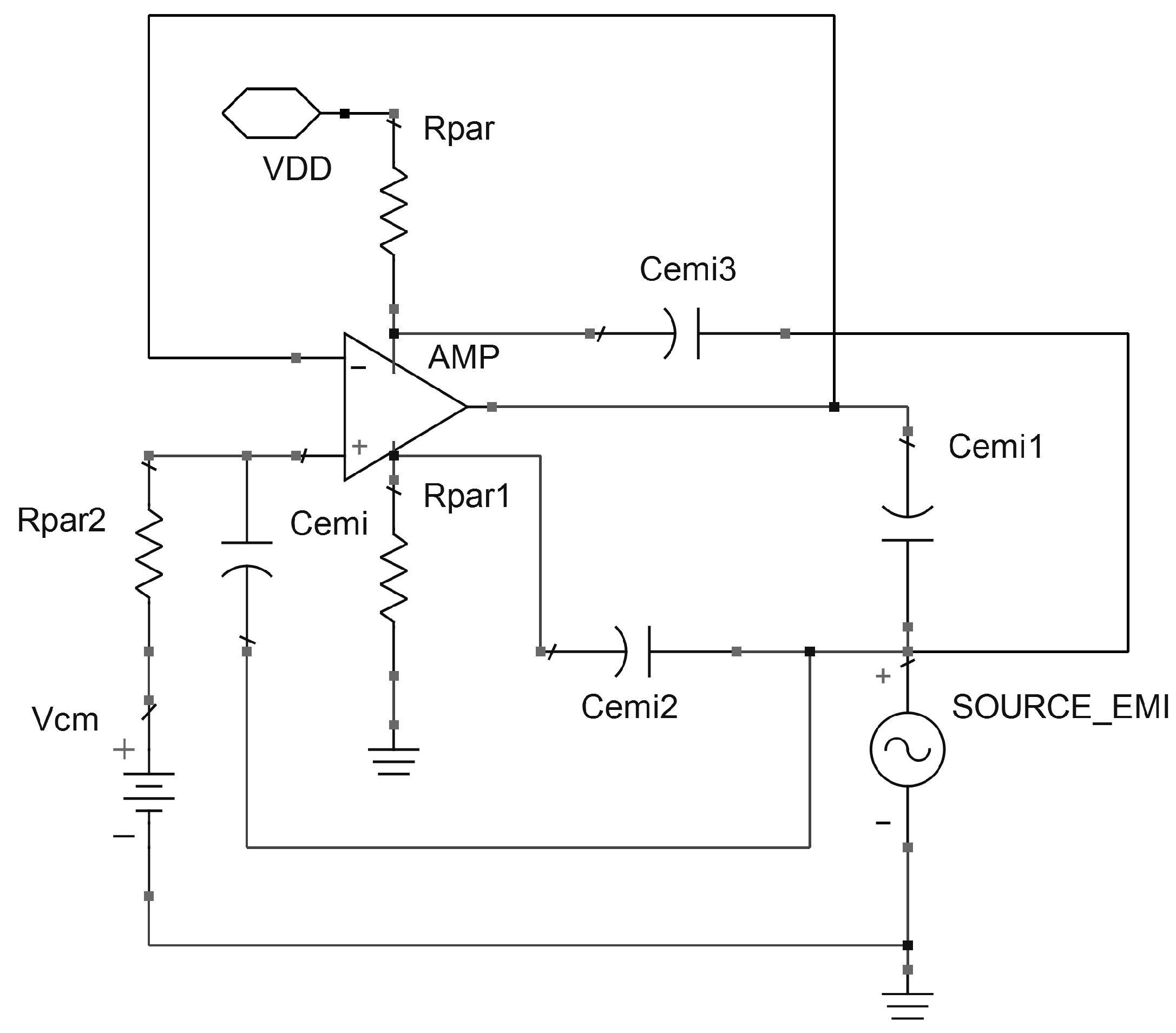
The next step is to compare the behavior of the Miller amplifiers in the case of noise arising from the ground plane. This is a novel scenario much less investigated in the literature. Therefore, we consider two particular conditions: the interferences coupled only to the output pin and the interferences coupled to all of the pins of the IC being tested. These configurations are represented in Figure 5 and Figure 6, respectively. The value of the capacitors that represent the parasitics of the board is of 4.7 pF; the parasitic series resistances must be added in the schematic, otherwise the voltage would be fixed by the ideal voltage source without EMI (for example, Vdd).
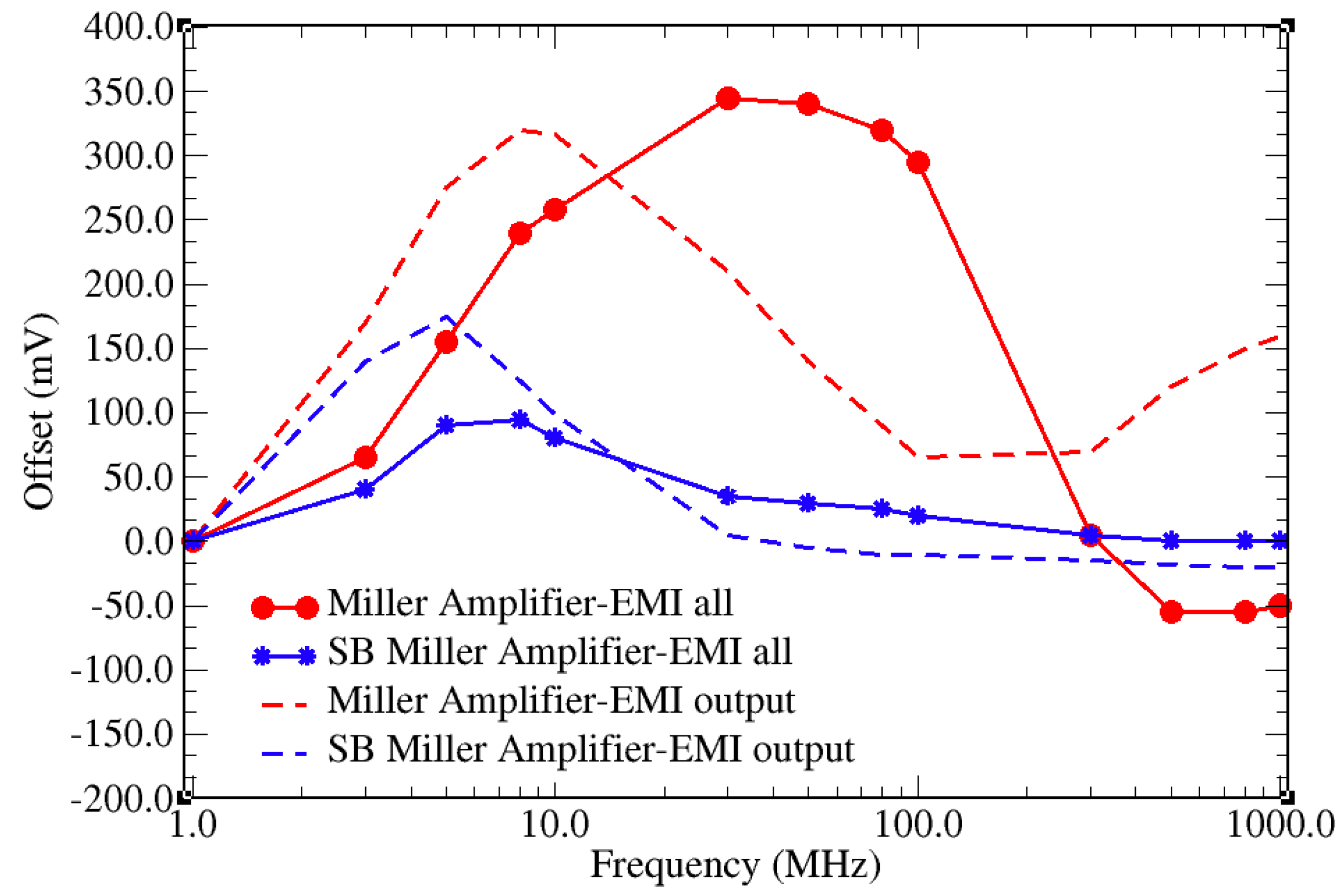
In Figure 7, the offset induced by the EMI coupled from the ground plane is plotted. The solid lines represent the offset in the case of EMI coupled to all of the pins, while the dashed lines plot the offset in the case of EMI coupled only to the output pin.
From the plots, one can see that the SB Miller amplifier exhibits a better immunity not only to the EMI injected into the input pin but also to the EMI coupled to the output pin and, more generally, to all of the pins. At first look, this result could be a little surprising because the second stage of the SB amplifier is exactly the same as the classic amplifier, but we must consider the feedback loop. The amplifiers are indeed connected in the voltage follower configuration, and therefore, the noise picked up from the output pin is also fed back to the input stage.Another interesting consideration is that the ouput pin is a critical point of injection: most of the offset is indeed induced by the interferences coupled only from the output pin. Finally, at medium frequencies, the offset induced by EMI coupled from the ground plane is rather predictable because it is similar to that induced by EMI direct injection into the non-inverting input pin. Instead, at very high frequencies, the offset can even change the sign and it is no longer predictable.

3. Folded Cascode Amplifiers

Compared Topologies and Their AC Characteristics

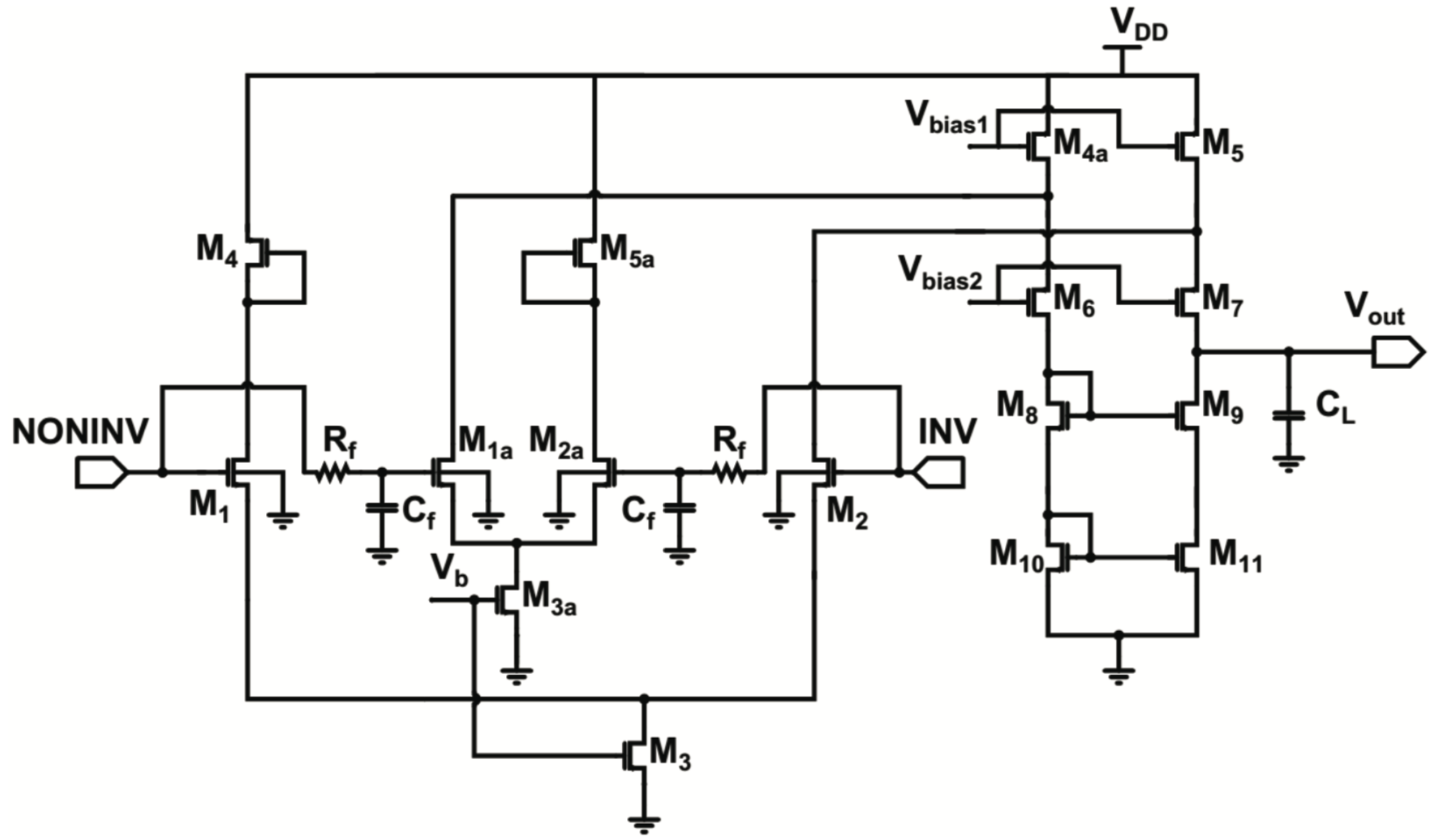
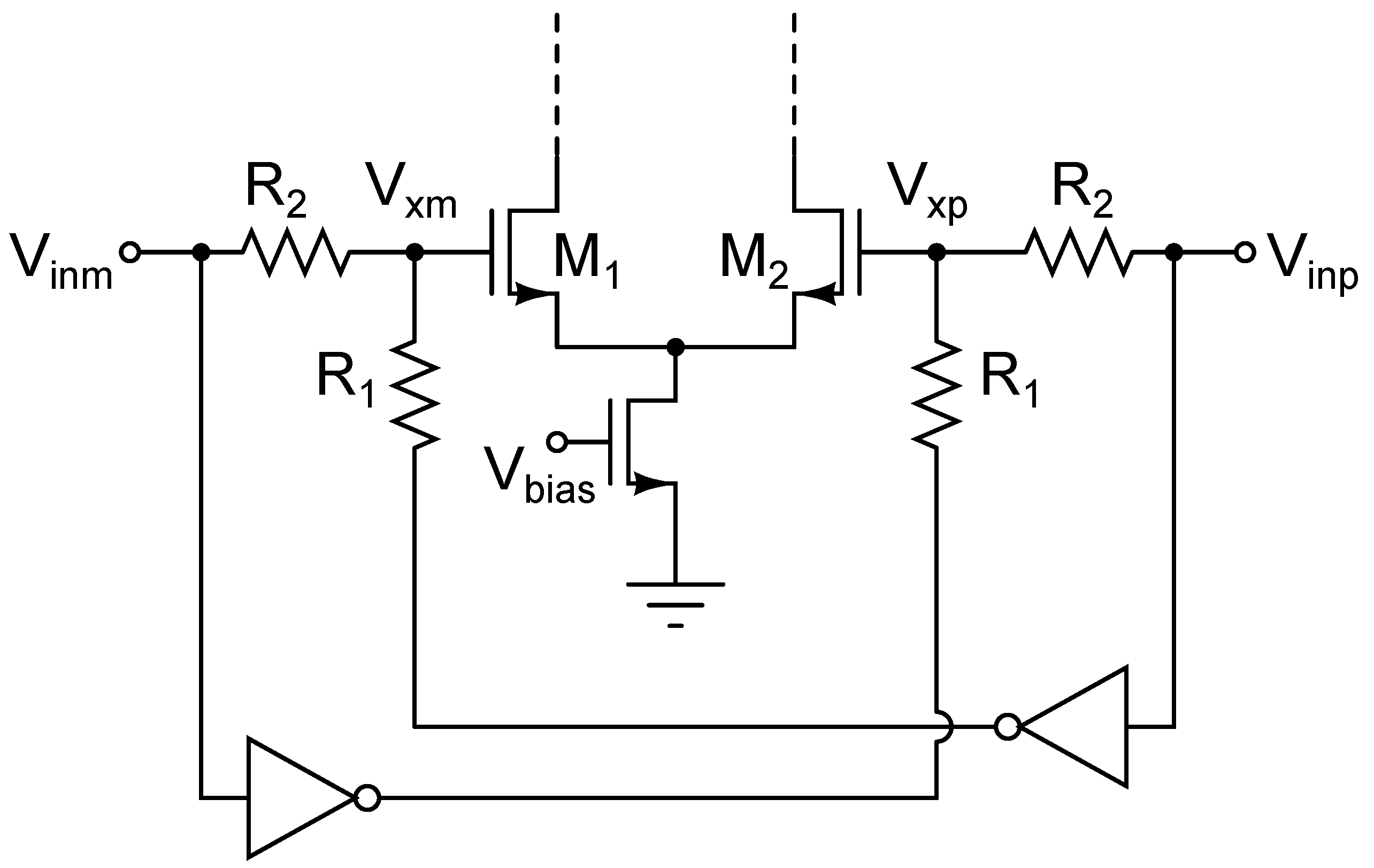
The folded cascode (FC) amplifier is another widely used topology. It is a single-stage amplifier, achieving a large gain by using cascode load. This means that the folded cascode does not need the frequency compensation, and therefore, it usually exhibits a larger bandwidth. On the other hand, the output swing is thus limited by the cascode loads. From the classic FC topology, several other circuits have been proposed in the literature, aiming to increase its EMI immunity. It is worth adding that the folded cascode exhibits a more symmetrical behavior with respect to the Miller amplifier, and then its susceptibility mostly happens only at high frequencies. Adding an RC (resistor–capacitor) filter seems, therefore, to be the easy way to achieve a good immunity in the FC amplifier. However, a straightforward use of an RC filter is impractical because it deteriorates the phase margin and, therefore, the stability of the amplifier. A better solution is based on the RC filter connected to a replica input stage, as suggested in [19,25]; the latter topology is shown in Figure 8. Another topology, robust to EMI, is the source buffered folded cascode, which is based on a input differential pair similar to that of the SB Miller amplifier. This topology can be further improved by adding the replica input stage with its RC filter, as proposed in [19] and shown in Figure 9. Finally, another different solution is obtained by adding a common-mode cancellation circuit (CMCC) to the classic FC amplifier [21,22]. For the sake of clarity, the CMCC is shown in Figure 10.
All of these architectures exhibit an improved immunity to the interfering signals, and they represent the state-of-the-art. As a next step they are, therefore, designed in the UMC 180 nm process with 3.3 V of voltage supply and similar design goals (in terms of gain, GBW, power consumption, and so on) to have a fair comparison. The final AC parameters of the classic FC, the FC with replica circuit shown in Figure 8, the improved SB folded cascode amplifier in Figure 9, and the FC amplifier plus the CMCC are listed in Table 3.
Moreover, the aspect ratio of the transistors composing the folded cascode architectures are listed in Table 4.
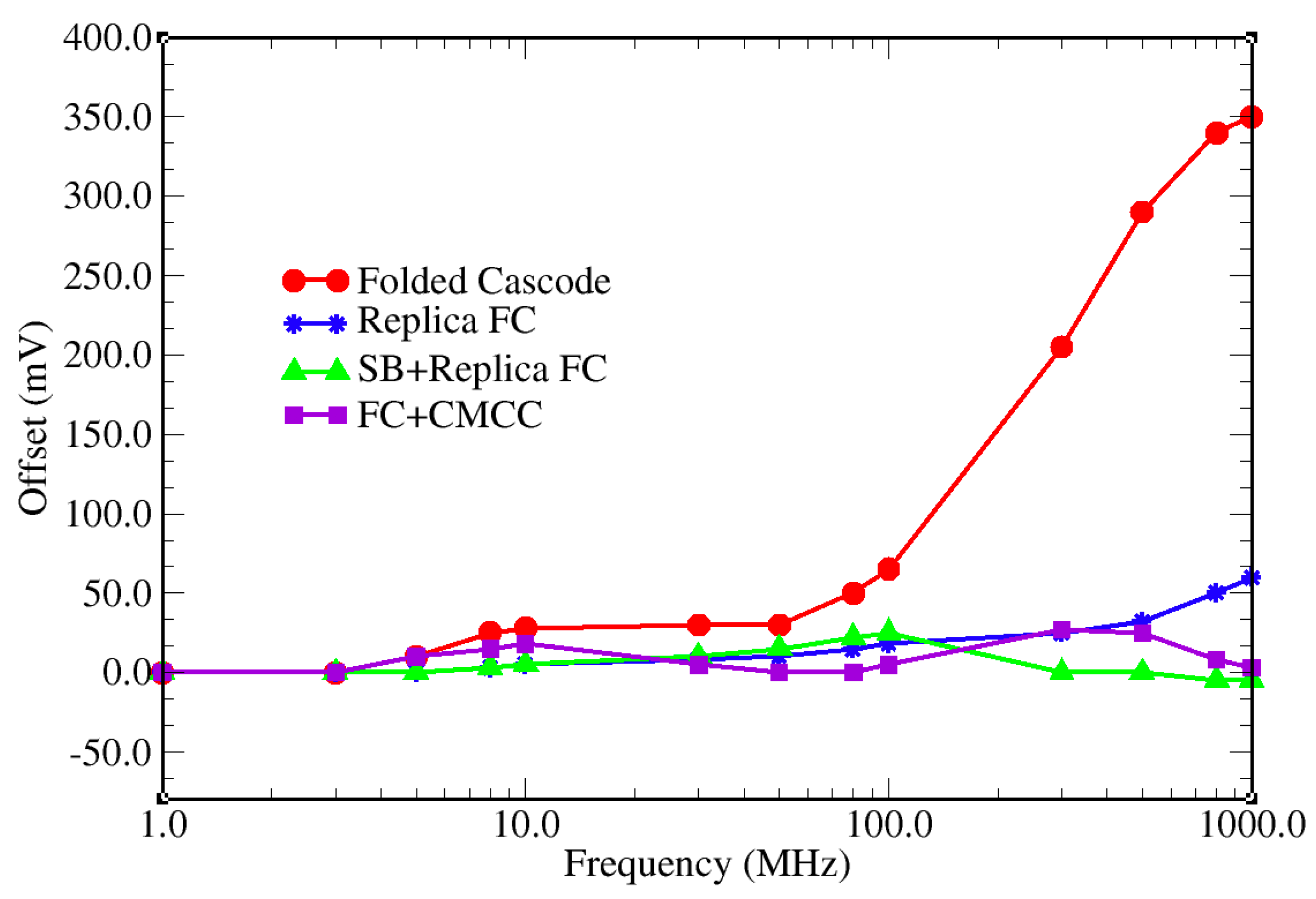
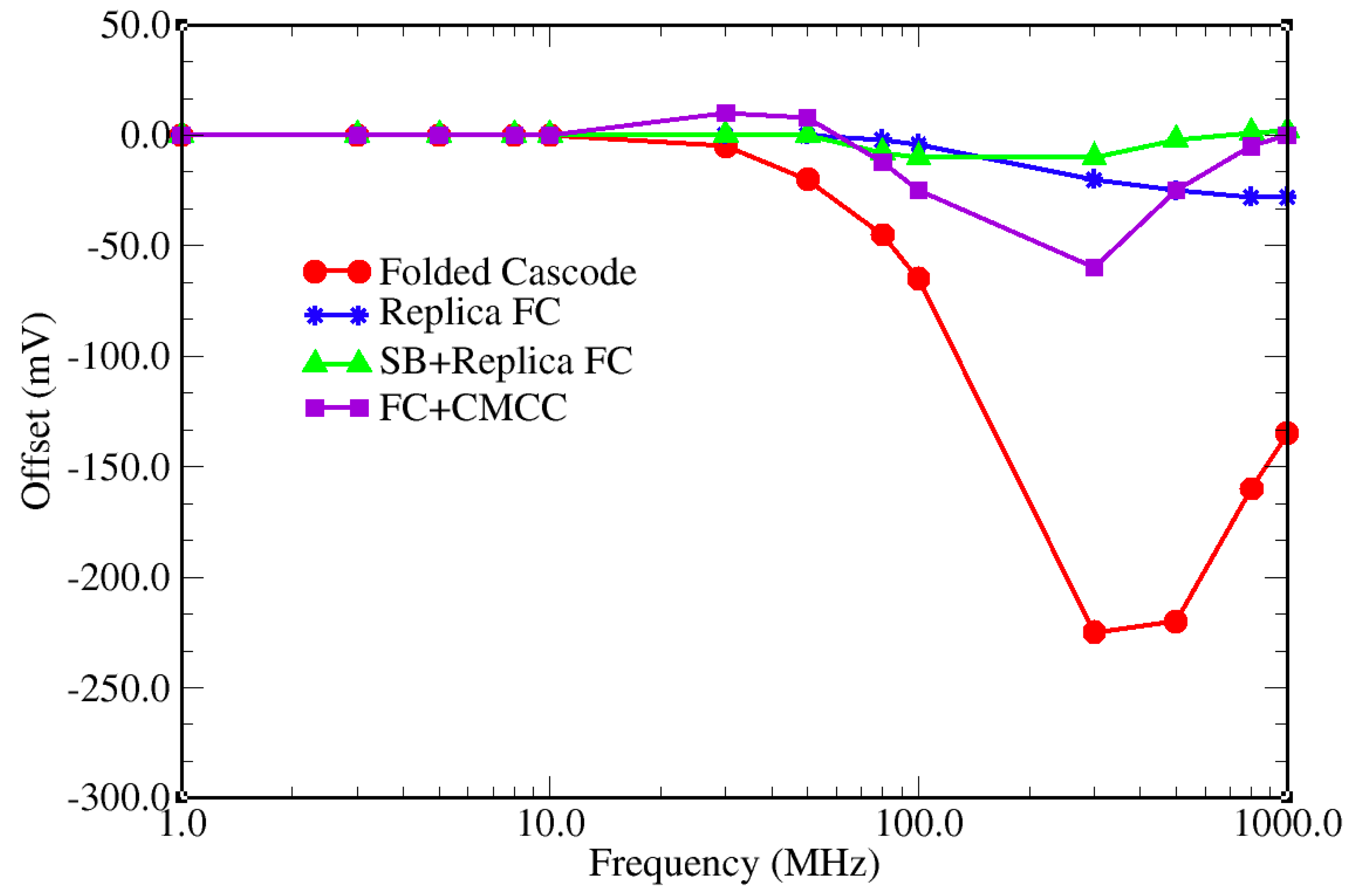
In the following step, the EMI susceptibility of these FC architectures is investigated and compared in the comprehensive EMI scenario, including also the interferences coupled from the ground plane of the PCB. First, the EMI are directly injected into the non-inverting input pin, and the offset of the output voltage induced by the interferences in all of the FC topologies are compared: the peak-to-peak amplitude of the interfering signal is half of the Vdd (1.65 V here). The results are plotted in Figure 11. As expected, the FC amplifier is susceptible at high frequencies, but the improved topologies exhibit a much smaller offset.
Then, the susceptibility with respect to EMI coupled to the output pin and to all of the pins is investigated and the results are shown in Figure 12 and Figure 13, respectively. From the figures, it is evident that the output pin is a critical injection point.

4. The Effect of the Voltage Buffer

If a voltage buffer is added to the second stage of the amplifiers, as shown in the left of Figure 14, the path of the interferences coupled to the output terminal changes because the impedance at that pin is changed. By considering the schematic shown in Figure 14, it is clear that the interferences coming from the ground plane run across a kind of high-pass filter, given by the parasitic capacitance and by the equivalent resistance R e q seen looking into the output node of the buffer stage. R e q is the low resistance 1/gm of the buffer decreased by the loop gain: at low medium frequency, 1/gm is still rather low. By adding the voltage buffer, the EMI coupling from the output pin becomes less efficient and the induced offset is strongly reduced to a few mV.
Moreover, we found that since the amplifiers are connected as voltage followers, the interference coupled to the output pin is fed back into the input. If the feedback between the output pin and the input pin could be interrupted somewhere, the interference coupled to the output pin would induce a much-reduced offset.

5. Conclusions

This paper compares different topologies in the comprehensive scenario of EMI pollution. These conclusions can be drawn: the architectures with higher immunity to the EMI directly injected into the input pin exhibit a much better immunity also with respect to the interference coupled from the ground plane. The output pin is a critical point of injection, and therefore, attention must be paid in the PCB design to reduce the coupling.

Author Contributions

All the authors contributed substantially to the paper. A.R., L.C., and Z.K.-V. supervised the work, provided the simulation tools, and wrote the paper; S.B. is a graduate of a five-year Laurea degree and designed the amplifiers and performed the experiments for his thesis.

Funding

This research received no external funding.

Conflicts of Interest

The authors declare no conflict of interest.

Abbreviations

The following abbreviations are used in this manuscript:
EMIElectromagnetic interference
CMOSComplementary metal oxide semiconductor
UMCUnited Microelectronics Corporation
GBWGain bandwidth
PCBPrinted circuit board
SBSource-buffered
FCFolded cascode
CMCCCommon mode cancellation circuit

References

  1. Redouté, J.-M.; Steyaert, M. EMC of Analog Integrated Circuits; Springer: Basel, Switzerland, 2010. [Google Scholar]
  2. Fiori, F. EMI-Induced Distortion of Baseband Signals in Current Feedback Instrumentation Amplifiers. IEEE Trans. Electromagn. Compat. 2018, 60, 605–612. [Google Scholar] [CrossRef]
  3. Ramdani, M.; Sicard, E.; Boyer, A.; Dhia, S.B.; Whalen, J.J.; Hubing, T.H.; Coenen, M.; Wada, O. The Electromagnetic Compatibility of Integrated Circuits-Past, Present and Future. IEEE Trans. Electromagn. Compat. 2009, 51, 78–100. [Google Scholar] [CrossRef]
  4. Lavarda, A.; Petruzzi, L.; Radez, N.; Deutschmann, B. On the Robustness of CMOS-Chopped Operational Amplifiers to Conducted Electromagnetic Interferences. IEEE Trans. Electromagn. Compat. 2018, 60, 478–486. [Google Scholar] [CrossRef]
  5. Masetti, G.; Graffi, S.; Golzio, D.; Kovács-Vajna, Z.M. Failures induced on Analog Integrated Circuits from Conveyed electromagnetic Interferences: A Review. Microelectron. Reliab. 1996, 36, 955–972. [Google Scholar] [CrossRef]
  6. Dhia, S.B.; Ramdani, M.; Sicard, E. Electromagnetic Compatibility of Integrated Circuits; Springer: Basel, Switzerland, 2006. [Google Scholar]
  7. Yu, J.; Amer, A.; Sanchez-Sinencio, E. Electromagnetic Interference Resisting Operational Amplifier. IEEE Trans. Circuits Syst. I Regul. Pap. 2014, 61, 1917–1927. [Google Scholar] [CrossRef]
  8. S, A.K.P.N.; Redouté, J.-M.; Baghini, M.S. A Generic EMI-Immune Technique for Differential Amplifiers With Single-Ended Output. IEEE Trans. Electromagn. Compat. 2018, 60, 958–964. [Google Scholar]
  9. Fiori, F. Design of an Operational Amplifier Input Stage Immune to EMI. IEEE Trans. Electromagn. Compat. 2007, 49, 834–839. [Google Scholar] [CrossRef]
  10. Richelli, A. EMI Susceptibility Issue in Analog Front-End for Sensor Applications. J. Sens. 2016. [Google Scholar] [CrossRef]
  11. Boyapati, S.; Redouté, J.-M.; Baghini, M.S. Modeling and Design of EMI Immune OpAmp’s in 0.18 μm CMOS Technology. IEEE Trans. Electromagn. Compat. 2016, 58, 1609–1616. [Google Scholar] [CrossRef]
  12. Chahine, I.; Kadi, M.; Gaboriaud, E.; Louis, A.; Mazari, B. Characterization and Modeling of the Susceptibility of integrated Circuits to Conducted Electromagnetic Disturbances Up to 1 GHz. IEEE Trans. Electromagn. Compat. 2008, 50, 285–293. [Google Scholar] [CrossRef]
  13. Ceperic, V.; Baric, A. Modeling of Electromagnetic Immunity of Integrated Circuits by Artificial Neural Networks. In Proceedings of the International Symposium on Electromagnetic Compatibility, Zurich, Switzerland, 12–16 January 2009. [Google Scholar]
  14. Gil, I.; Fernandez-Garcia, R. Characterization and modelling of EMI susceptibility in integrated circuits at high frequencies. In Proceedings of the International Symposium on Electromagnetic Compatibility, Rome, Italy, 17–21 September 2012. [Google Scholar]
  15. Fiori, F.; Crovetti, P.S. Prediction of high-power EMI effects in CMOS operational amplifiers. IEEE Trans. Electromagn. Compat. 2006, 48, 153–160. [Google Scholar] [CrossRef]
  16. Richelli, A.; Delaini, G.; Grassi, M.; Redouté, J.-M. Susceptibility of Operational Amplifiers to Conducted EMI Injected Through the Ground Plane into Their Output Terminal. IEEE Trans. Reliab. 2016, 65, 1369–1379. [Google Scholar] [CrossRef]
  17. Richelli, A.; Colalongo, L.; Toninelli, L.; Rusu, I.; Redouté, J.-M. Measurements of EMI susceptibility of precision voltage references. In Proceedings of the EMCCompo 2017, St. Petersburg, Russia, 4–8 July 2017. [Google Scholar]
  18. Boyapati, S.; Redouté, J.-M.; Baghini, M.S. A Robust CMOS Miller OpAmp with High EMI-Immunity. In Proceedings of the EMC Europe 2017, Angers, France, 4–7 September 2017. [Google Scholar]
  19. Boyapati, S.; Redouté, J.-M.; Baghini, M.S. A Highly EMI-Immune Folded Cascode OpAmp in 0.18 μm CMOS Technology. In Proceedings of the EMC Europe 2016, Wroclaw, Poland, 5–9 September 2016. [Google Scholar]
  20. Richelli, A.; Redouté, J.-M. Increasing the EMI immunity of CMOS operational amplifiers using an on-chip common-mode cancellation circuit. In Proceedings of the EMC Europe 2014, Gothenburg, Sweden, 1–4 September 2014. [Google Scholar]
  21. Grassi, M.; Redouté, J.-M.; Richelli, A. Increased EMI immunity in CMOS operational amplifiers using an integrated common-mode cancellation circuit. In Proceedings of the EMC Europe 2015, Dresden, Germany, 16–22 August 2015. [Google Scholar]
  22. Richelli, A.; Kennedy, S.; Redouté, J.-M. An EMI-Resistant Common-Mode Cancelation Differential Input Stage in UMC 180 nm CMOS. IEEE Trans. Electromagn. Compat. 2017, 59, 2049–2051. [Google Scholar] [CrossRef]
  23. Richelli, A.; Redouté, J.-M. A Methodological Approach to EMI Resistant Analog Integrated Circuit Design. IEEE EMC Mag. 2015, 4, 92–100. [Google Scholar]
  24. Redouté, J.-M.; Steyaert, M. EMI Resistant CMOS Differential Input Stages. IEEE Trans. Circuits Syst. I 2010, 57, 323–331. [Google Scholar] [CrossRef]
  25. Richelli, A.; Matig-a, G.; Redouté, J.-M. Design of a folded cascode opamp with increased immunity to conducted electromagnetic interference in 0.18 μm CMOS. Microelectron. Reliab. 2015, 55, 654–661. [Google Scholar] [CrossRef]
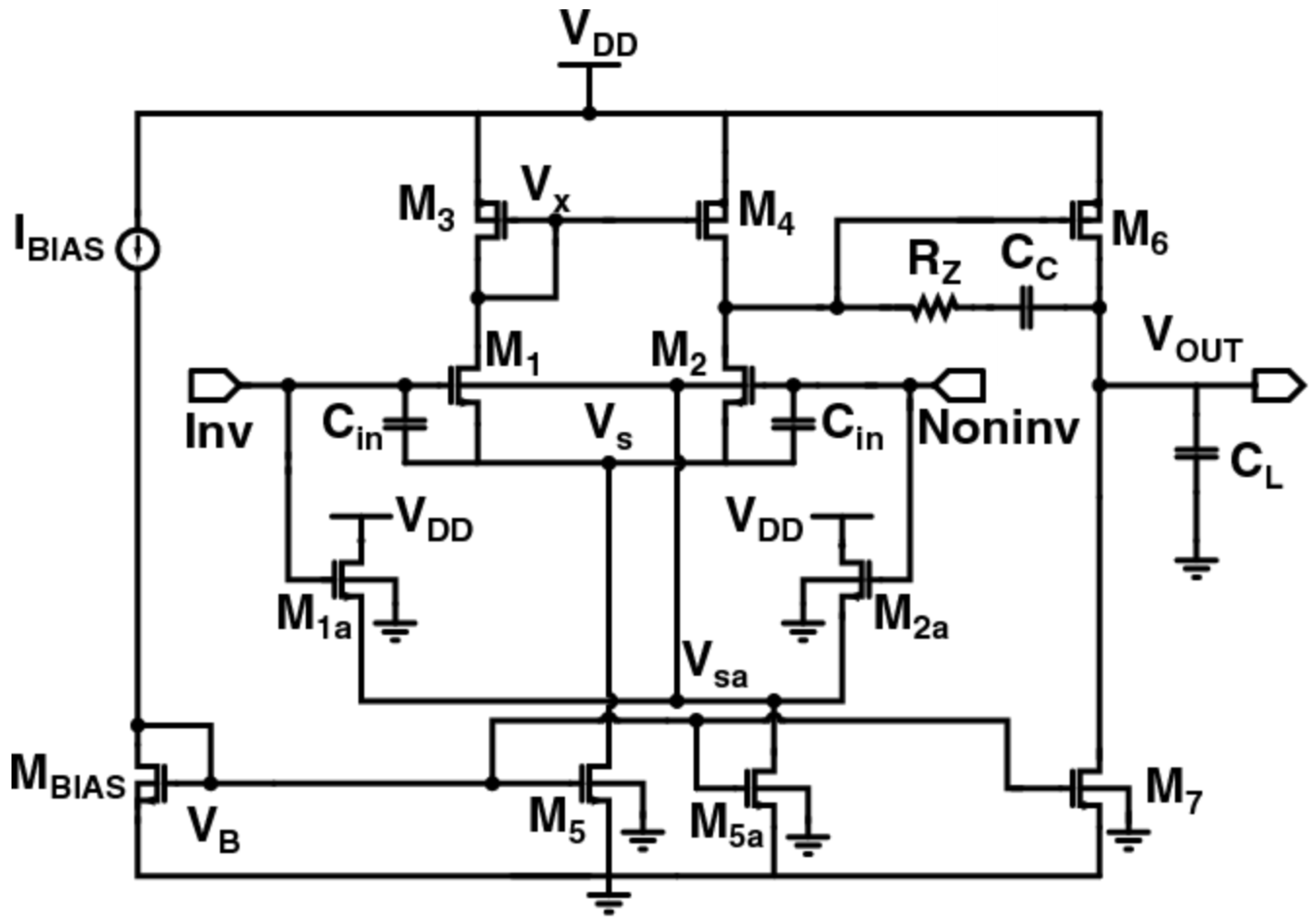
Figure 1. The source-buffered (SB) Miller amplifier proposed in [18].
Electronics 08 01181 g001
Figure 2. Simulations of the EMI effect: EMI directly injected into the non-inverting pin.
Electronics 08 01181 g002
Figure 3. Offset induced by 900 mVpp electromagnetic interference (EMI) in classic and SB Miller amplifiers.
Electronics 08 01181 g003
Figure 4. The classic input pair on the left and the source-buffered input pair on the right.
Electronics 08 01181 g004
Figure 5. Circuit for the simulations of the EMI effect: EMI coupled to the output pin.
Electronics 08 01181 g005
Figure 6. Circuit for the simulations of the EMI effect: EMI coupled to all of the pins.
Electronics 08 01181 g006
Figure 7. Offset induced by 900 mVpp EMI coupled from the ground plane of a classic and SB Miller amplifiers.
Electronics 08 01181 g007
Figure 8. Folded cascode with replica circuit to filter EMI.
Electronics 08 01181 g008
Figure 9. Source-buffered folded cascode amplifier with replica circuit and RC (resistor–capacitor) filter.
Electronics 08 01181 g009
Figure 10. Common-mode cancellation circuit.
Electronics 08 01181 g010
Figure 11. Offset induced by 1.65 Vpp EMI injected into the input pin of FC amplifiers.
Electronics 08 01181 g011
Figure 12. Offset induced by 1.65 Vpp EMI coupled to the output pin of FC amplifiers.
Electronics 08 01181 g012
Figure 13. Offset induced by 1.65 Vpp EMI coupled to all of the pins of FC amplifiers.
Electronics 08 01181 g013
Figure 14. Voltage buffer added in the amplifying chain.
Electronics 08 01181 g014
Table 1. AC and DC characteristics of the Miller amplifiers.
MillerSB Miller
Gain65.8 dB65.8 dB
f 3 d B 19.5 kHz19.7 kHz
GBW32.4 MHz32.3 MHz
Phase margin65.7°65.8°
Power consumption540 μ W620 μ W
Table 2. Transistors’ aspect ratios (W/L) [ μ m] in the Miller architectures.
MillerSB Miller
M1, M220/0.520/0.5
M3, M480/0.580/0.5
M5, M B I A S 60/160/1
M660/0.560/0.5
M720/0.520/0.5
M 1 a , M 2 a 10/0.5
M 5 a 50/0.5
Table 3. AC and DC characteristics of the folded cascode (FC) amplifiers.
FCReplicaSB ImprovedFC + CMCC
Gain60.9 dB61.8 dB61.2 dB66.6 dB
f 3 d B 21.6 kHz19.6 kHz19.9 kHz21.6 kHz
GBW23.9 MHz12.4 MHz11.3 MHz42.7 MHz
Phase margin85°84°84°60°
Power consumption1 mW1.3 mW1.5 mW1.2 mW
Table 4. Transistors’ aspect ratio (W/L) [ μ m] in the folded cascode architectures.
Replica FCSB + Replica FC
M1, M220/0.520/0.5
M 1 a , M 2 a 20/0.515/0.5
M3, M 3 a 6.05/0.56.05/0.5
M4, M542.5/0.642.5/0.6
M 4 a , M 5 a 42.5/0.642.5/0.6
M6, M72.5/0.342.5/0.34
M8, M94.75/0.344.75/0.34
M10, M114.75/0.344.75/0.34
M 1 s b , M 2 s b 20/0.5
M 3 s b 6.05/0.5