1. Introduction
The transimpedance amplifier (TIA) is defined as a sensitive and fast current measurement device which converts typically weak input current signal to the output voltage of considerable magnitude. Although the term TIA usually evokes an image of a resistive shunt-feedback (SFB) resistor approach [
1], this architecture has been the gold standard by providing a fair trade-off for the most important TIA parameters. Although, as is the trend for all microelectronics, the classical SFB TIA benefits from the continuous improvement in the technological processes, novel TIA topologies and circuit-level modifications have been constantly reported. Almost each newly reported work provides a novel or refined perspective on design with respect to the target trade-off between different performance measures while addressing some of the system’s or related technological constraints.
Although historically TIAs have been mostly developed for the front-ends of the optical receivers [
2], (e.g., the families of 2.5, 10, 40, ... GB/s), their usage is definitely not limited to optical-only applications, although those have been for longer the major driving force beyond the development towards both lower noise and higher speeds. Nevertheless, in recent decades advanced TIA designs are becoming increasingly popular for a variety of applications such as particle physics and radiation detectors, miniaturized magnetic resonance spectroscopy [
3], vision and biological sensors as well as inertial sensors such as Microelectromechanical Systems (MEMS) accelerometers and gyroscopes. As different applications usually have their own requirements for the main parameters of the TIA, the varying scenarios triggered an active search for improved and customized TIA designs. For example, high-speed optical communication circuits have pushed the bandwidth of TIAs in multiple GHz range, while the biological or inertial sensors benefit from the novel designs with lower power consumption, reduced chip area and minimized noise while operating at significantly lower frequencies. A different set of constraints must be considered while evaluating how to design the TIA for a particular application. The specifics of the domain often play a crucial role on the final decision on selecting a suitable topology for product implementation.
The context of a typical TIA application is presented in
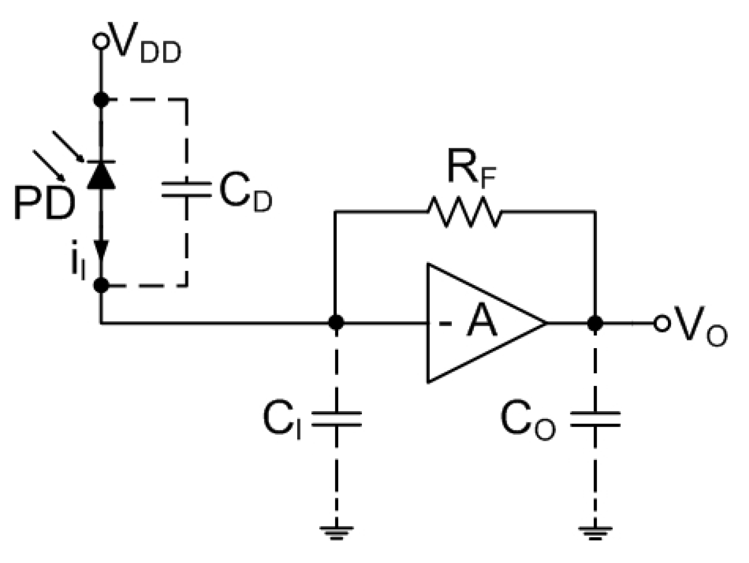
Figure 1. Here the TIA can be considered to be the first block (the other two are the filter and the main amplifier—MA) of a so-called linear channel for the input current processing. The linear channel is modeled as a complex frequency response which relates the amplitude and the phase of the output voltage to that of the input current. The modeling of the linear channel as a product of three responses is shown in
Figure 1. This is shown for depiction purposes and in practice the filter stage or the MA can be omitted or integrated into the TIA. As an input to the linear channel, a current
from the photodiode (PD) is shown with its noise current
. Clearly, any element providing a current input can be used in the given context. Here the noise characteristics of the linear channel are modeled as a single equivalent noise current generator
at the channel’s input (see
Figure 1). Although this noise current source is not white, it can be considered to be stationary and its amplitude distribution can be often well approximated as a Gaussian one. This is quite opposite for the statistics of a simple PD, which is typically approximated to have white, but non-stationary and non-Gaussian noise.
Obviously, the front-end TIA is the most critical component of the channel affecting both the noise-sensitivity and the speed of the overall system [
2]. At the output of the linear channel the voltage is provided which can be later used by either the signal processing or the decision circuits. Please note that here one assumes that the PD’s performance is not the limiting factor for the front-end and thus, the focus of the paper is put on the improvements of the TIA design. Still, one has to be aware that different detectors or current sensing elements may have varying primary noise mechanisms which need to be considered while performing the circuit-level simulations and when assessing the feasibility of the candidate TIA design for a very particular application. For example, although the shot noise is believed to be a major noise source for PIN type detectors, avalanche noise with the excess noise factor must be considered if an Avalanche Photodetector (APD) is utilized. Furthermore, it is also assumed that the PD is sufficiently linear so that the signal distortions are minimized.
Until recently, the higher performance TIAs were often implemented in GaAs, HEMT, HBT and SiGe BiCMOS technologies due to their speed, noise, bandwidth and gain advantages [
4]. Here the decision has been made to employ a conventional low-cost deep-submicron CMOS due to its low-cost and high integration characteristics—the so-called “holy grail” for system-on-chip (SoC) solutions [
4]. In fact, the submicrometer CMOS technologies have provided sufficient performance for radio-frequency applications in 1–2 GHz since back in 2000 and, therefore, the performance of modern CMOS processes is more than sufficient for the intended 1 GHz Optical Time-Domain Reflectometry (OTDR) application. Although a discussion on performance of CMOS against III-V technologies probably deserves its own paper similar to that on CMOS for RF power amplifiers [
5], some brief discussion may still benefit this review work. Definitely, for the high-volume production, the costs of the standard CMOS are relatively low and are continuously decreasing over the past several decades. There is also a large production capacity available at the foundries and one does not need to own a custom line to keep up with the trends in the market [
5]. Furthermore, from the system perspective the non-TIA components such as the processing logic etc. can be easily integrated with the TIA if desired while achieving almost any level of integration [
6]. Of course, when having the data processing and the interface chips with different technologies, the packaging costs may increase while the overall system performance may decrease due to interconnecting bond-wires and pads [
7]. Here the availability of millions of cheap transistors allows easy addition of the performance-enhancing functionality including complex bias circuits and advanced Electrostatic Discharge (ESD) design procedures—something which may be not easily available for III-V technologies. Although this work concentrates on CMOS TIA design, one shall not eliminate III-V technologies from the consideration. These technologies are continuously becoming feature-rich and with the addition of field-effect transistors to most of HBT processes designers now have higher flexibility in implementing circuits for more advanced and specific applications [
5].
For cost-saving purposes CMOS technology presents an excellent candidate to design a truly low-cost and low-power TIA; however there are significant technical challenges which make the development path more than non-trivial. These technical challenges are mainly related to the contradicting requirements of a typical TIA such as high-gain, large bandwidth and, at the same time, low input noise [
8]. Here increasing the gain usually increases chances of instability, while the requirement for lower noise performance often translates into higher power consumption. Furthermore, typical CMOS technological challenges have to be also addressed such as severe parasitic capacitances [
9], supply voltage limitations, relatively low transimpedance and noise performance as well the inherent bandwidth limitations caused by large PD capacitance, where the latter is often responsible for the dominant pole in TIA and leads to the corresponding bandwidth constraints [
7,
10,
11]. Finally, even though the reduction of the channel width does not shrink the size of analog circuits in the same way it does for digital ICs [
12], such scaling may significantly increase the costs. Therefore, the specific technology shall be carefully selected as a trade-off for both the performance and the costs.
As a relatively large number of the design solutions for CMOS TIAs have been reported in the literature with each approach targeting an application-specific trade-off of the main circuit parameters, a basis for the performance comparison needs to be selected as a unified and a clear measure for relative positioning of the numerous designs reported in recent years. For example, while optical communications do not consider the linearity of the TIA as a crucial performance measure, this may become important for non-optical applications such as magnetic resonance imaging [
3]. Even though a tabulated report on the major circuit characteristics is almost always needed for the completeness of the discussion or to convince the reader that a proposed design is definitely better than all those published before, the selection of the competitors is usually rather limited with up to 8 or 10 alternative solutions for comparison. Moreover, a tabulated specification of the main TIA parameters often results in a mixed or an unclear impression on the superiority of the proposed scheme based on one or a few key parameters from the set. Unfortunately, some of the parameters important for OTDR applications may not be reported in the most cited works on CMOS TIA for optical communications as these parameters may have a lower priority when compared to the gain and bandwidth for mainstream applications such as receivers for optical communication systems [
13]. As with some of the previous works, we try to address a problem of a unified performance metric by introducing a so-called Figure of Merit (FOM), which can be used, at least till some extent, as a single criterion for the TIA’s performance assessment. Clearly, the main requirement for this performance measure is that it should provide a fair balance for the most common TIA measures such as the amplifier’s bandwidth, transimpedance gain, noise, the power consumption, etc. Although several approaches have been suggested in the literature [
7,
9,
11], they have their own limitations. For example, some works [
7,
9] do not include the PD’s capacitance and the noise level with the latter often considered to be a critically important design criterion for higher performance TIAs. On the other hand, the complex FOM as suggested in other works may include a penalty due to the number inductances used in the design. However, counting inductances results in implicitly penalizing the area of the design similarly to FOM proposed in [
7] which we would like to avoid due to several reasons. First, not all works explicitly report the design area or make a clear separation between the TIA front-end and the rest of the circuit. Secondly, the area may be not a good criterion as not all research works try to minimize the area of the final circuit as often the major objective is to improve the other circuit parameters.
Although the pursuit for a higher TIA performance has a much broader scope than the original application of the circuits for optical communications, we believe that a fair comparison and even an analysis of the unified performance metrics for TIA shall, nevertheless, consider an intended application domain of the circuits. The provided review is done within the context of developing a custom TIA for a front-end of higher performance, but nevertheless, lower-cost OTDR. Untill recent, the TIAs as used in commercial OTDR instruments were often implemented using discrete components [
14]. Thus, due to their large parasitic capacitances, the bandwidth of typical circuits was limited to between 50 and 70 MHz significantly limiting the performance of available instruments [
12]. Furthermore, the discrete solutions are more vulnerable to noise leading to significant limitations when trying to achieve higher dynamic range and signal-to-noise ratio [
14]. A TIA implemented as a complete integrated circuit would result in lower parasitic capacitances and, due to significantly increased bandwidth, would lead to a dramatic decrease in the dead zone when compared to existing discrete solutions. For the OTDR instrument, similarly to other applications, the TIA appears to be the most critical part of the optical receiver (see the classical discussion in [
2]) and its performance has a dramatic impact on the overall characteristics of the instrument [
15,
16]. Obviously, the specifics of OTDR instrumentation may mandate significant circuit innovations when compared to typical TIAs designed for optical communication networks. We believe that a CMOS TIA for a higher performance albeit low-cost OTDR instrument may heavily rely on circuit design techniques to overcome the technology shortcomings. The presented work tries to provide a systematic overview of the design methodologies and a fair comparison of the reported CMOS TIAs topologies as well as circuit-level solutions in the context of the envisioned OTDR application. Within the review, we will try to discuss and point out the issues which may be relevant for the OTDR applications according to the summary of the requirements and specifics of the application domain as presented in
Section 2 below.
The rest of the paper is organized as follows:
Section 2 presents a concise overview of the working principles behind OTDR, while
Section 3 provides a general discussion on several classical TIA designs.
Section 4 presents a detailed discussion on a set of recently reported CMOS TIAs with an in-depth discussion on the trade-off of each approach. Based on these findings,
Section 5 provides a discussion on the suitability of some of the reported topologies for an intended OTDR application with
Section 6 summarizing the contribution of the paper and providing the outlook for the future TIA implementation.
2. Optical Time-Domain Reflectometry
The OTDR is a well-established tool for investigating the attenuation characteristics of optical fibers [
17]. Usually, OTDR is employed to characterize the faults, loss and damage along the optical fiber link, where the precise location of the faults can be resolved along with the nature of the problem. OTDR can be also used to evaluate the fluctuations of the fiber’s parameters and is extremely useful for the case of optical transmission lines composed of several optical fiber cables. Moreover, OTDR is also often used for estimating the capacity and real-time performance of Passive Optical Networks (PON) [
18]. The methods of OTDR employ the measurements of the time-delayed version of the Rayleigh Backscattering (RBS) signal or the Fresnel reflections from the incident optical power (e.g., injected optical pulse) along the fiber to provide a complete figure on the fiber’s loss characteristics as a function of its length. The method allows the splice and the connector losses to be evaluated and delivers an estimate for the location of any faults in the optical link under test. During the OTDR operation, relatively narrow optical pulses are injected into the splitter and then propagate down the fiber. As the signal comes across the discontinuities along the fiber, a fraction of the light is rejected and routed back through the splitter to the receiver. Based on the timing and the amplitude of the rejected pulse, the location and type of the fault in the fiber can be determined. Moreover, even in the fiber without a fault, some rejections do occur due to Rayleigh scattering which is caused by variations in the density or composition of the fiber material. This scattering mechanism is a dominant loss mechanism in the state-of-the-art fibers for typical operating wavelengths.
In OTDR applications the relationship between the frequencies of the incident and scattered light determine the effect of the light scattering in the fiber. In the case of elastic scattering, the frequency of the incident and scattered photons are equal. RBS is an example of such a mechanism, where the scattering occurs due to the linear transfer of the energy between the modes. RBS is caused by the density and the structure of the fiber material [
19]. By contrast, in inelastic scattering the frequencies of the incident and scattered photons are not equal. Spontaneous Raman Scattering (SRS) is a good example of this inelastic process. Here the incident optical signal stimulates the molecular vibration of the silica material and final energy of Raman Stokes scattering is higher than that of the initial state, while the final energy state of anti-Stokes Raman scattering is lower than that of the initial energy state. The frequency of the scattered photons shifts to a particular value which is equal to the characteristic vibration frequencies of the molecules determined by the Raman spectrum of the fiber material. Please note that in Raman OTDR one must ensure the incident power to be larger than the threshold value for SRS to take place.
When a peak power of the injected optical pulse is limited, there is a trade-off between the width of the pulse and the spatial resolution [
17], where a broad optical pulse increases the dynamic range by sacrificing the spatial resolution of the instrument. The effect can be mitigated by so-called correlation OTDR, where a pseudo-random bit sequence is used to modulate the optical pulse and the correlation between the backscattered light and the delayed bit sequence is obtained by the cross-correlator.
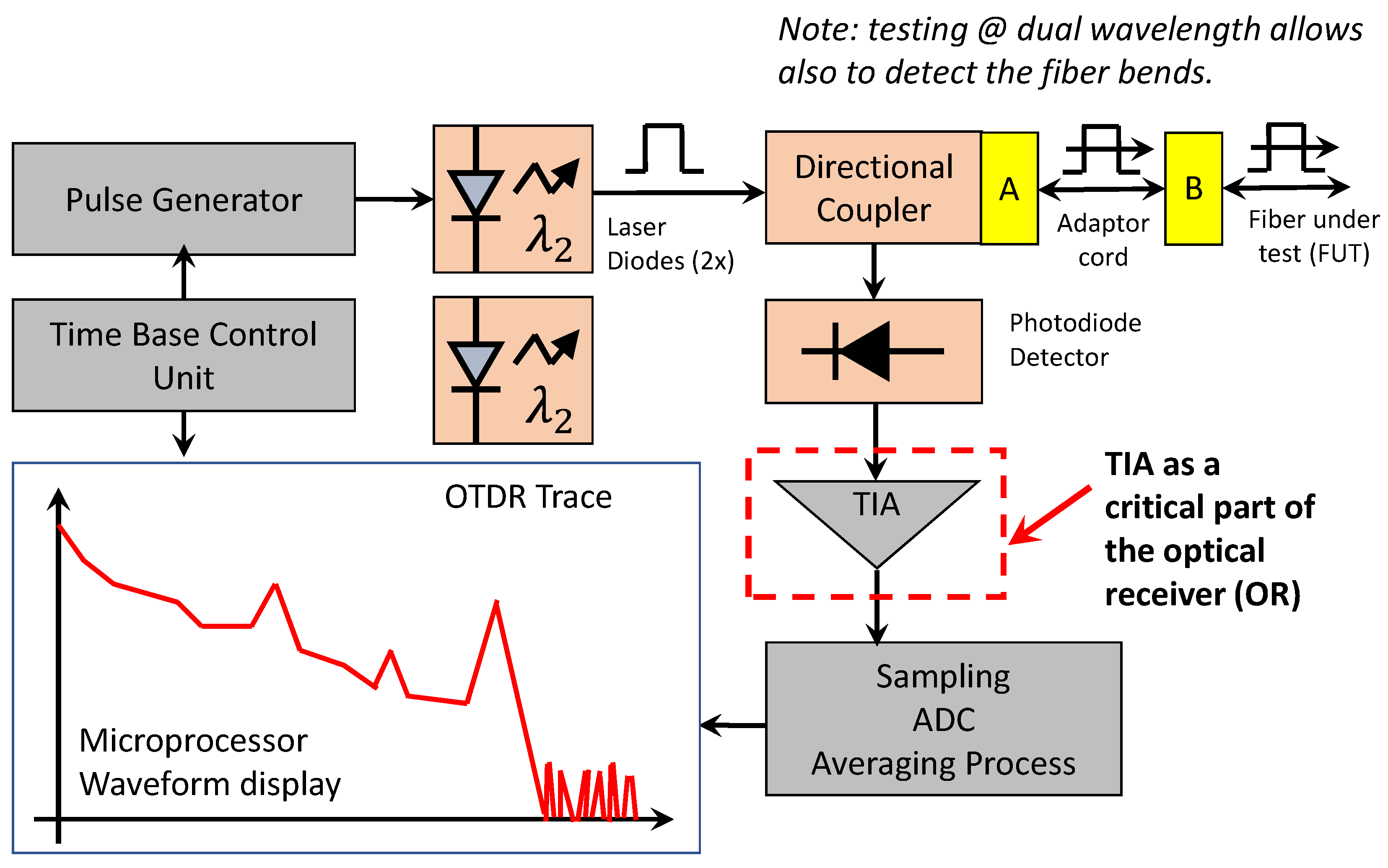
A typical OTDR instrument may contain several parts or modules which provide the required functions. These modules may include the waveform generator (one or more laser diodes), a detector, a signal processing unit and a display. The instrument should also provide capability to connect to the fiber under test using, for example, a directional coupler. The block functions of a typical OTDR instrument are shown in
Figure 2.
The key characteristics of the technique are the attenuation dead zone (ADZ) and the dynamic range (DR), where both depend on the laser’s pulse width and the bandwidth, and where the DR also depends on the laser’s power and receiver’s SNR. An ideal OTDR shall have a zero ADZ and infinite DR. However, such an ideal configuration can be only achieved for the case of a noiseless optical receiver with infinite bandwidth and delta-function type laser pulses [
12]. In practice, the laser power is limited to approximately 1W by the nonlinear Kerr effect and the pulse width must be increased to deliver more energy into the fiber [
12].
Several parameters of the OTDR usually have an impact on the performance of the instruments. First, the width of the injected optical pulse controls the amount of light provided to the fiber. A short pulse width enables high resolution and short dead zones, but results in a small dynamic range of the instrument. On the other hand, a longer pulse width enables high dynamic range but leads to reduced resolution and larger dead zones. Furthermore, the acquisition time is defined as the time during which the OTDR instrument acquires and averages the data points. By increasing the acquisition time one can improve the dynamic range without affecting the resolution and the dead zones. Finally, the time-domain measurements as obtained by the OTDR are mapped to distance along the fiber using the available index of refraction. The obtained characteristic (called the
trace of OTDR) provides a visual interpretation of the measurements and can be effectively mapped to the length measurements of the fiber (
Figure 2).
The availability of high-speed and high-density Application-Specific Integrated Circuit (ASIC) technology has made it possible to integrate the functions required to create the OTDR measurements on a single chip [
14] and even use the OTDR capability directly in the optical transceiver modules [
20]. Several interesting works have been recently reported which have adressed a problem of minimizing complete OTDR modules via a higher integration level. For example, a single chip integration OTDR ASIC developed by Ultra Communications Inc. for higher resolution OTDR applications was recently announced [
20]. The system provides the necessary clocking, timing/pattern generation (arbitrary 20-bit pattern), receiving and sampling functions needed to implement an OTDR within a compact transceiver module and physical layer components while being only 4.0 mm × 1.655 mm. The programmable timing circuits can operate up to 10 GHz with current-mode output logic output and a four-channel receiver/sampling circuit. The presented ASIC can generate pulse widths of 100 ps and sample at 100 ps resolution, which is approximately equal to the round-trip time for an optical pulse to travel 1 cm in fiber. Moreover, within the architecture, the pulse width can be easily adjusted by setting a different bit pattern while enabling both flexible and low-cost implementation of OTDR within physical layer components. According to the authors, both the offset and the gain of TIA and associated post-amplifiers could be tuned appropriately for detecting small and large signals.
A System-on-Chip (SoC) solution for OTDR had been also demonstrated in [
18]. The developed circuit could be configured into several modes including high-performance mode (external modulator, expensive off-chip laser and PD) as well as low-cost mode (low power/gain with inexpensive laser and PD). The developed circuit achieved a maximum detectable fiber length of 25 km with the spatial resolution of 2.5 m, 4 m and 10 m depending on the configuration. When compared to the current discrete solutions (year 2016) on the market, the integrated system was expected to reduce the cost by factor 100×, area by factor 5× and power consumption by 4×. As the received signals due to Rayleigh backscattering were below the noise level of the system, only the measurements of Fresnel reflections could have been demonstrated.
Recently, yet another ASIC implementation of the OTDR module had been demonstrated in [
14]. The OTDR ASIC was implemented using 350 nm CMOS process and occupied the area of 5 mm by 4 mm while operating from 3.3 V power supply.
Unfortunately, almost no TIA designs have been reported specifically for OTDR applications. Although no details on TIA architecture or its performance characterization have been reported in the original publication of [
20], the detection scheme as proposed by the authors was designed to measure only the reflective events in the optical pathways and not the RBS, which is, probably, an indicator that no special requirements for the TIA performance have been set and a classical resistive SFB TIA may have been used. The authors in [
18] employed a two-stage TIA with common-mode feedback and corresponding amplification stages of 20 dB and 10 dB respectively. The TIA is followed by a second-order low-pass filter with biquad architecture and 20–40 dB tunable gain (step size of 10 dB). Furthermore, an inverse Thomas-Tow biquad technique and DC offset cancelation are employed for low-noise and offset compensation. Finally, the authors have placed a programmable gain amplifier between the filter and the output buffer to provide a final amplification for an output scale of 30 dB with a 1 dB step.
The newest work [
14] employed a classical resistive feedback TIA, where additionally a feedback capacitance was added in parallel with the feedback resistor. While the transimpedance gain of the TIA was mainly determined by the feedback resistor
, the feedback capacitance
helps to improve the stability of the TIA. The resistor mux was designed for adjustable transimpedance gain. The core voltage amplifier was designed as a 2-stage OP-Amp due to simultaneous requirements on high bandwidth and wide output swing. The authors also implemented a sample and hold amplifier to decouple the TIA from a Successive Approximation Register (SAR) Analog-to-Digital Converter (ADC) as the ADC may load down the TIA affecting the overall performance of the system.
A unique work on addressing specifically TIA design for OTDR is [
12], where a variable gain fully differential SFB TIA was proposed. The variable gain was implemented with feedback resistors connected in series using the single-pole double throw (SPDT) switches to reduce input parasitic capacitances with five resistor pairs used to achieve the desired range of the gains. A self-biased topology was chosen, and a start-up circuit was added to avoid an unwanted bias state. Unfortunately, the author does not go beyond a classical SFB TIA and exact noise figures are not provided to facilitate a juxtaposition to the other reported TIAs. Therefore, the comparison of the reported CMOS TIA designs as presented in this work is done without an explicit application domain constraint and the TIAs are selected from similar (mainly optical) applications.
The sensitivity of an optical receiver can be limited by various noise sources, both in the detector and in the following amplifier. Originally, two options may have been considered for developing a low-noise input stage for OTDR either by using a high-impedance or a TIA. Nevertheless, the latter type is preferred for amplification of the backscattered signals due to its superior dynamic range. However, the noise performance of both approaches is similar (the feedback resistor of TIA becomes the load resistor in high-impedance approach). As the TIA-based strategy may be considered to be a well-established technique for the design of high-performance optical receivers, it had been selected for OTDR application.
To evaluate properly the suitability of the reported TIA topologies for the intended application, a preliminary specification for the CMOS TIA shown in
Table 1. The bandwidth of the TIA must be adequate to reproduce the shortest pulse length and, thus, the degradation of the range resolution in a final OTDR system can be avoided. Out of these preliminary requirements, one should point out two which make the design rather non-trivial: the relatively low noise requirement (<5 pA/
) for the given bandwidth and the flatness of the frequency response (0.1 dB). These two requirements eliminate most of the standard high-speed architectures and could need special handling including revision of an approach which is typically used for OTDR application—i.e., classical resistive shunt-feedback TIA. The requirement on the flatness of the frequency response may also challenge widely adopted techniques of inductive broad-banding or those might be applied with greater care. As the work addresses the design of a single-channel TIA, no special consideration for crosstalk performance is, probably, required, while particular treatment expected to ensure the specification conformance for a broader range of transimpedance gains. Finally, no constraints are given in terms of the chip area, although, naturally, one should seek for area minimization when targeting commercial low-cost applications. Please note that the design of TIA as an integrated circuit leads to an increased flexibility in circuit tuning and noise optimization via the device geometry adjustment, when compared to the design with discrete components [
21]. Here special design optimization techniques can be used to find optimal values for the geometry of separate elements. This becomes an important feature which is simply not possible when designing the TIA from discrete components.
Please note that the TIA shall be designed to operate with the as large as 500 fF and input capacitance (ESD, etc.) of additional 500 fF. The need to support such large capacitances arises due to PD being external to the chip with correspondingly large bondpad capacitances. A lower input capacitance would permit a higher input impedance and allow smaller devices to be used in TIA resulting in substantial power savings, while retaining the same bandwidth and improved sensitivity or increased bandwidth with the same sensitivity.
A special challenge of the proposed CMOS TIA is the requirement of the variable gain. Although the original work on OTDR-specific TIA [
12] reported a variable gain SFB TIA, a practical implementation may be non-trivial if the rest of the constraints need to be fulfilled with a single global TIA structure. Furthermore, depending on the topology finally selected for the TIA, it may be non-trivial to implement a variable gain while changing only one parameter of the circuit (i.e., such as implemented with feedback resistor in [
12] or [
14]) and advanced design methodologies may be needed. Please note that the specification does not have an explicit requirement for the phase linearity and the group delay variation for the TIA as well as no constraints on the die size are presented.
The specification, as shown above, corresponds to high-resolution integrated OTDR based on RBS and Fresnel reflections. On the other hand, the methods of OTDR are often used in combination with SRS to implement distributed temperature sensing [
19] as the anti-Stokes components of SRS are strongly sensitive to temperature. This nonlinear effect allows the optical fiber to act as a distributed sensor which can replace many point sensors [
22] with the detector placed at the beginning of the fiber cable. The technique is capable of providing many sensing points over a wide area and has been successfully used in spectroscopy and different monitoring applications. Please note that the optical fiber acts as a combination of the transmission medium and the sensor, where the monitoring of backscattered optical Stokes and anti-Stokes components takes place. An interesting idea on combining both RSB and SRS was proposed in [
23] to support an integrated background correction function as the change in background transmission properties of the fibers (e.g., due to ageing effects) can be distinguished from pure thermal effects.
Unfortunately, conversely from classical OTDR, where recently several ASIC have been reported (see [
14,
18]) and special OTDR-specific TIAs have been considered [
12], no similar works are known to the authors for Raman OTDR applications. Typically, for Raman OTDR applications a laboratory equipment with APD and data acquisition cards are employed (see [
19,
24]). As no details on the built-in APD or external TIA are provided, very little information can be extracted on Raman OTDR requirements for TIAs. The major difference is that as high spatial resolution for distributed temperature sensing is typically not required, the TIA for Raman OTDR application may need significantly lower bandwidth (on the order of several to tens of MHz) when compared to the specification in
Table 1. The work [
24] reported on the amplifier bandwidth of 50 MHz, while a TIA with only 3 MHz bandwidth was employed in [
25].
4. Reported Results and Performance Evaluation
As we have discussed in the introduction, the CMOS TIA performance comparison may benefit from adopting a unified performance measure in the form of FOM. For the presented overview we suggest adopting the following FOM:
where
is the bandwidth in GHz,
is the transimpedance gain in
,
is the combined PD and parasitic capacitance,
P is the power in mW and the
is the input noise current density. Please note that differently from the work of Atef [
6], an input current noise density is used instead of an equivalent input noise and this is exactly the reason a square-root of the bandwidth is taken in the numerator of the expression above. Alternatively, the FOM metric of Atef [
39] can be also used:
It is interesting to notice that both metrics show the best results for the same design and in general may be considered to be equivalent. If the works do not specify the value of
, a default value of 0.5 pF is used for the FOM calculations. We consider this to be a reasonable assumption as the values in practice are between 0.2 pF and 0.6 pF for external photodiodes. For most of the works it may be unclear whether the reported
is a true PD capacitance, or a combined value including the parasitic capacitance such as the one due to ESD protection diode and pad (The parasitics due to ESD protection and pad may be as high as 0.5 pF as reported in [
15]). Simpler FOM metrics have been also used historically. For example, in their series of works on PIP TIA Jun-De Jin et al. [
9] have used the gain-bandwidth product per DC power as some FOM approximation:
Even though this FOM may work fairly well for benchmarking the TIA’s for high-speed optical communications (e.g., 40-Gb/s addressed in [
9]), the metric does not penalize the designs with large noises and does not consider the value
which may have a detrimental effect on the achievable bandwidth of the amplifier. Usage of such FOM may benefit simpler and faster TIAs with significant noise and can unjustly penalize the topologies targeting low-noise applications.
Clearly, if a particular design does not report on some of the other critical performance measures such as power consumption, no FOM value could be calculated. In this case, the design will be still described in the summary parameter table below and only FOM numbers may be missing. As is clear from the expression above, we have also chosen the strategy not to penalize, explicitly or implicitly (e.g., via counting the inductances) the area of the proposed design. There are several reasons for this decision. First, numerous works do not report the total chip area especially is the results are reported for simulation only and no post-layout simulation had been performed. Furthermore, some works report the area only for the front-end TIA while considering the rest of the auxiliary circuits of minor importance, while still the others include the total design area with the buffer. Thus, the inclusion of the area for this design may significantly bias the ranking. Finally, as a lot of designs have been reported by academic research groups, it becomes unclear on how much effort has been really invested on minimizing the final chip area especially when this is often not the key requirement in research projects.
The summary of the performance of the selected TIA as reported in the original works is shown in
Table 2. When a total input noise current is specified by the authors, the noise density is calculated using the provided bandwidth values. The FOM is calculated using the first approach described above. Please note that in some cases the authors either do not specify the value of the
or specify together with the rest of the input parasitics. Moreover, in some cases, the power consumption cannot be clearly separated between the TIA front-end and the rest of the circuit. Bearing all this in mind the FOM shall be only considered to be a rough indicator and as an approximation of ever evading unified performance metric. The works are sorted in the order of publication to avoid biasing in terms of one performance indicator.
The discussion shall be, probably, started from the series of works of Toumazou and Park dating back to 90s. In their first works [
46,
47] (not shown in
Table 2) the authors developed a CG TIA with an additional feedback resistor from the output to the drain of the input-stage transistor which gives an additional tuning knob to control the dominant pole of this feedback amplifier. In their later work [
34] the authors addressed a problem of TIA’s bandwidth and noise performance constraints by using an RGC input stage with the subsequent voltage follower and again the feedback resistor to the drain of
. The authors demonstrated the RGC TIA to outperform the equivalent CG solution both in terms of the power consumption, gain and noise. Unfortunately, the original work [
34] does not specify the value of the input parasitic capacitance for which the simulation was performed and for the FOM calculation a default value of 0.32 pF was assumed from the previous work of the authors [
47]. Furthermore, relatively large overall power consumption along with the moderate gain did not allow this design to achieve high FOM values.
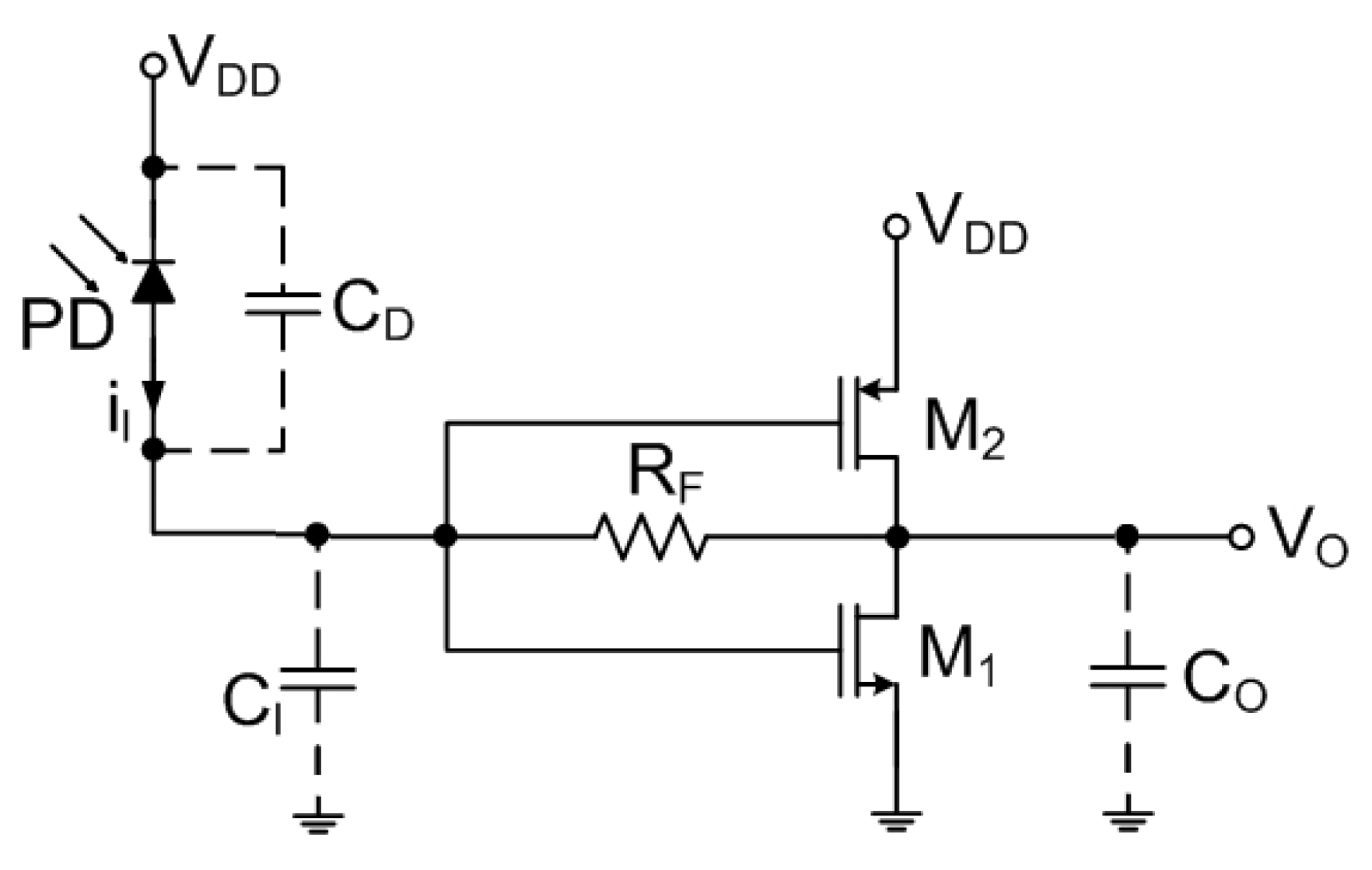
Relatively simple push-pull single stage [
8], three [
28] or five cascaded stages [
29] TIA have been also proposed. In all the cases either NMOS or PMOS devices biased in the triode regions were employed to optimize the noise when replacing a default resistor in the feedback path. The [
8] also suggested to use an additional inductor in the feedback path to extend the bandwidth, while the work [
29] suggested to use a series inductive peaking before the last inverter stages. Although the nominal performance of these simple designs seems to be good (especially [
8]), the simulation results are only presented, and no measurements are provided to confirm the final performance. Furthermore, the inductances introduced significant peaking in the passband which may be not acceptable for OTDR applications and the work does not detail on the PD capacitance used for simulation [
8] or even no power consumption and PD capacitance given in [
29].
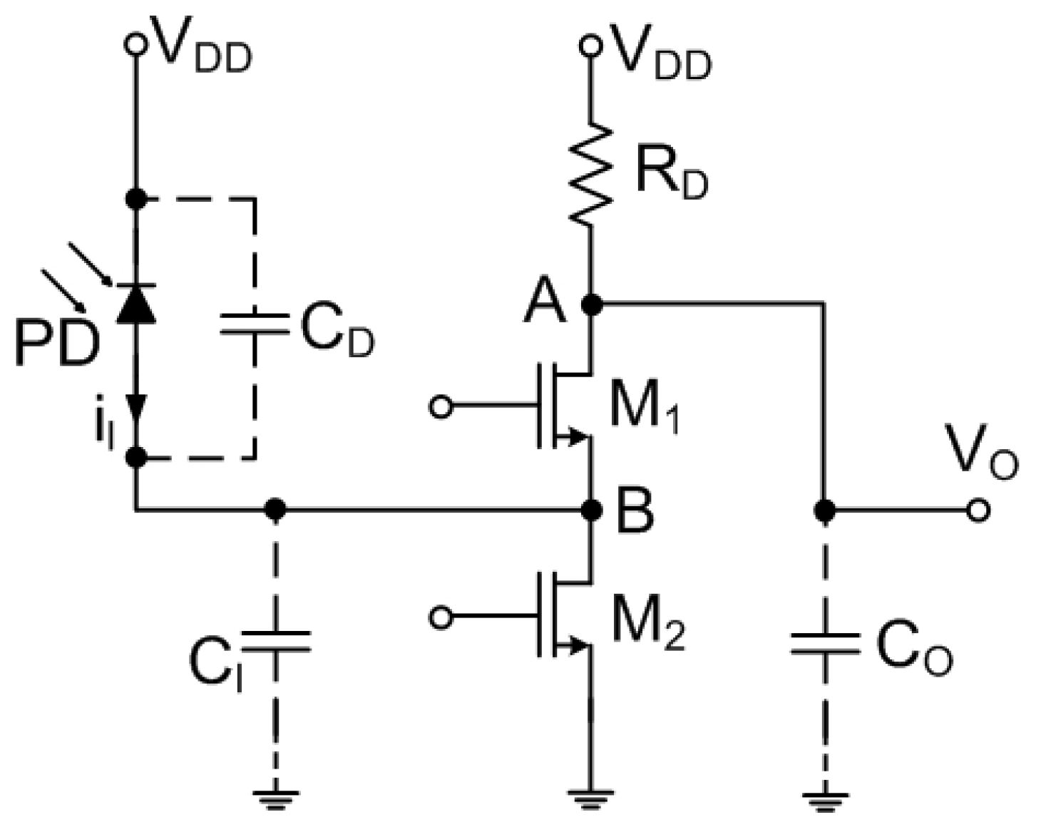
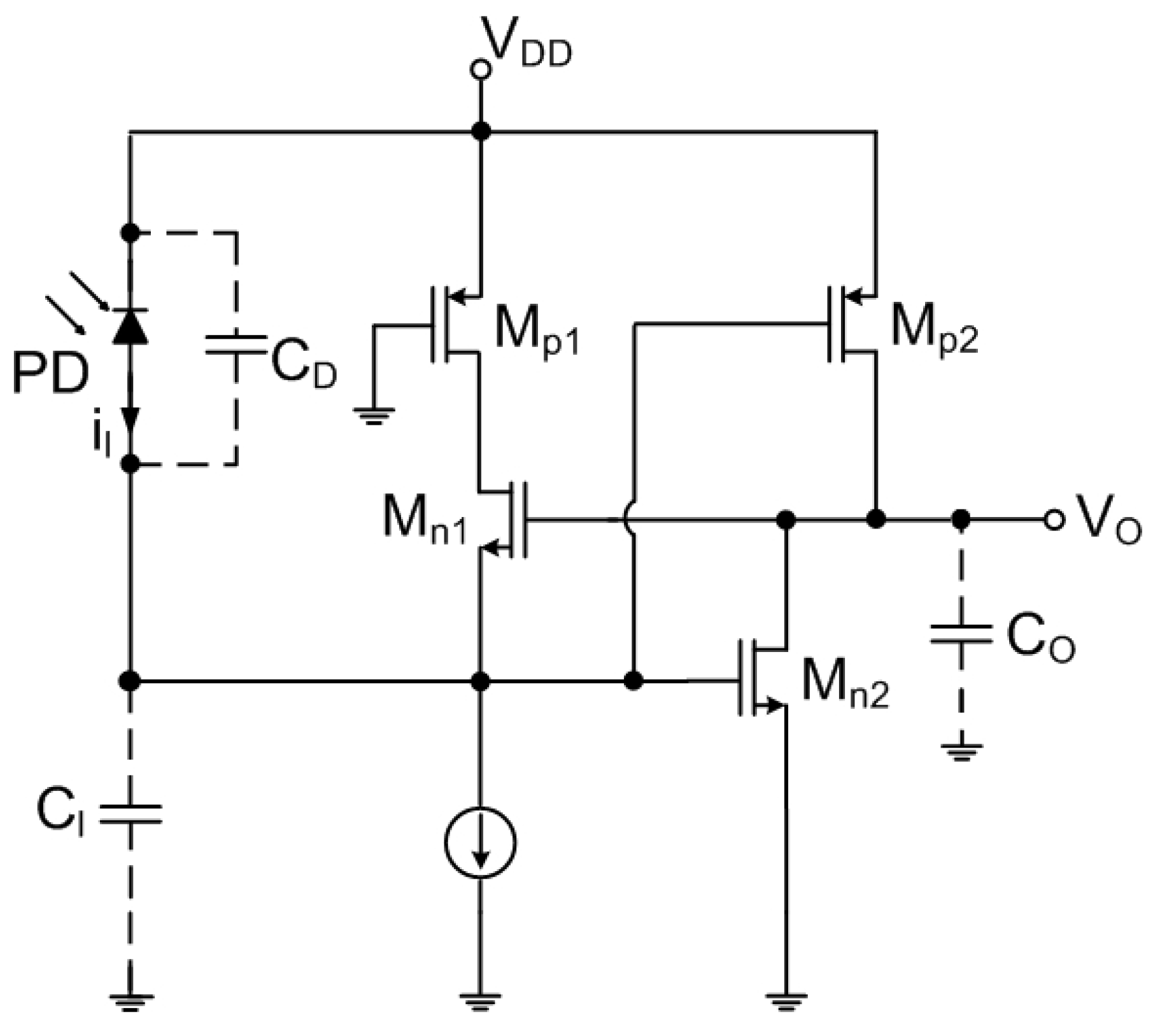
The seminal work of [
33] and the subsequent works of Shahdoost employed a CF approach with a CS input stage and a current-divider configuration, where the CS input stage was selected due to superior noise performance as elaborated in [
31]. Several practical modifications should have been done compared to a reference design shown in
Figure 7. For example, a PMOS current source was applied to the drain of the CS input-stage transistor and biased at the maximum possible gate-source voltage to minimize the thermal current noise. Furthermore, a cascode input stage was designed to improve the noise performance and to compensate for the Miller effect (The cascode eliminates the bandwidth degradation due to the Miller effect of the CS stage’s gate-drain capacitance. This degradation is particularly significant in CMOS circuits where the gate-drain capacitance can be as high as one third of the gate-source capacitance. The cascode also enhances the overall gain by increasing the stage’s output impedance [
4]). While an output buffer with on-chip inductor was added to extend the bandwidth and minimize possible phase distortions in [
33], the work [
31] employed an inductor-less approach with a source follower. Finally, a specially designed input bias networks have been added to limit the lower end of the amplifier’s bandwidth.
Although the approach does not contain an explicit integrator, the voltage amplifier output still follows the integral of the input current. Clearly, such design may be susceptible to instability and saturation problems and may suffer from the intolerance to DC input currents. All this necessitates a DC input current control circuit as was already reported in the original work of Razavi [
33] and further elaborated by Shahdoost. Although the results as reported by Shahdoost look extremely promising and have been mostly confirmed by experimental circuits using two different technologies, there may be certain issues that could impede a direct implementation of that circuit for low-power CMOS. Here the major concern is related to the problem of a voltage headroom which can manifest itself for circuits designed to run with lower than 2.2 V supply voltage reported in his most recent work. Furthermore, none of the works of Shahdoost including the most detailed one [
21] specified the value of the input and/or PD’s capacitance used for simulation and measurement characterization which makes it harder to position the design within the results of competing works as the results reported may be over-optimistic and the circuit performance with actual input capacitances may be significantly worse.
Both works of Razavi and Shahdoost addressed the problem of designing the TIA for optical communications. Different perspectives have been taken in [
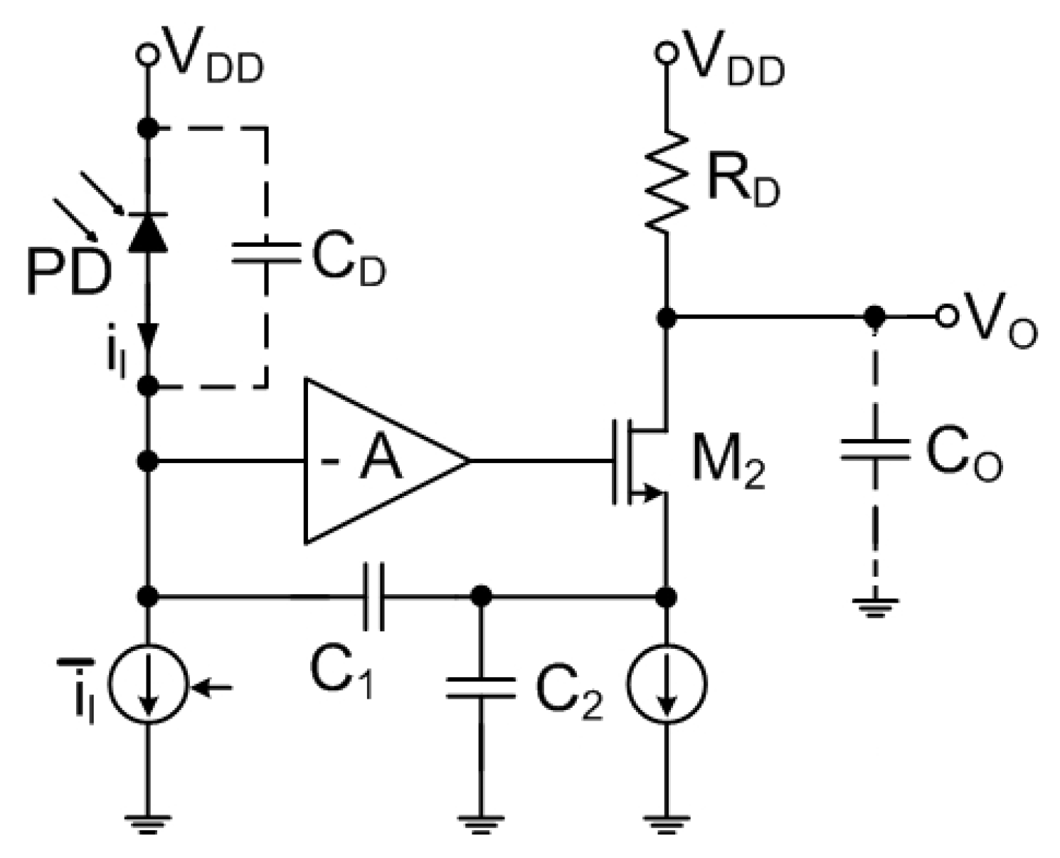
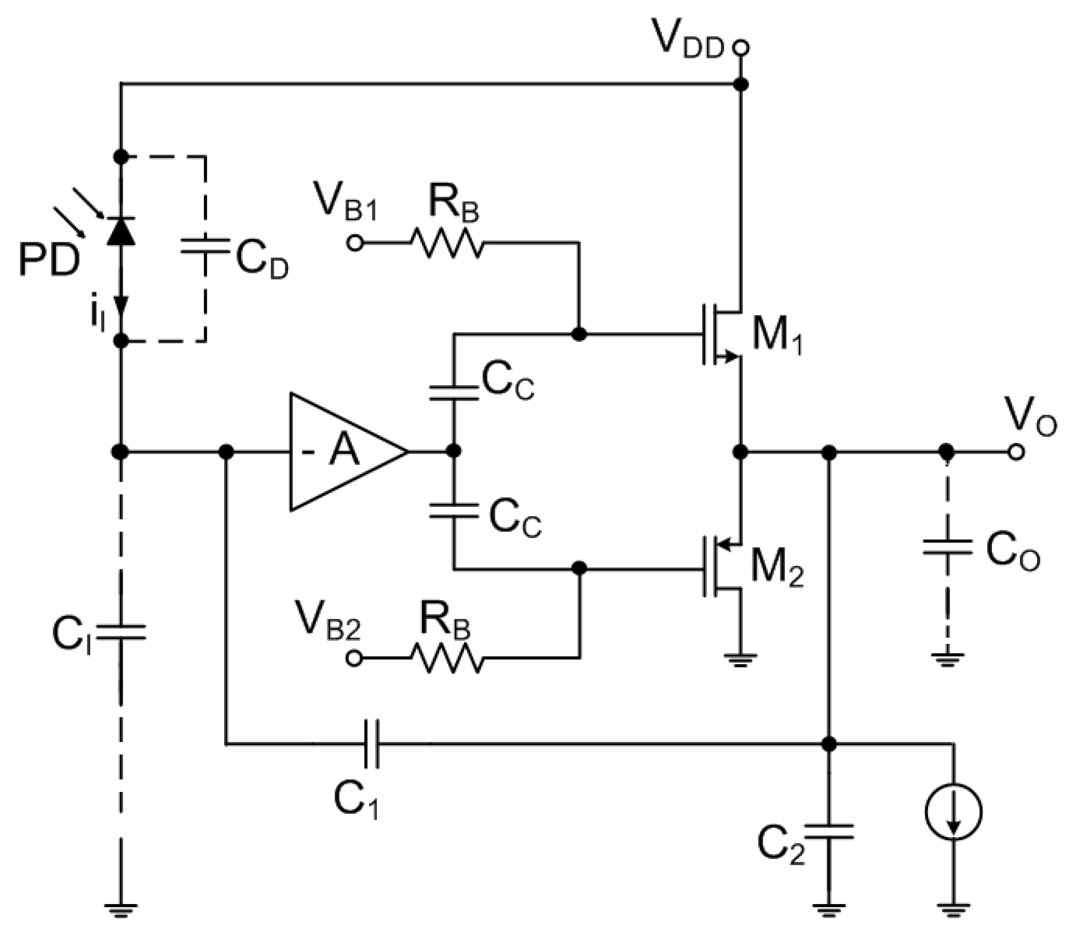
3], where the authors used the CF TIA to design a low-noise and highly linear TIA for miniaturized magnetic resonance imaging. The authors proposed a modification of the CF TIA where a push-pull buffer stage (see
Figure 8) is introduced when compared to vanilla CF TIA [
1]. The new approach eliminates the
as the current passing through
may be sensed by a low input impedance stage as the current-mode mixer or the
can be used for voltage mode operation. According to [
3], as the feedback also reduces the output impedance of the circuit, the noise currents of
and
are believed not to have significant contributions to the total noise figures. The push-pull architecture allows larger voltage swings which also help to reduce the input noise current as a smaller capacitance can be implemented for the given maximum value of the input current. According to [
3], the push-pull output stage can be also biased with a current smaller than the peak current delivered to the load, resulting in a lower power dissipation without affecting the linearity of the design. On the other hand, this buffer stage increases the capacitive loading of the voltage amplifier. Although this capacitive loading may be still acceptable for lower-frequency operations (generally below 150 MHz) such as MRI in [
3], this may be undesirable for higher-frequency applications close to 1 GHz range such as the envisioned OTDR.
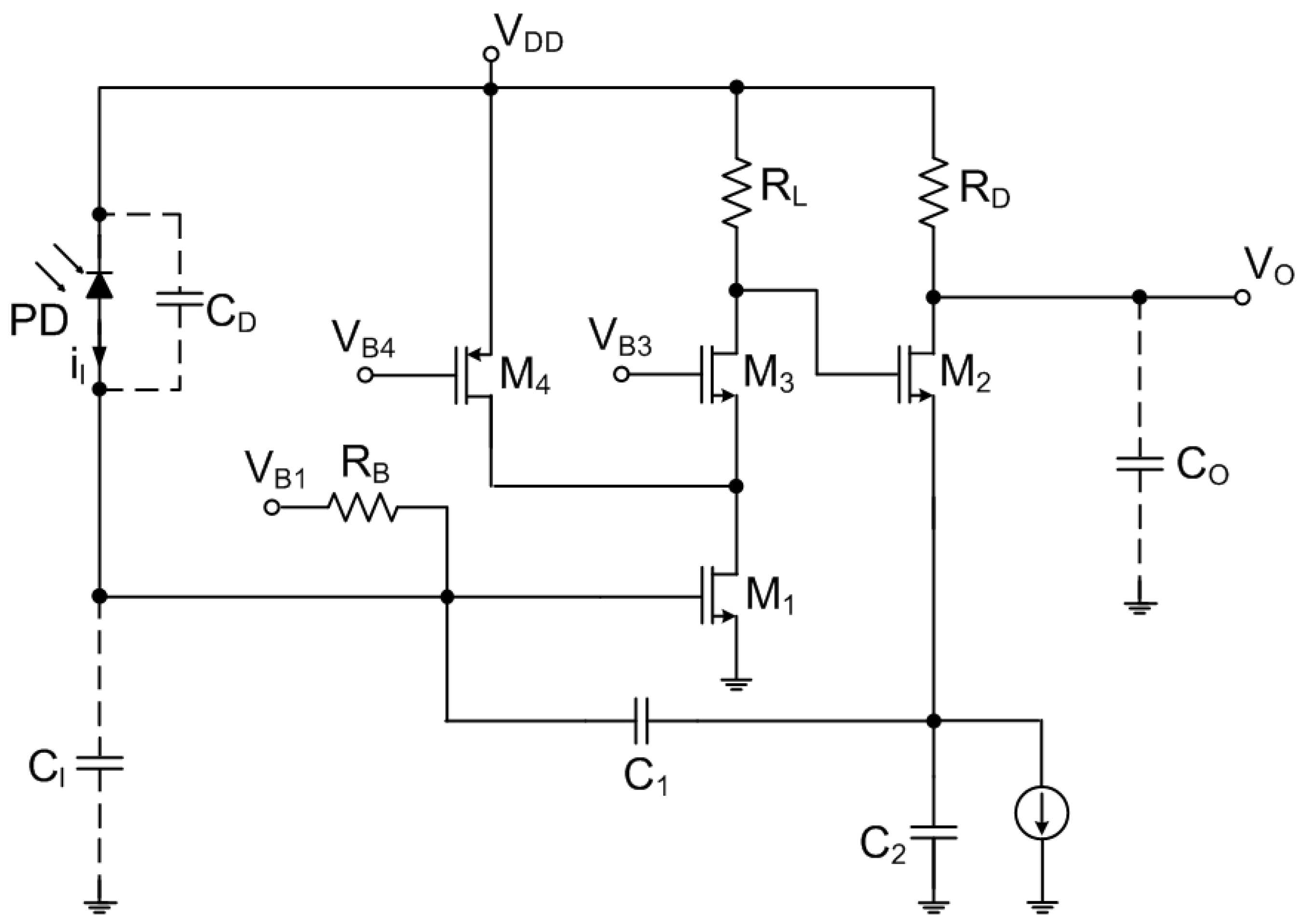
Considering all the trade-offs in CF TIA design, [
3] suggested to employ the voltage amplifier with the steering topology as shown in
Figure 9. Here the higher voltage gain is achieved by using
to provide 90% of the bias current needed for
allowing implementation of a large
, where the noise contribution of
is minimized by biasing it with a large overdrive voltage. The biasing voltage for
is generated by a current mirror while the biasing voltage for
is simply set to the lowest value that keeps the
in the saturation region during the operation. A careful examination reveals that this current steering topology with an additional
device is identical to the solution in the series of works of Shahdoost [
21]. Although the approach with push-pull buffer stage demonstrates a promising improvement in the linearity of the TIA, the transimpedance is inversely proportional to the frequency and, therefore, can be hardly used in the proposed form for wideband application such as OTDR.
Another promising approach was suggested in [
44], where a three-stage inverting amplifier TIA was proposed based on a noise-canceling concept (NC-TIA) (see
Figure 10). According to the authors, such NC-TIA shows approximately 15% reduction in the integrated input noise current when compared to the traditional three-stage inverter amplifier. Such a limited reduction is caused by the fact that the noise cancelation methods may only cancel the thermal noise and the flicker noise of the input MOSFET but cannot cancel the noise due to feedback resistor
. The authors managed to achieve an extremely good sensitivity with the FOM just slightly worse to that reported by Shahdoost.
The work [
15] provides one of the early examples of CMOS TIA design, where the CG input stage was selected to relax the trade-off between the bandwidth and the large PD capacitance (2.0 pF for the total input parasitic capacitance including ESD protection pad, etc. for DVI/HDMI applications). The authors have chosen the differential design to eliminate the common-mode noises with the subsequent two-cascaded voltage-gain stages designed as conventional CS differential amplifiers with active PMOS loads. Although the authors did not specifically target low-noise design, relatively poor noise performance of the circuit may again be attributed to the CG input stage. The presented results are obtained from the post-layout simulation and real circuit performance may have been slightly worse.
Around the same time, the same team also reported on a differential 12-Channel 60-Gb/s transimpedance amplifier array for optical printed circuit boards (OPCB) [
41]. The authors exploited again a CG input stage and applied an active feedback technique with negative capacitance compensation to obtain something which is currently known at RGC TIA, where the
was replaced by the MOSFET in triode mode. Although a classical CG input stage already has relatively small input impedance, according to the authors in [
41] this is insufficient to totally isolate the input capacitance due to poor device characteristics of conventional CMOS. The reported design showed extremely good results in terms of the FOM with the improved mainly achieved due to both increased gain and bandwidth, while the absolute noise figures remained rather poor. As with the design reported in [
15], this may be again attributes to relatively week noise performance of the input RGC stage.
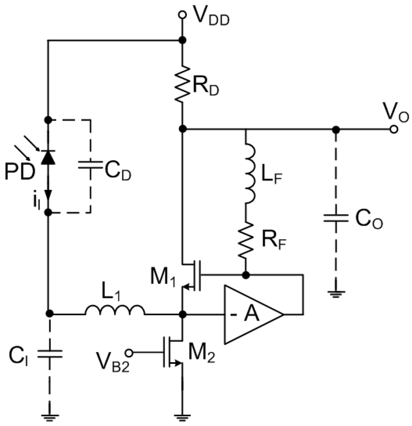
Similar RGC TIA was used as a basis in [
16], where the Cherry-Hooper technique was used to increase the bandwidth of the amplifier. Such modified RGC with local feedback is claimed to improve the regular RGC design. The authors introduced a feedback circuit (resistor in series with an inductor, see
Figure 11) which connects the gate to the drain of
in classical RGC. The modification not only improves the bandwidth of the amplifier, but also partially addresses a problem of the voltage headroom and decreases the input-referred noise. Moreover, a series inductor
had been also added for further bandwidth improvement and noise reduction. The implemented TIA is followed by a three-stage CS buffer with shunt peaking inductors used to enhance their bandwidth and a matching network. Interestingly, the amplifier itself draws only 8.2 mW out of the total power consumption reported for the circuit, while the rest 31.5 mW being consumed by the buffers. According to [
16], another important advantage of the approach is an improved biasing of the transistors. In the proposed modified RGC TIA the feedback resistor creates yet another path for the bias current of
through
, so that the voltage drop across
can be controlled by adjusting the current that flows through
. Thus,
can be increased to reduce even further the input-referred noise while sufficient DC current is provided to
by this additional path.
An interesting modification of a classical RGC TIA has been suggested in [
6,
39], where a low-power TIA (2 mW with a total power consumption including single-ended differential, pre-driver and driver circuits of 16 mW) was designed using an inverter with active common-drain feedback (ICDF) as shown in
Figure 12. A new design can be obtained from classical CS-based RGC TIA by replacing both resistors in CG main amplifier and CS local feedback with corresponding PMOS transistors. This inductor-less design allows achieving a large bandwidth of 8 GHz with approximately 28% reduction in current compared to the original RGC design. The impedance of the circuit is significantly lower compared to the standard RGC TIA as the inverter stage, in general, has larger gain than the CS amplifier stage from the conventional approach. The difference between the RGC and ICDF is that RGC outputs from the drain of the CG amplifier with the CS amplifier functioning as a local feedback stage, while the ICDF design takes the output from the inverter amplifier where the input stage operates as a local feedback stage. Hence, the transimpedance gain of the ICDF-TIA is larger than that of the classical RGC TIA designed for the same technology and similar performance constraints such as the same input impedance (see [
39] for details). The authors employed low-threshold transistors available in the 40nm CMOS process with the multi-threshold approach simultaneously enabling higher gain and adequate voltage headroom.
On the other hand, the conventional inverter-based TIA can have lower noise than the ICDF-TIA proposed in [
39] at the price of smaller bandwidth as the noise contribution due to active local feedback in ICDF-TIA is higher than the noise of the resistive feedback. The authors also show that the ICDF-TIA is also less sensitive to the supply noise when compared to classical RGC TIA. Still, the noise performance seems to remain a major drawback of the proposed design, as it is for classical RGC TIA circuits.
Similar good noise performance was also achieved with a multiple inductive-series technique in [
30], where the proposed wideband architecture consisted of the inverter gain stages as shown in
Figure 3 with on-chip inductors deployed between them. Here the deployed inductors with the parasitic capacitances resemble a third-order LC-ladder filter to perform an impedance transformation network. Obviously, the technique also allows absorption of the PD’s capacitance as a part of the impedance transformation network. The authors also claimed that the series approach manifests larger bandwidth enhancement and less sensitivity to an on-chip inductor quality factor when compared to more classical shunt-peaking techniques [
30].
A wideband CMOS TIA based on a combined series/shunt inductive peaking was reported in [
37]. The solution consisted of two stages, where the first pre-amplifier stage is a typical SFB TIA based on CS cascode. Here the source follower was used for the unilateral feedback with the post-amplifier composed of the cascode amplifier and the source follower. The shunt inductive peaking was applied to both the pre- and the post-amplifier with the inter-stage inductor inserted to split the capacitance from the transistors.
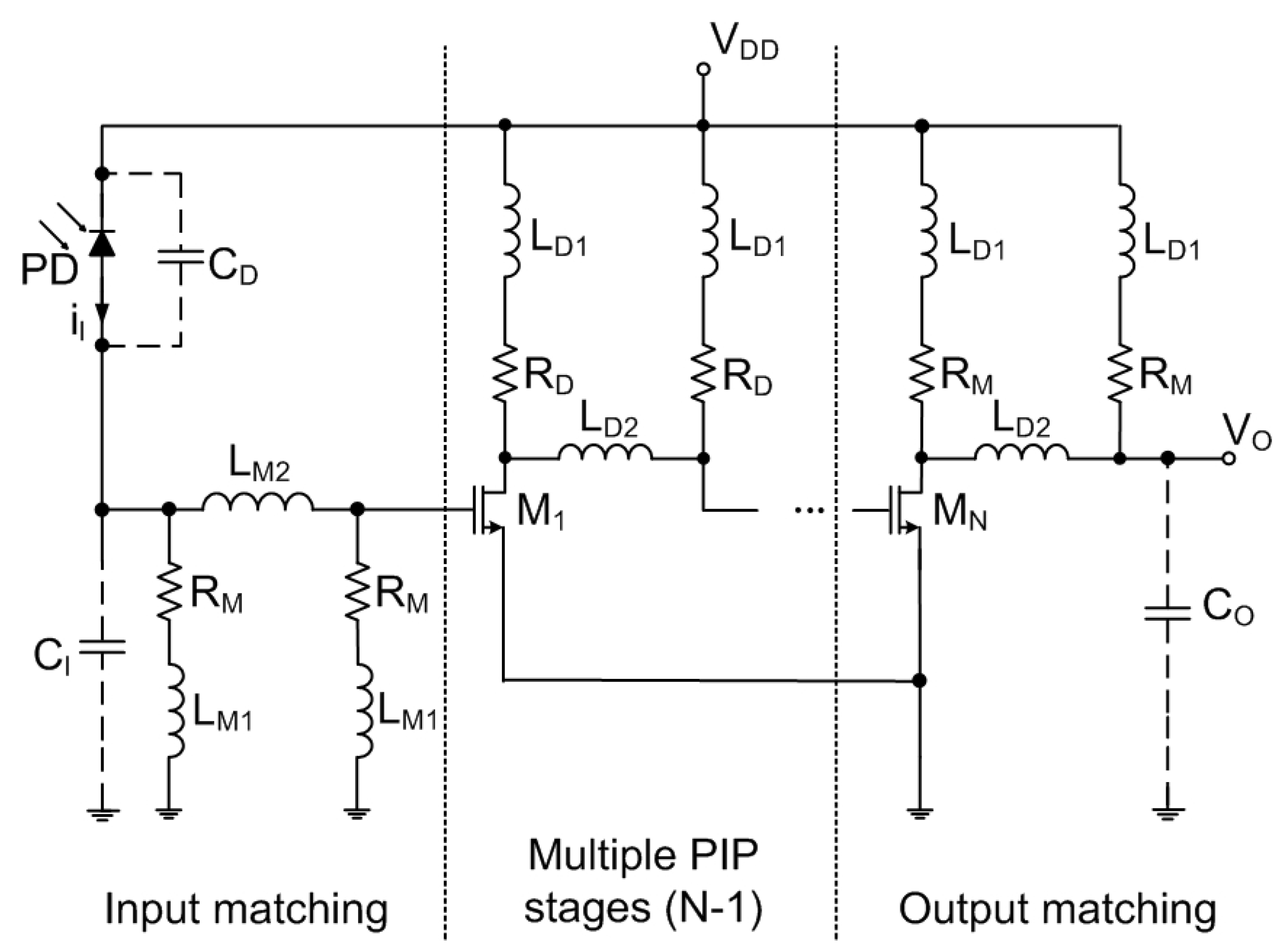
Further attempts to push the bandwidth of the TIA with inductive peaking have been reported in [
9,
36,
38], where limitations of the classical CS stages have been addressed with the PIP approach (see
Figure 13). The works [
9,
38] reported a TIA for 40 Gb/s applications composed of four cascaded CS stages with identical resistances for drain biasing resistors employed in each stage, while the input and output impedances are matched through the dedicated matching resistors
. It is worth mentioning that the
which is also one of the main limitations of the bandwidth in TIA, can also be effectively resonated by the proposed PIP configuration. Although this design provides an excellent gain-bandwidth product and good power consumption, the reported measured results on transimpedance showed significant non-flatness far bigger than 3 dB claimed by the authors. It is interesting to note here that although the design supports extremely large bandwidth of >30 GHz, the computed FOM is rather small. This is caused by relatively small
supported by design (50 fF for this high-speed application), moderate gain and relatively high noise. In 2008 a design for 10 Gb/s was reported by the same authors containing six CS stages with PIP. Although the latter design demonstrated an improvement in flatness and operated with
of 450 fF, no clear statement on the noise figures was provided.
An interesting design idea had been reported by [
26], where a classical RGC TIA was modified to have both the inductive shunt peaking and inductive gate peaking. The vertically stacked coupled inductors have been introduced by the author to enhance the bandwidth via the creation of complex poles. As the stacked inductors allow reduction of the area, the method introduces a relatively large coupling between both inductors and this coupling needs to be considered in the design. The author in [
26] also paid additional attention to the stability conditions in such advanced TIA. Unfortunately, even such an optimized architecture resulted in significant chip size compared to inductor-less designs (100 µm × 100 µm), while the noise numbers are also relatively high due to properties of the RGC stage as discussed before. The latter can be partially explained by the increased noise contribution of the
due to the presence of the gate inductor. An advantage of the approach is that the design is relatively insensitive to the quality factor of both added inductors and very thin traces were used to produce high inductance per area to further reduce the chip size.
An attempt to use a broadband matching with classical RGC had been reported in [
42], where the matching network included the
, the inductance of the bond wire, the parasitic capacitance at the source of
and an additional inductance. Although here again the RGC was responsible for relatively large noise, the work provides a good practical example on how the bonding wire can be exploited as an element of the matching network. Please note that a precise value of the bonding inductance cannot be guaranteed due to the process variations (typically between 0.7 and 2 nH) and one may need to choose the additional inductance optimally for wider bandwidth with negligible gain peaking.
Even though the inductor peaking results in significant bandwidth improvement for high-speed CMOS TIAs, many works reported on attempts in improving the bandwidth using inductor-less TIA configurations. For example, the work [
10] suggested to use
N identical TIAs in a parallel configuration to boost the bandwidth while keeping the transimpedance gain constant. Clearly, the same PD and the same capacitance
are used to drive this parallel TIA. According to the authors, the assumption of an ideal adder would not significantly affect the results as it can be realized using common-source buffers at the output of each SFB TIA and by adding their currents through a single resistive load. Here the buffers need to have a gain of 1 and, therefore, they can have the bandwidth much higher than the TIA itself. As the number of the parallel TIA increases, the effective damping factor of a combined TIA decreases translating to more ringing in the step response of the amplifier. This overshoot in the time domain corresponds to the peaking in the frequency domain and resembles the effects from the inductive peaking technique as the bandwidth enhancement comes at the expense of an acceptable ringing of the step response. The difference is that while in inductive peaking the bandwidth improvement comes at a price of an extra chip area used for the inductors, in the configuration proposed the power consumption is sacrificed [
10]. A clear advantage of the proposed scheme is that it can be used for any TIA topology and the bandwidth enhancement can be achieved for any type of the core TIA. Unfortunately, a higher number of the core TIAs also results in higher input-referred noise so that in lieu of the noise, ringing and the power consumption performance one shall not use more than two or three amplifiers connected in parallel.
If the amplifier is designed for relatively low-frequency applications (e.g., 1–2 GHz) such as OTDR shown in
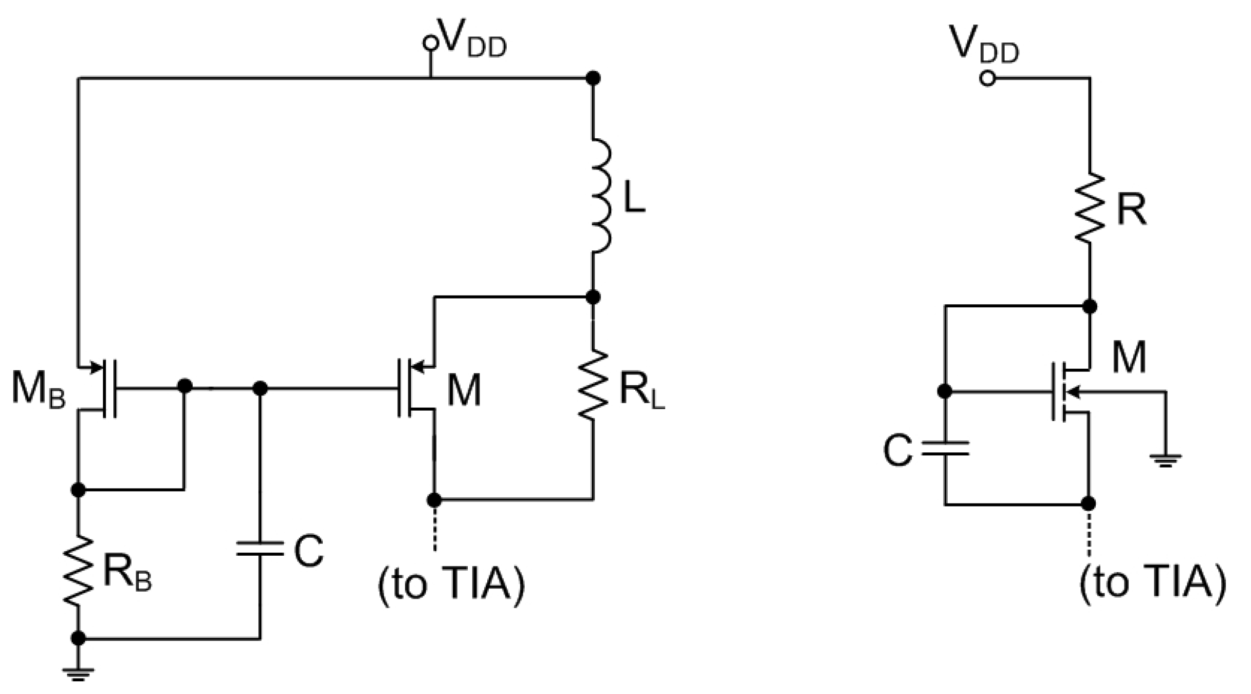
Table 1, not all inductive peaking configurations for bandwidth extension can be useful in practice. For example, if one tries to adopt a simple inductive shunt peaking, the required inductance can be very large unless the load resistor and the parasitic load capacitance are unrealistically small. In conventional shunt peaked (e.g., CS cascode) amplifier with a resistive load the maximum value of the output resistor is limited by the voltage drop across the resistor and the strategy as proposed in [
35] allows achievement of a higher gain when using a current source with inductive degeneration (see
Figure 14). As a result, a much smaller sized inductor is required when compared to a conventional shunt peaked approach. His approach achieves extremely good noise performance and the noise current density seems to be relatively flat over the frequency as detailed in [
35]. Several works have attempted to extend the bandwidth of the classical TIA topologies using the method of so-called active inductor peaking without inductance as shown in
Figure 14. A classical RGC TIA with resistive feedback as suggested by earlier works of [
34] was used by [
45] for designing a 1 GHz CMOS pre-amplifier with active inductor peaking to alleviate possible bandwidth degradation, while the work of [
11] instead employed a classical SFB TIA with resistive feedback, where the
of the CS stage was replaced by an identical active inductor configuration. Interestingly, the CS-based approach with active inductor load did not show a significant noise improvement when compared to RGC topology. The work [
45] also did not report on
value used for the measurements and both works employed a single-to-differential converter. It is worth mentioning that the work [
11] also adopted rather big
of 2 pF to model both the PD with large area suitable for lower-cost plastic optical fibers and significant input parasitic capacitance. According to [
11], the configuration not only allowed increase of the bandwidth but also resulted in approximately 15% decrease in noise when compared to classical SFB TIA with CS stage.
A similar active inductive peaking technique in combination with the capacitive degeneration was reported in [
43]. The authors employed an input RGC to reduce the input impedance, where an active inductive peaking and capacitive degeneration were used for the CS stage. Here, differently from [
11], the authors attempted to reduce the area and the parasitic capacitance of the resistor (see
Figure 14 (left)) by replacing the resistor
R with a MOSFET. The capacitive degeneration was applied to the source resistor of the CS stage to enhance the bandwidth via generating a zero to compensate the lowest pole.
A combination of several techniques had been suggested in [
7] to implement a TIA for 30 Gb/s communication link in 28 nm 1 V CMOS process. The authors addressed the problem by modifying the RGC TIA to have a 2-stage feedback amplifier, where the first CG stage shifts the voltage level at the input of the TIA closer to the supply voltage, while the second high-gain CS stage increases the gain in the loop. As with the previously discussed work [
16], here the authors also employed the Cherry-Hooper configuration to reduce the effect of the parasitic capacitance in
. Finally, an active inductor is used for bandwidth enhancement. This paper provides an excellent example that several circuit-level modifications of the reference TIA topologies may be needed to achieve the requirement performance with standard CMOS. Unfortunately, the results [
7] are provided without including
and no FOM may be computed (We cannot assume unknown value and use 0.5 pF as the author explicitly states that the
was not included).
The FOM-based performance of the reported CMOS TIA is shown in
Figure 15 in the form of dependency on the year the original publication. As expected, the CF TIA from Shahdoost has the highest FOM among the presented works. Please note that the logarithm of the FOM measure is provided and the second-best TIA from Oh [
41] is actually 1.5× worse in terms of FOM.
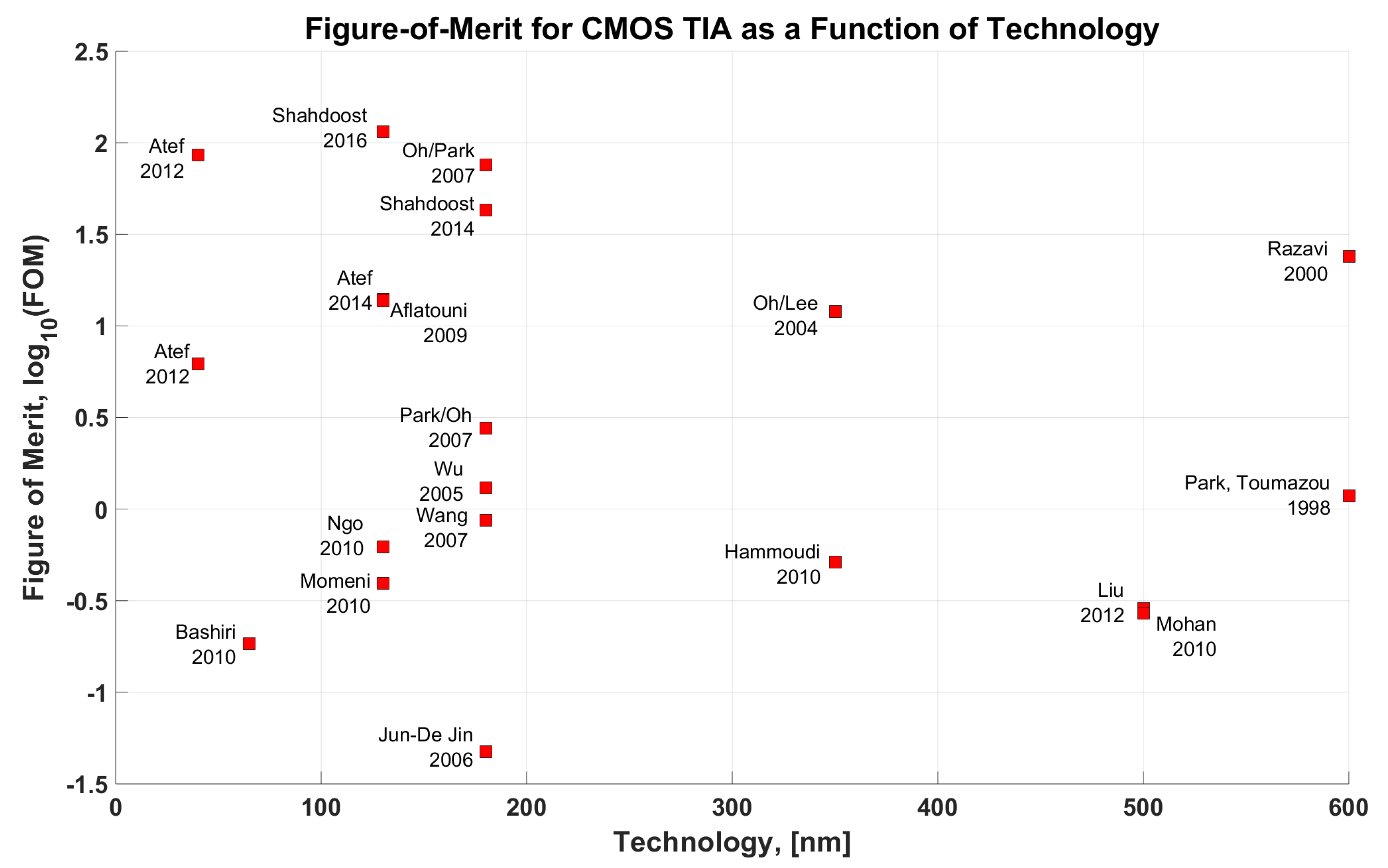
A complementary view on the evolution of the CMOS TIA in terms of suggested FOM is shown in
Figure 16, where the reported works are plotted depending on the technology node. A careful inspection of both works reveals that the work of Razavi [
33] can be considered to be an outlier in the sense that it seemed to perform better than one would expect from the year and technology. However, this will not be as surprising when one recalls that this was exactly the work which introduced the CF TIA.

