Abstract
Time-interleaved analog-to-digital converter (TI-ADC) technology can increase the sampling rate without changing resolution. But, the dynamic performance of TI-ADC system is seriously deteriorated by channel mismatches. Under the condition of large bandwidth, gain mismatch and timing mismatch vary with the frequency, which cannot be regarded as fixed values. To improve the dynamic performance of the TI-ADC system, an automatic calibration method of channel mismatches for wideband TI-ADC system is proposed in this article. Frequency-dependent channel mismatches are estimated by the algorithm based on sine fitting, and compensated by the means based on perfect reconstruction. The entire sampling and calculation process is automated and tedious operation is simplified. A 6.8-GS/s 12-bit wideband TI-ADC system is implemented. This sampling system can achieve SNDR (signal-to-noise and distortion ratio) above 49 dB and SFDR (spurious-free dynamic range) above 57 dB for an input signal from 100 MHz to 3300 MHz. The proposed calibration method improves the SNDR over 10 dB and the SFDR over 15 dB. The dynamic performance of the sampling system is close to that of its sub-ADC.
1. Introduction
The high-speed high-resolution sampling system is the crucial component in wideband digital receivers, measurement instruments, and communication systems [1,2]. The performance of the sampling system is mainly determined by analog-to-digital converters (ADCs), including sampling rate, dynamic performance and full power bandwidth. However, the contradiction between high sampling rate and high resolution restricts the development of ADCs [3]. TI-ADC technology can effectively solve this problem. Several ADCs with lower sampling rate are used to acquire the signal in parallel at the same clock frequency but different clock phases [4,5,6,7]. Finally, the sampling sequences of sub-ADCs are combined as the output of the system to increase the sampling rate. An ideal architecture of an M-channel TI-ADC system is shown as in Figure 1.
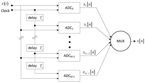
Figure 1.
The ideal model of an M-channel TI-ADC (Time-interleaved analog-to-digital converter) system.
TI-ADC technique can multiply the sampling rate, but channel mismatches are introduced, mainly including offset mismatch, gain mismatch, and timing mismatch [5,6,7,8,9,10,11]. Channel mismatches can seriously degrade the spurious-free dynamic range (SFDR) and signal-to-noise and distortion ratio (SNDR) of the TI-ADC system. At present, a lot of work has been done to correct the channel mismatches. The TI-ADC channel mismatch calibration is mainly composed of two aspects, one is channel mismatch estimation, and the other is channel mismatch compensation [12].
Accurate estimation of channel mismatches is a key step in realizing calibration of TI-ADC channel mismatches. The current TI-ADC mismatch estimation algorithm is mainly divided into two categories: forward estimation and backward estimation. Channel mismatches are calculated according to a calibration signal by the forward estimation algorithm in [13,14]. Channel mismatch measurement is with high stability and high accuracy using this kind of estimation method. However, if the channel parameters change, it is necessary to re-enter the calibration signal to calculate the channel mismatches. The advantage of backward estimation algorithm is that the signal is reconstructed directly from the acquired original signal without prior input of the calibration signal [15,16]. Although the backward estimation algorithm can evaluate the variation of channel mismatch in real time, it has high complexity and low precision. And the input signal should have certain special requirements, such as to have a generalized stationary characteristic, or to meet oversampling. Adding an additional reference channel to the TI-ADC system to estimate the channel mismatches is proposed in [17,18,19]. The disadvantage of this method is that extra channel which consumes more area and power increases the complexity of TI-ADC system. A series of sampled sinusoidal signals are used to estimate the amplitude response and phase response of each channel, and the frequency response of the entire frequency band is obtained by sine-wave fitting [20]. The disadvantage of this method is that it consumes a lot of measurement time, especially for wideband TI-ADC system with a large number of channels.
The purpose of TI-ADC channel mismatch compensation is to make the dynamic performance of TI-ADC system as close as possible to that of its sub-ADC. According to whether the channel parameters on the analog signal path need to be adjusted, channel mismatch compensation methods can be divided into mixed-signal compensation and full digital compensation [21,22,23]. An analog variable delay line (VDL) in the clock path of each sub-ADC is adopted to compensate the timing mismatch in mixed-signal compensation method. The front-end analog circuit needs to be changed when the mixed-signal compensation method is adopted, which will result in inflexibility in application. The full digital compensation method is more flexible and can compensate for all kinds of channel mismatches [22,23,24,25,26]. In [22], pseudo-aliasing signals are adopted to compensate gain and timing mismatches. A notch filter and feedback signals are used to estimate gain and timing mismatches, which increase its complexity. In [23], a derivative filter followed by a fractional delay filter and a scaling factor is exploited for timing mismatch calibration. In [24], a low-complexity Lagrange interpolation filter is used to compensate timing mismatch. But in these articles, gain mismatch is regarded as a fixed value and not applicable to signals with large bandwidth. In [25,26] frequency-dependent channel mismatches are researched, and compensated by means of perfect reconstruction.
2. Calibration Method
There are several types of mismatches in the TI-ADC, but offset mismatch, gain mismatch, and timing mismatch have the greatest impact on dynamic performance, such as SNDR and SFDR. The inconsistency of channel parameters is mainly caused by signal power splitter, balun, track-and-hold circuit in ADC, and cable length. Under the condition of large bandwidth, the gain mismatch and timing mismatch of each channel will vary with frequency, which is enough to make the dynamic performance of the sampling system deteriorate seriously. Offset mismatch can be seen as not changing with the frequency of input signal. It can be easily estimated from the sub-ADC outputs and corrected by the subtraction processes [26]. So, the following discussion focuses on the estimation and compensation methods of frequency-dependent gain mismatch and timing mismatch.
The proposed wideband TI-ADC channel mismatch compensation method is based on the principle of perfect reconstruction. The correction accuracy is determined by the estimation accuracy of gain and timing skew. In practice, it is necessary to collect at least 100 sets of data at equal frequency intervals in the working frequency band to ensure the estimation accuracy. Sampling and processing hundreds of sets of data separately is quite time-consuming. Therefore, an automatic calibration method of channel mismatches for wideband TI-ADC system is proposed. Using this method, the finite impulse response (FIR) filter coefficients needed for compensation can be calculated automatically. The consumed time and tedious operation during the calibration process are reduced.
The flowchart of automatic calibration method in wideband TI-ADC system is shown in Figure 2. A signal generator that can be configured through Ethernet is needed in this method. The sampling rate of the TI-ADC system is . sets of sinusoidal sequence at the frequency is sampled at equal frequency intervals within . The initial value of the loop variable is set to 1. Set th frequency of the signal generator when . After the setup of signal generator is complete, wait for a second to stabilize the output of the signal generator. Then, start recording data and name this data file i.dat. When a direct memory access (DMA) is completed (the data file reaches 4 MB), the file record is ended. The loop variable and the loop is continued until . After sampling data, the acquired data is used to estimate the channel mismatches. This procedure starts with a read file loop. In every cycle, the amplitude and phase of each channel at each frequency are acquired by sine fitting method. According to the conjugate symmetry of the real signal frequency response, the channel mismatch function will be obtained. This process will be elaborated in Section 2.1. The reconstruction filter coefficient is calculated by the method in Section 2.2.
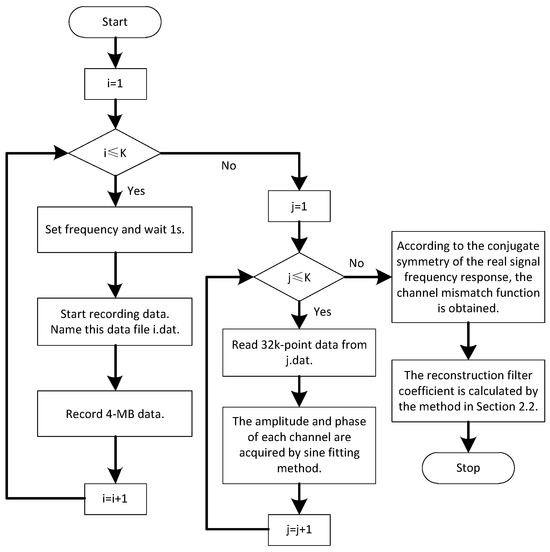
Figure 2.
Flowchart of automatic calibration method.
2.1. Estimation Method Based on Three-Parameter Least-Squares Fit to Sine-Wave Data
Any single-frequency sine wave expression can be written as
where is the sine wave frequency, is the amplitude, is the phase and is offset. According to the properties of trigonometric functions, Equation (1) can be rewritten to
where , , and .
Suppose that the sampling period of ADC is and sampling points are recorded as . , and can be obtained by solving the minimum value of Equation (3) by least square method [27]:
Thus, the amplitude, phase and offset of ADC at can be estimated from the sampled sinusoidal sequence.
Suppose that the TI-ADC system is M-channel. The aggregate sampling rate is . The sampling rate of each ADC is and the phase difference from ADC0 to ADCM−1 is in sequence. The frequency range of sampled signal is . Sine sequence of frequency points is acquired at equal frequency intervals in . Using the above sinusoidal three-parameter fitting estimation method, the amplitude discrete function and the phase discrete function of each channel at frequency points are obtained, where and .
Based on the amplitude discrete function and phase discrete function of channel 0, the gain discrete equation of each channel at frequency can be written as
and the phase difference discrete equation is
According to the conjugate symmetry of the real signal frequency response, the channel mismatch equation can be acquired by and :
where .
2.2. Compensation Method Based on Perfect Reconstruction
The perfect reconstruction structure diagram of M-channel TI-ADC system is shown in Figure 3. The equivalent transmission function of each channel before ADCs is regarded as , which corresponds to the estimated channel mismatch equation in Section 2.1. The sampling rate of each channel is of the aggregate sampling rate, which is equivalent to down sampling the signal . is sampling clock. After times up sampling, the discrete signals of each channel are sent to the digital compensation FIR filter . The output signal of each filter is combined and the compensated signal is obtained. In the following derivation, the coefficients of compensation FIR filters can be gotten using the perfect reconstruction algorithm.
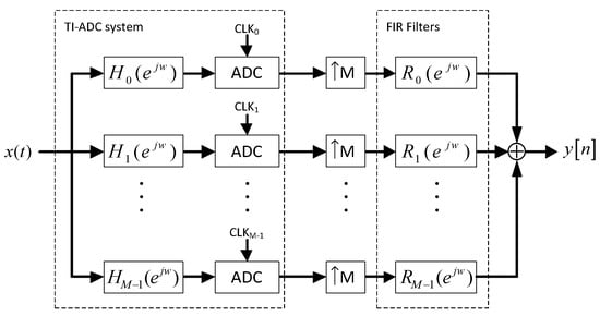
Figure 3.
Perfect reconstruction structure diagram of M-channel TI-ADC system.
The system sampling rate is and the sampling period . The bandwidth of input wideband signal satisfies . The output of the system in Figure 3 is
where . The signal is sampled in parallel by ADCs with a sampling rate of , which leads to aliasing of the spectrum. When , Equation (7) is the spectrum of the input signal. When , Equation (7) is the signal caused by aliasing, which should be eliminated. Equation (7) can also be written as:
where:
According to perfect reconstruction theory [28], if only gain and delay exist between input and output of the system, the following conditions should be satisfied:
The following matrix expressions can be obtained from Equations (9) and (10):
where , and
is a matrix composed of channel mismatch function , and is a matrix composed of compensation filter for each channel. The frequency response equation of the compensated filter can be obtained as
After transforming into the time domain, the imaginary part of its complex coefficient is very small and can be ignored. The corresponding coefficients of the compensation filter are
3. System Architecture
In order to verify the proposed calibration method, a TI-ADC system is described in this section. Four 1.7-GS/s sub-ADCs in two ADC chips are time-interleaved in this system. The system mainly consists of a field programmable gate array (FPGA) board, two sampling cards in the form of an FPGA Mezzanine card (FMC), a clock board, an input output (IO) board, a backplane, a receiving board and a storage server. The overall structure is shown in Figure 4. Analog signal is connected to a splitter and transmitted to FMCs respectively. The reference clock is connected to the clock board, and the sampling clock and SYSREF are generated to drive the FMC. The Joint Test Action Group (JTAG) interface can be connected to the computer for debug. Backplane is mainly used to power and interconnect the circuit boards. The sampled data can be passed to the back end via multi-gigabit transceiver (MGT), which is converted from electrical signal to optical signal by optical transceiver in IO board, and transmitted to receiving board of storage server through optical fiber. IO board implements the interface expansion of the FPGA board, which integrates two quad small form-factor pluggable (QSFP) optical transceivers and four small form-factor pluggable (SFP) optical transceivers. QSFP optical transceivers are used to transmit sampled data, and SFP optical transceivers can be used to receive control information. Storage of sampled data and TI-ADC channel mismatch compensation are carried out on the storage server. A receiving board with a peripheral component interconnect express (PCIE) interface is installed in the storage server. The receiving board integrates two QSFP optical transceivers for receiving sampled data from the optical fiber, and transmits it to the hard disks for storage.
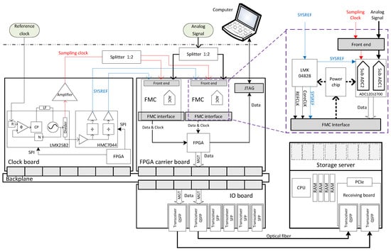
Figure 4.
Overall structure of the TI-ADC system.
A commercial ADC (ADC12DJ2700) is used to implement the 3.4-GS/s 12-bit FMC. The structure of the FMC is shown in the dotted box on the right of Figure 4. In the ADC chip, two sub-ADCs alternately sample data. The ADC chip has a maximum sample rate of 5.4 GS/s and a resolution of 12 bits. There is a variable delay line (VDL) in the clock path of each sub-ADC, which can be adopted to generate various phase required by TI-ADC systems. The ADC12DJ2700 operates in JMODE1. In this mode, two 1.7-GS/s sub-ADCs in the ADC chip are time-interleaved to double the sampling rate. Two 3.4-GS/s ADC chips are time-interleaved to double the sampling rate again. The delay time of ADC1 relative to ADC0 is one quarter of the sampling clock period, which is implemented by the Noiseless Aperture Delay Adjustment register in ADCs. The ADC uses SYSREF signal to achieve deterministic latency and multi-device synchronization. The Clock chip (LMK04828) works in 0-delay mode, and provides SYSREF for ADC and FPGA, Core CLK for JSED204B IP core, and REFCLK for MGT. The frontend circuit is used to implement single to differential conversion and impedance match for analog input and sampling clock. A broadband balun (BAL-0006SMG) is adopted to achieve a good balance and frequency response.
There is a high performance FPGA (XC7VX690T) integrated on the FPGA board, which is used to control sampling and receive data from ADCs. The board has two FMC interfaces to implement multi-channel high-speed serial communication between FPGA and FMC. Pre-processing such as data alignment is done in the FPGA. The data processed by FPGA can be delivered for storage via MGT or analysis via JTAG.
Clock jitter corresponds to the uncertainty of the sampling timing of the ADC during analog-to-digital conversion, and can usually be quantitatively characterized by measuring its root mean square (RMS) value. Signal-to-noise ratio (SNR) is an important index to evaluate the performance of an ADC. According to the relation between the jitter and SNR [29], the SNR can be estimated by Equation (14). If MHz and dB, the should be less than 150 fs.
The clock chip (LMX2582) meets the requirement of the sampling clock jitter. LMX2582 is a phase locked loop (PLL) which is used to generate a 1.7-GHz sampling clock and the external voltage-controlled oscillator (VCO) of another clock chip (HMC7044). The HMC7044 acts as a clock divider, dividing the 1.7-GHz clock to 5-MHz SYSREF. Both clock chips are controlled by FPGA via the serial peripheral interface (SPI).
4. Results and Discussion
In order to verify the automatic calibration method proposed in this article, the wideband TI-ADC system designed in Section 3 is used for testing. A four-channel TI-ADC system is implemented using four sub-ADCs in two chips. The test setup is shown in Figure 5. The 100-MHz reference clock to the clock board is produced by a signal generator (SMJ100A). The single frequency sine wave is produced by another signal generator (E8257D). The sine wave is sent to two FMCs through a power splitter. The 1.7-GHz sampling clock generated by the clock board is delivered to two FMCs through another power splitter. The sampled data is transferred to the storage server through QSFP optical transceivers on the IO board. Data storage and TI-ADC channel mismatch calibration are completed in the storage server. The storage server and E8257D are connected via Ethernet. Custom software running on the storage server can configure the E8257D through Ethernet.
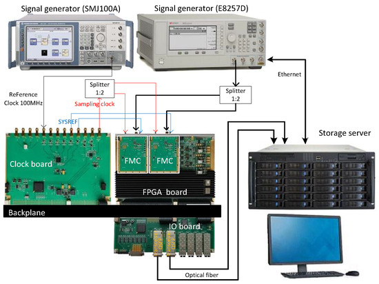
Figure 5.
Experimental setup for four-channel 6.8-GS/s TI-ADC system.
Data acquisition is controlled by software running on the storage server. The frequency range of calibration data is from 100 MHz to 3300 MHz and the frequency interval is 20 MHz. The frequency band 0~100 MHz and 3300~3400 MHz are not of concern, and the gain and phase of these frequency bands can be directly replaced by that of 100 MHz and 3300 MHz, respectively. Calibration is done on MATLAB. After the software is started, the entire process is automatically completed by the sampling system and signal generator. Curves of magnitude versus frequency relative to channel 0 are shown in Figure 6a, and that of phase is shown in Figure 6b. From the amplitude-frequency and phase-frequency curves of four sub-ADCs, it can be seen that the sub-ADCs in the same chip have better consistency. But there are still deviations in some frequency ranges. These deviations still deteriorate the dynamic performance of the system.
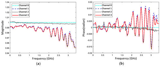
Figure 6.
Curves of four channels: (a) magnitude vs. frequency; (b) phase vs. frequency.
From [30] we can see that, there are spurs at when gain and timing mismatch exist, where is sampling rate of system, is the number of ADC, is frequency of input sinusoidal signal and . The output spectrum of 2.81 GHz sinusoidal signal before and after compensation is shown in the Figure 7. In this sampling system, GS/s, and . Due to the existence of gain mismatch and phase mismatch, spurs appear in the spectrum at 0.59 GHz, 1.11 GHz and 2.29 GHz. The spurs caused by mismatches are significantly suppressed after calibration. The SFDR is increased from 37.7 dB to 61.6 dB and SNDR is raised from 37.4 dB to 50.3 dB.
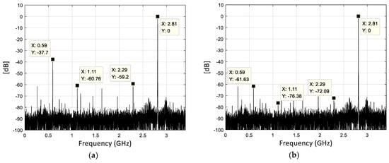
Figure 7.
The spectrum of 2.81 GHz sinusoidal signal: (a) before calibration; (b) after calibration.
A multi-tone power ratio (MTPR) test is performed in the TI-ADC system. The input frequency range of multi-tone sinusoidal signal is from 810 MHz to 3210 MHz and the interval is 200 MHz. The output spectrum of multi-tone signal before and after compensation is shown in the Figure 8. Comparing Figure 8a with Figure 8b, the spurious signals due to channel mismatches are effectively suppressed after calibration.
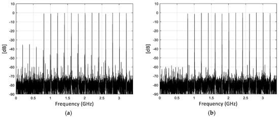
Figure 8.
The spectrum of multi-tone signal: (a) before calibration; (b) after calibration.
The measured SFDR and SNDR versus frequency before and after calibration are plotted in Figure 9. The SNDR above 49 dB and SFDR above 57 dB for a sinusoidal input signal from 100 MHz to 3300 MHz can be obtained after calibration by this TI-ADC system. The SNDR is improved over 10 dB and the SFDR is increased by more than 15 dB. Dynamic performance comparison between the TI-ADC system and its sub-ADC is depicted in Figure 10. The dynamic performance of the TI-ADC system is close to that of its sub-ADC, which shows the validity of the proposed method.
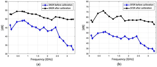
Figure 9.
Test result before and after calibration: (a) SNDR; (b) SFDR.
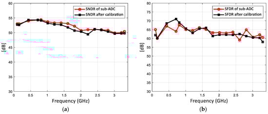
Figure 10.
Comparison between the TI-ADC system and its sub-ADC: (a) SNDR; (b) SFDR.
There are many methods to compensate channel mismatches in TI-ADC systems. The calibration algorithms in [31,32] and this work are compared. Dynamic performance comparison among the methods in [31,32] and this article is shown in Figure 11. The method in [31] regards gain mismatch and time mismatch as not changing with frequency. When multiple chips are time-interleaved, it works only if the input signal is narrowband. As the frequency increases, the dynamic performance of the TI-ADC system decreases rapidly. In [32], a Lagrange interpolator is used as the reconstruction filter to correct timing mismatch. This method cannot effectively correct the frequency-dependent gain mismatch. It can be seen from the Figure 11 that the proposed calibration method is superior to that in [31,32].
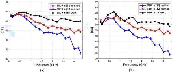
Figure 11.
Comparison among the methods in [31,32] and this article: (a) SNDR; (b) SFDR.
5. Conclusions
In this article, an automatic calibration method of channel mismatches for wideband TI-ADC system is proposed. Frequency-dependent channel mismatches are estimated by the method based on sine fitting, and compensated by the method based on perfect reconstruction. The entire sampling and calculation process is automated and tedious operation is simplified. A 6.8-GS/s 12-bit wideband sampling system hardware is designed to verify the proposed method. Although there are frequency-dependent gain and timing mismatches between each channel, the coefficients of the compensation filter can be easily obtained by using the proposed calibration method. This sampling system can achieve SNDR above 49 dB and SFDR above 57 dB for an input signal from 100 MHz to 3300 MHz. The SNDR is improved over 10 dB and the SFDR is increased by more than 15 dB. The dynamic performance of the sampling system is close to that of its sub-ADC. The experimental results show the validity of the proposed method.
Author Contributions
Data curation, J.L. and J.P.; Formal analysis, J.L. and Y.Z.; Methodology, J.L.; Software, Y.Z.; Validation, J.L.; Writing—original draft, J.L.; Writing—review & editing, J.P. and Y.Z.
Funding
This research received no external funding.
Conflicts of Interest
The authors declare no conflict of interest.
References
- Fang, J. A 5-GS/s 10-b 76-mW Time-Interleaved SAR ADC in 28 nm CMOS. IEEE Trans. Circuits Syst. I Regul. Pap. 2018, 64, 1673–1683. [Google Scholar] [CrossRef]
- Singh, S.; Anttila, L.; Epp, M.; Schlecker, W.; Valkama, M. Frequency Response Mismatches in 4-channel Time-Interleaved ADCs: Analysis, Blind Identification, and Correction. IEEE Trans. Circuits Syst. I Regul. Pap. 2015, 62, 2268–2279. [Google Scholar] [CrossRef]
- Li, J.; Wu, S.; Liu, Y.; Ning, N.; Yu, Q. A Digital Timing Mismatch Calibration Technique in Time-Interleaved ADCs. IEEE Trans. Circuits Syst. II Express Briefs 2014, 61, 486–490. [Google Scholar] [CrossRef]
- Monsurrò, P.; Rosato, F.; Trifiletti, A. New Models for the Calibration of Four-Channel Time-Interleaved ADCs Using Filter Banks. IEEE Trans. Circuits Syst. II Express Briefs 2018, 65, 141–145. [Google Scholar] [CrossRef]
- Black, W.C.; Hodges, D.A. Time interleaved converter arrays. IEEE J. Solid-State Circuits 1980, 15, 1022–1029. [Google Scholar] [CrossRef]
- Xu, S.; Lim, Y.C.; Lee, J.W. Recursive Filters for Time-Interleaved ADC Mismatch Compensation. IEEE Trans. Circuits Syst. I Regul. Pap. 2016, 63, 848–858. [Google Scholar] [CrossRef]
- Reyes, B.T.; Sanchez, R.M.; Pola, A.L.; Hueda, M.R. Design and Experimental Evaluation of a Time-Interleaved ADC Calibration Algorithm for Application in High-Speed Communication Systems. IEEE Trans. Circuits Syst. I Regul. Pap. 2017, 64, 1019–1030. [Google Scholar] [CrossRef]
- Buchwald, A. High-speed time interleaved ADCs. IEEE Commun. Mag. 2016, 54, 71–77. [Google Scholar] [CrossRef]
- Monsurrò, P.; Trifiletti, A. Calibration of Time-Interleaved ADCs via Hermitianity-Preserving Taylor Approximations. IEEE Trans. Circuits Syst. II Express Briefs 2017, 64, 357–361. [Google Scholar] [CrossRef]
- Lin, C.; Wei, Y.; Lee, T. A 10-bit 2.6-GS/s Time-Interleaved SAR ADC with a Digital-Mixing Timing-Skew Calibration Technique. IEEE J. Solid-State Circuits 2018, 53, 1508–1517. [Google Scholar] [CrossRef]
- Kang, H.; Hong, H.; Park, S.; Kim, K.; Ahn, K.; Ryu, S. A Sign-Equality-Based Background Timing-Mismatch Calibration Algorithm for Time-Interleaved ADCs. IEEE Trans. Circuits Syst. II Express Briefs 2016, 63, 518–522. [Google Scholar] [CrossRef]
- Mafi, H.; Yargholi, M.; Yavari, M. Digital Blind Background Calibration of Imperfections in Time-Interleaved ADCs. IEEE Trans. Circuits Syst. I Regul. Pap. 2017, 64, 1504–1514. [Google Scholar] [CrossRef]
- Chen, H.; Lee, J.; Chen, J. Digital background calibration for timing mismatch in time-interleaved ADCs. Electron. Lett. 2006, 42, 74–75. [Google Scholar] [CrossRef]
- Pereira, J.M.D.; Girao, P.M.B.S.; Serra, A.M.C. An FFT-based method to evaluate and compensate gain and offset errors of interleaved ADC systems. IEEE Trans. Instrum. Meas. 2004, 53, 423–430. [Google Scholar] [CrossRef]
- Liu, S.; Lv, N.; Ma, H.; Zhu, A. Adaptive semiblind background calibration of timing mismatches in a two-channel time-interleaved analog-to-digital converter. Analog Integr. Circuits Signal Process. 2017, 90, 1–7. [Google Scholar] [CrossRef]
- Liu, S.J.; Qi, P.P.; Wang, J.S.; Zhang, M.H.; Jiang, W.S. Adaptive Calibration of Channel Mismatches in Time-Interleaved ADCs Based on Equivalent Signal Recombination. IEEE Trans. Instrum. Meas. 2014, 63, 277–286. [Google Scholar] [CrossRef]
- Centurelli, F.; Monsurrò, P.; Trifiletti, A. Efficient Digital Background Calibration of Time-Interleaved Pipeline Analog-to-Digital Converters. IEEE Trans. Circuits Syst. I Regul. Pap. 2012, 59, 1373–1383. [Google Scholar] [CrossRef]
- Liu, W.; Chiu, Y. Time-Interleaved Analog-to-Digital Conversion with Online Adaptive Equalization. IEEE Trans. Circuits Syst. I Regul. Pap. 2012, 59, 1384–1395. [Google Scholar] [CrossRef]
- Centurelli, F.; Monsurrò, P.; Trifiletti, A. Improved Digital Background Calibration of Time-Interleaved Pipeline A/D Converters. IEEE Trans. Circuits Syst. II Express Briefs 2013, 60, 86–90. [Google Scholar] [CrossRef]
- Zhao, L.; Hu, X.; Feng, C.; Tang, S.; Liu, S.; An, Q. A 1.6-Gsps High-Resolution Waveform Digitizer Based on a Time-Interleaved Technique. IEEE Trans. Nucl. Sci. 2013, 60, 2180–2187. [Google Scholar] [CrossRef]
- Chen, S.; Wang, L.; Zhang, H.; Murugesu, R.; Dunwell, D.; Carusone, A.C. All-Digital Calibration of Timing Mismatch Error in Time-Interleaved Analog-to-Digital Converters. IEEE Trans. Very Large Scale Integr. (VLSI) Syst. 2017, 25, 2552–2560. [Google Scholar] [CrossRef]
- Matsuno, J.; Yamaji, T.; Furuta, M.; Itakura, T. All-Digital Background Calibration Technique for Time-Interleaved ADC Using Pseudo Aliasing Signal. IEEE Trans. Circuits Syst. I Regul. Pap. 2013, 60, 1113–1121. [Google Scholar] [CrossRef]
- Khan, S.R.; Hashmi, A.A.; Choi, G. A fully digital background calibration technique for M-channel time-interleaved ADCs. Circuits Syst. Signal Process. 2016, 36, 3303–3319. [Google Scholar] [CrossRef]
- Schmidt, C.A.; Cousseau, J.E.; Figueroa, J.L.; Reyes, B.T.; Hueda, M.R. Efficient Estimation and Correction of Mismatch Errors in Time-Interleaved ADCs. IEEE Trans. Instrum. Meas. 2016, 65, 243–254. [Google Scholar] [CrossRef]
- Munkyo, S.; Rodwell, M.J.W.; Madhow, U. Comprehensive digital correction of mismatch errors for a 400-msamples/s 80-dB SFDR time-interleaved analog-to-digital converter. IEEE Trans. Microw. Theory Tech. 2005, 53, 1072–1082. [Google Scholar] [CrossRef]
- Lim, Y.C.; Zou, Y.; Lee, J.W.; Chan, S. Time-Interleaved Analog-to-Digital-Converter Compensation Using Multichannel Filters. IEEE Trans. Circuits Syst. I Regul. Pap. 2009, 56, 2234–2247. [Google Scholar] [CrossRef]
- Renczes, B.; Kollár, I.; Dabóczi, T. Efficient Implementation of Least Squares Sine Fitting Algorithms. IEEE Trans. Instrum. Meas. 2016, 65, 2717–2724. [Google Scholar] [CrossRef]
- Velazquez, S.R.; Nguyen, T.Q.; Broadstone, S.R. Design of hybrid filter banks for analog/digital conversion. IEEE Trans. Signal Process. 1998, 46, 956–967. [Google Scholar] [CrossRef]
- Awad, S.S.; Wagdy, M.F. More on jitter effects on sinewave measurements. IEEE Trans. Instrum. Meas. 1991, 40, 549–552. [Google Scholar] [CrossRef]
- Kurosawa, N.; Kobayashi, H.; Maruyama, K.; Sugawara, H.; Kobayashi, K. Explicit analysis of channel mismatch effects in time-interleaved ADC systems. IEEE Trans. Circuits Syst. I Fundam. Theory Appl. 2001, 48, 261–271. [Google Scholar] [CrossRef]
- Yang, K.; Kong, X.; Shi, J.; Ye, P. Mathematical Statistics and Spectrum Analysis Calibration Method for Time-Interleaved ADC System. J. Univ. Electron. Sci. Technol. China 2018, 47, 43–50. [Google Scholar] [CrossRef]
- Abbaszadeh, A.; Aghdam, E.N.; Rosado-Muñoz, A. Low complexity digital background calibration algorithm for the correction of timing mismatch in time-interleaved ADCs. Microelectron. J. 2018, 81, 1–11. [Google Scholar] [CrossRef]
© 2019 by the authors. Licensee MDPI, Basel, Switzerland. This article is an open access article distributed under the terms and conditions of the Creative Commons Attribution (CC BY) license (http://creativecommons.org/licenses/by/4.0/).