1. Introduction
Multilevel topology is widely used in high-power and high-voltage applications due to its lower total harmonic distortion (THD), lower filter size, and lower switching losses in each switching device than those of the conventional two-level PWM converters and inverters [
1]. Each use of multilevel topology increases the number of voltage levels, making the output voltage even closer to the sinusoidal wave and reducing the harmonic distortion [
2,
3]. Among the various multilevel topologies, the cascaded NPC/H-bridge (CNHB) topology is advantageous in that it is easier to increase the output voltage levels and modularity than it is through the use of other topologies such as cascaded H-bridge (CHB), neutral-point clamped (NPC), and flying capacitor (FC) [
4,
5,
6].
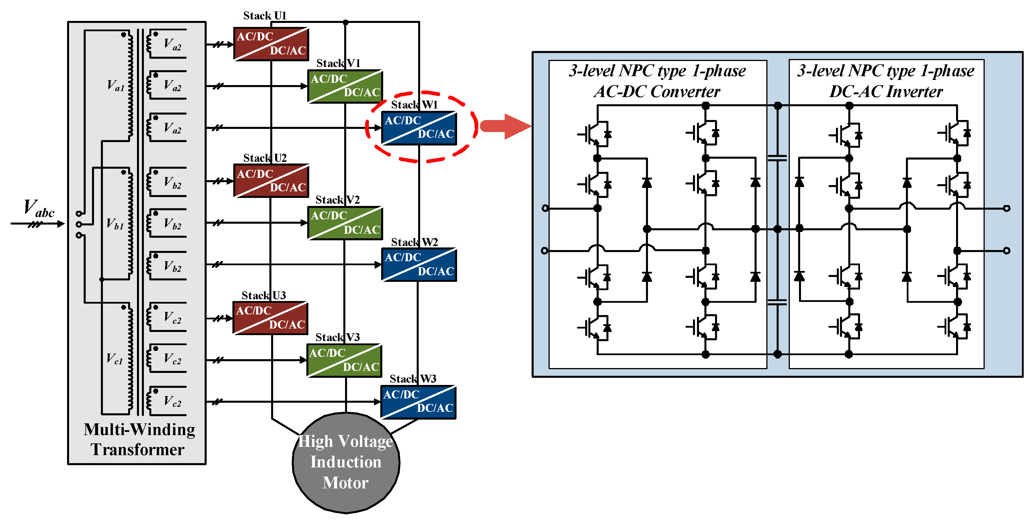
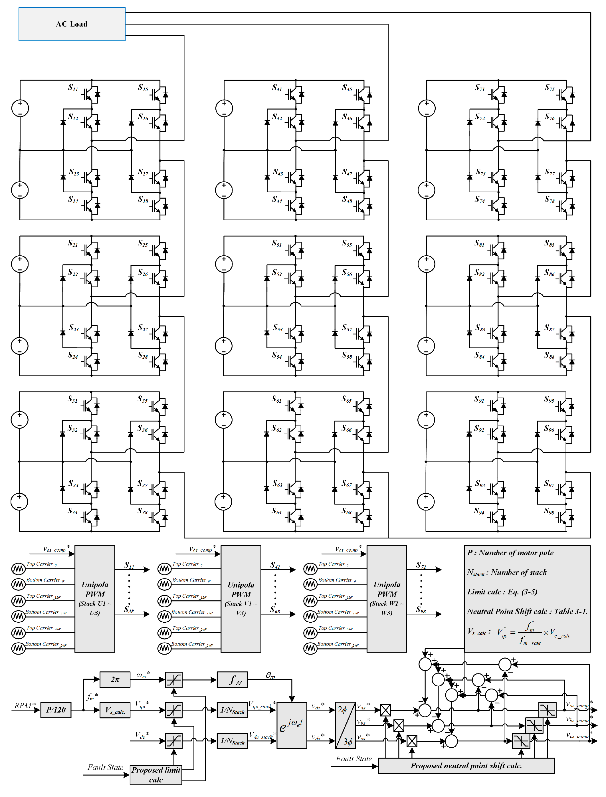
As shown in
Figure 1, the CNHB inverter requires a large number of switching devices. This growing number of switching devices increases components such as signal cables and gate units, which can eventually lead to system failures more frequently. Especially in this system, when one power stack fault occurs by components, it can potentially lead to expensive downtime. This is the biggest disadvantage of the CNHB inverter [
7,
8,
9].
To solve this problem, the CNHB inverters have a controlling method for maintaining the reduced rated voltage and power rating in order to enable continuous operation even in the case that the switching device fails in open or short circuit. The so-called “fault tolerance” for cascaded inverters has been previously investigated in the literature [
10,
11,
12,
13,
14,
15,
16].
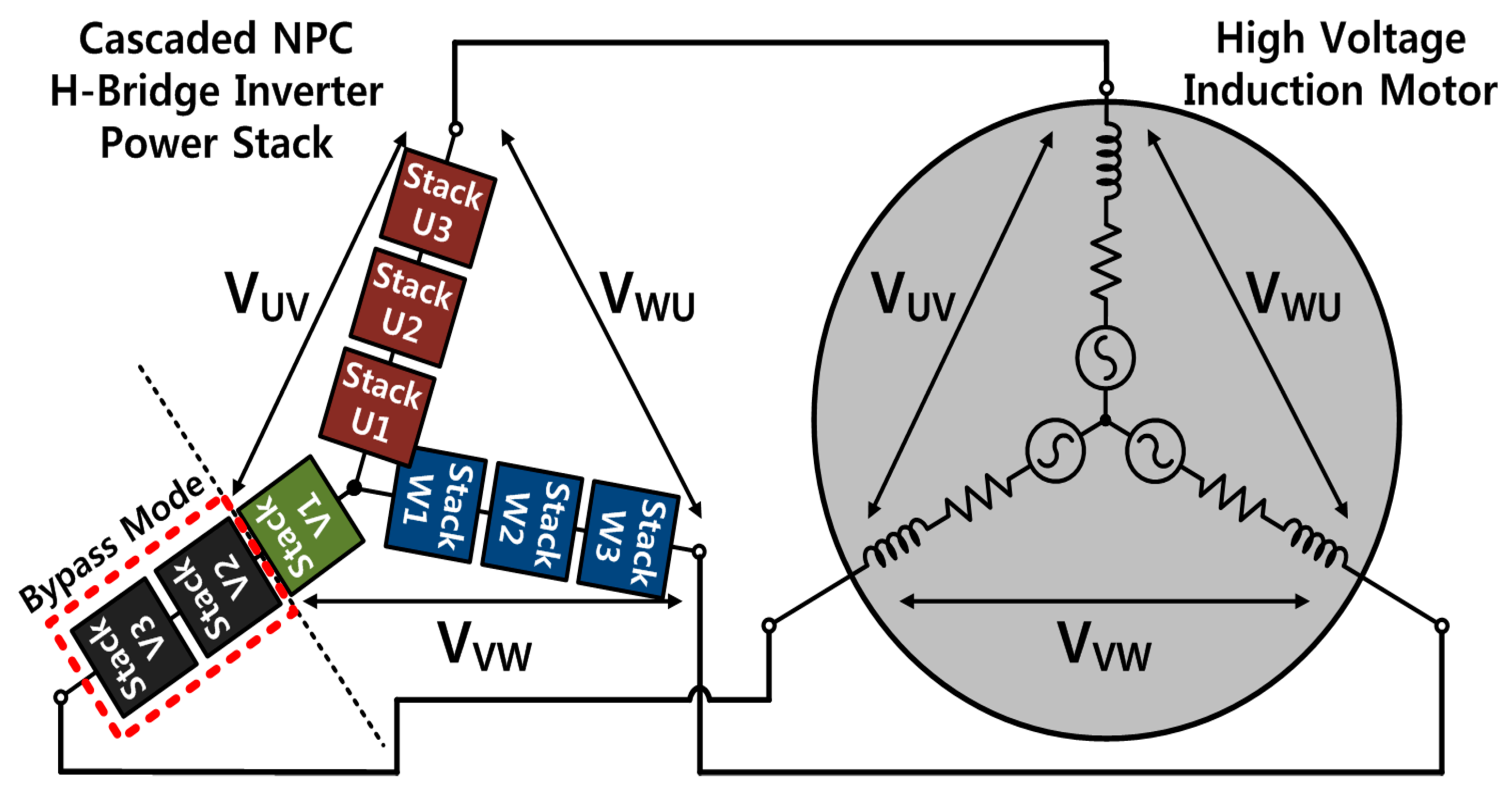
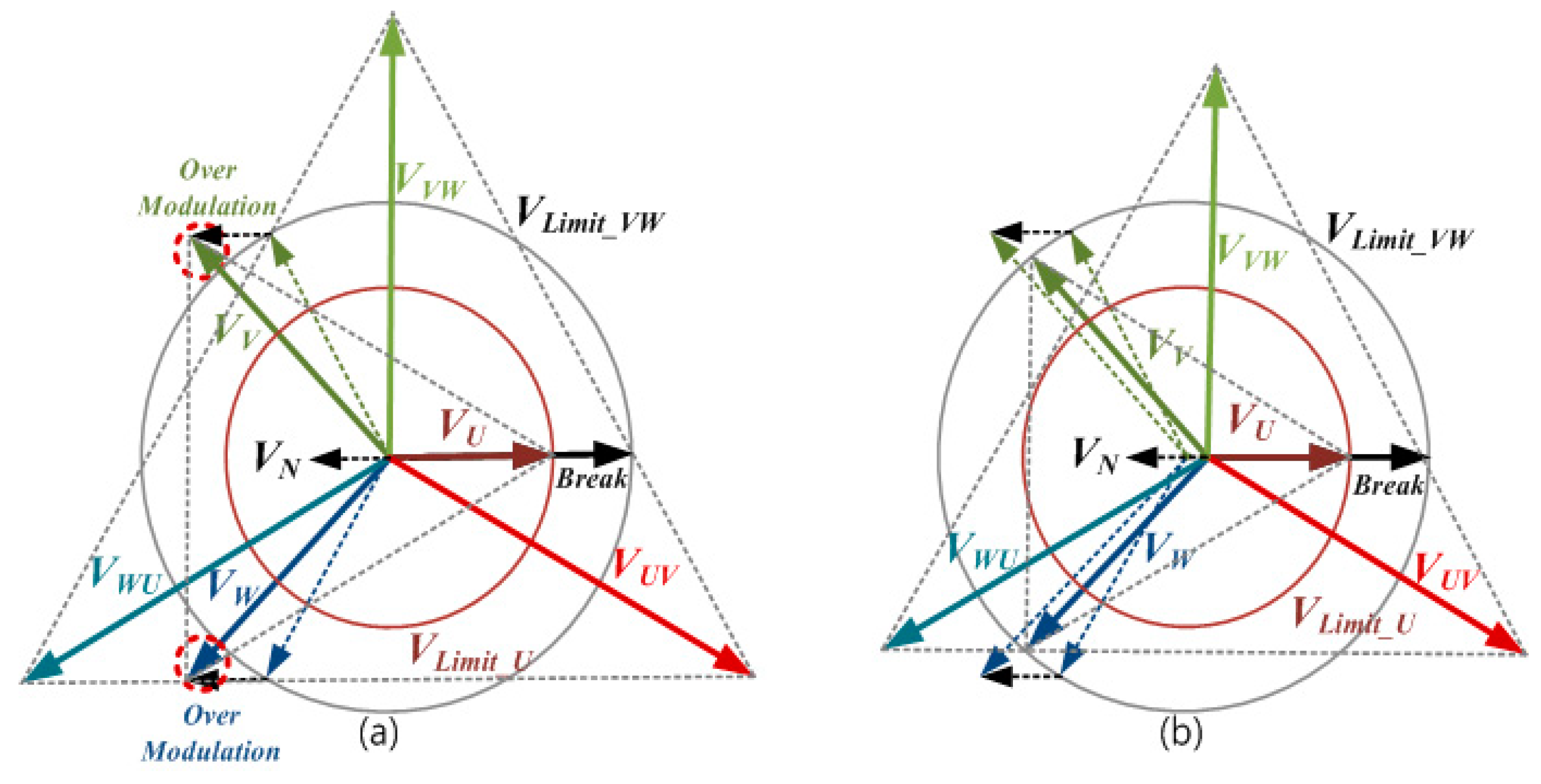
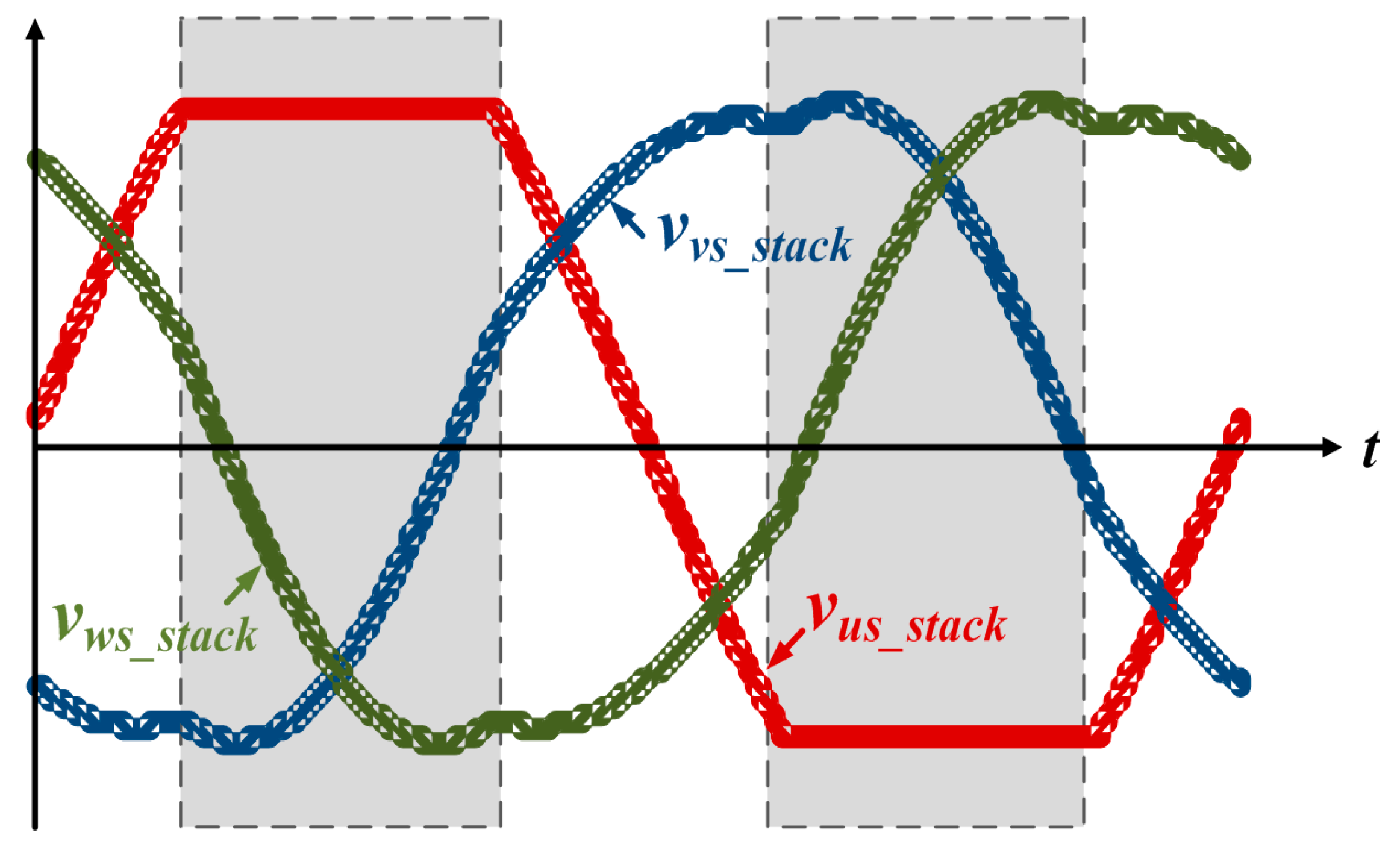
Figure 2 shows the result of applying the neutral-point voltage-shifting control, which is a conventional fault-tolerance control method. The two failed stacks are bypassed, and through fundamental-frequency zero-sequence voltage injection, the magnitude and status of the phase voltage are adjusted so that the output line-to-line voltage has a phase difference of 120 degrees [
17,
18]. This neutral-point voltage-shifting control allows the entire system to be driven without stopping. However, there arises a problem in that the available voltage range of the system is reduced and the output power is unbalanced according to the number and distribution of fault stacks. [
19,
20].
Therefore, this paper analyzes the conventional neutral-point voltage-shifting control for fault-tolerance control and proposes a novel neutral-point voltage-shifting control that can improve the individual stack output power imbalance caused by the conventional method.
This paper is organized as follows:
Section 2 analyzes the conventional fault-tolerance control for CNHB inverter;
Section 3 proposes a neutral-point voltage-shifting control that can maintain the RMS value of the output voltage of the individual stack and also describes the difference from the conventional method;
Section 4 and
Section 5 give the simulation and experimental results for the validation of the proposed control method based on the adaptive filter; and
Section 6 provides the conclusion.
3. Proposed Fault-Tolerance Control
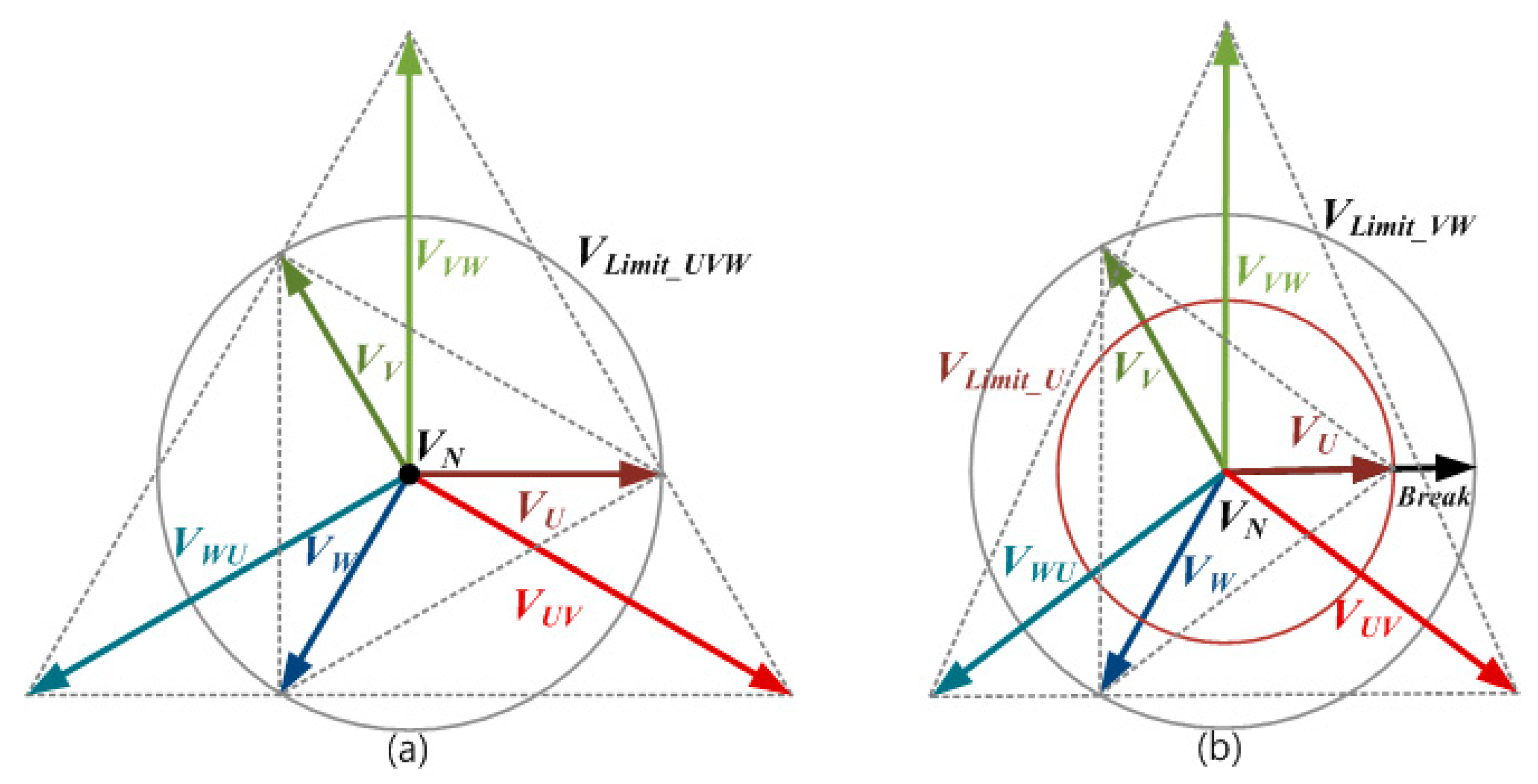
Figure 7 shows the time-dependent characteristics and the vector diagram of the proposed neutral-point voltage-shifting control. If one U phase stack fails, the phase voltage only changes in the colored area of the graph, and the phase voltage that was present in the uncolored area appears.
When the stack failure of the CNHB inverter occurs, the maximum voltage that can be modulated is lowered in the phase including the faulty stack. The proposed control does not perform the neutral-point voltage-shifting control in all of the intervals, but rather performs it only as needed according to each interval. The characteristics of the proposed control for phase voltages and line-to-line voltages to are as follows:
: The phase voltage of the phase is 0 [V], and the phases are shown as being
[V] and
[V], respectively. In this case, since there is no phase voltage of U phase, the line-to-line voltage can be expressed as Equation (14):
: In the proposed control, the phase voltage of the three-phase equilibrium is modulated up to a certain voltage in the U phase including the failed stack. In this case, the phase voltage of the phase is
[V] and the phases are shown as
[V] and
[V], respectively. The line-to-line voltage can be expressed as Equation (15):
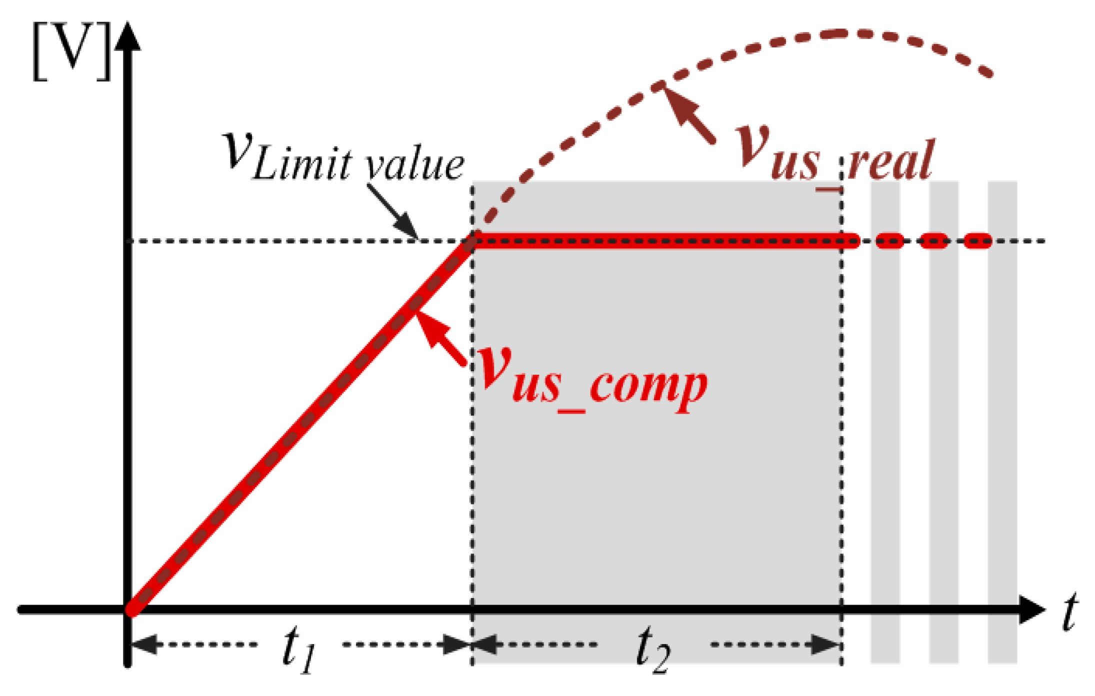
: In the proposed neutral-point voltage-shifting control, the fi is only used in the colored area. In
Figure 7, the U phase voltage is only operated up to
[V]. The voltage that should be output on U is
[V], and the insufficient voltage is about
[V]. At this time, if the voltage which is insufficient in U is modulated on the V and W phases, the V phase voltage is about
[V] and the W phase voltage is about
. The line voltage is given by Equation (16):
: The phase voltage of the U phase maintains
[V] as in
. Accordingly, the insufficient voltage is
[V], and when this voltage is compensated for, the V phase voltage and the W phase voltage are
[V] and
[V], respectively. The line voltage is given by Equation (17):
: The phase voltage of the U phase maintains
[V] as in
. Accordingly, the insufficient voltage is
[V], and when this voltage is compensated for, the V phase voltage and the W phase voltage are
[V] and
[V], respectively. The line voltage is given by Equation (18).
: Since the phase voltage of the U phase should output a voltage less than
[V] at
[V], the neutral-point voltage-shifting control is not performed. Accordingly, V phase voltage and W phase voltage are output at
[V] and
[V], respectively. Therefore, the line voltage can be expressed by Equation (19).
This proposed control uses only the neutral-point voltage-shifting control as needed for the reference voltage of the fault including the faulty stack at a voltage higher than a certain voltage, so that fault-tolerance control can be effectively performed. It is capable of randomly selecting the voltage to be maintained as shown in Equations (16)–(19). Therefore, the selected voltage compensates only for the voltage that cannot be output.
Figure 8 shows the individual stack reference voltage when one U phase stack fails. Because one stack is broken, only the remaining two stacks are used to produce the same output voltage as the three stacks. Therefore, multiplying the ratio of 1.5 by the reference voltage increases the reference voltage
of the two stacks. Therefore, when the maximum and minimum values are selected for the increased reference voltage, the U phase individual stack reference voltage is generated, as shown in the red line in
Figure 8. At this point, if the difference between the previous value and the subsequent value is subtracted from the V phase and the W phase, separate stack reference voltages, like the green line and blue line in
Figure 8, are generated. In this paper, the criteria for selecting the maximum and minimum values for the proposed neutral-point voltage-shifting control is selected as the limit value at which the RMS value of the output phase voltage of the individual stack becomes equal. This control method that is proposed enables the same output power for each stack.
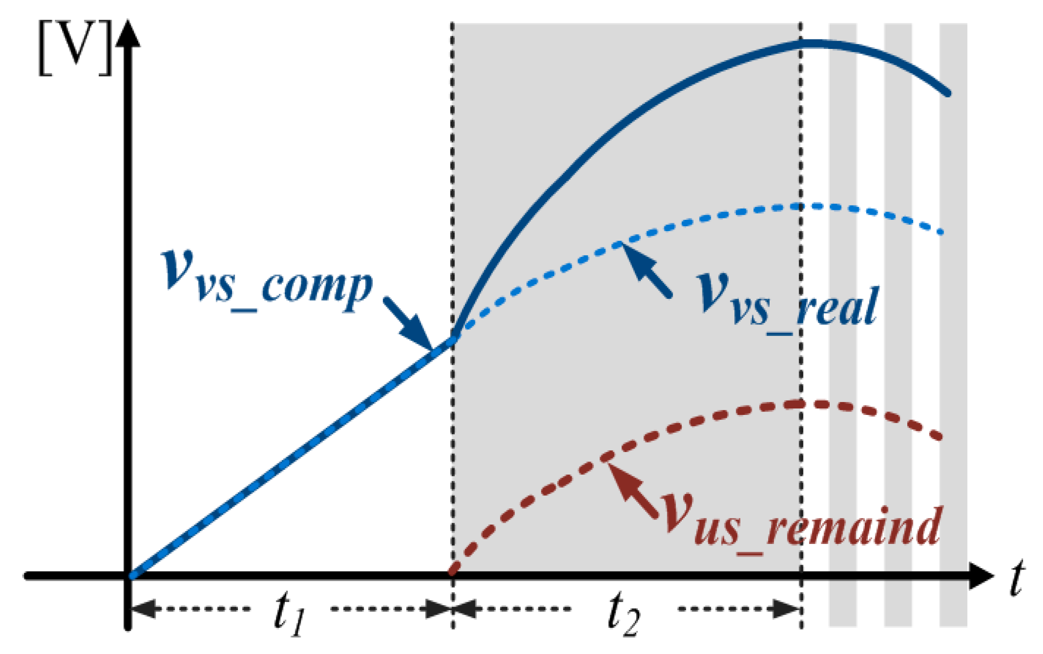
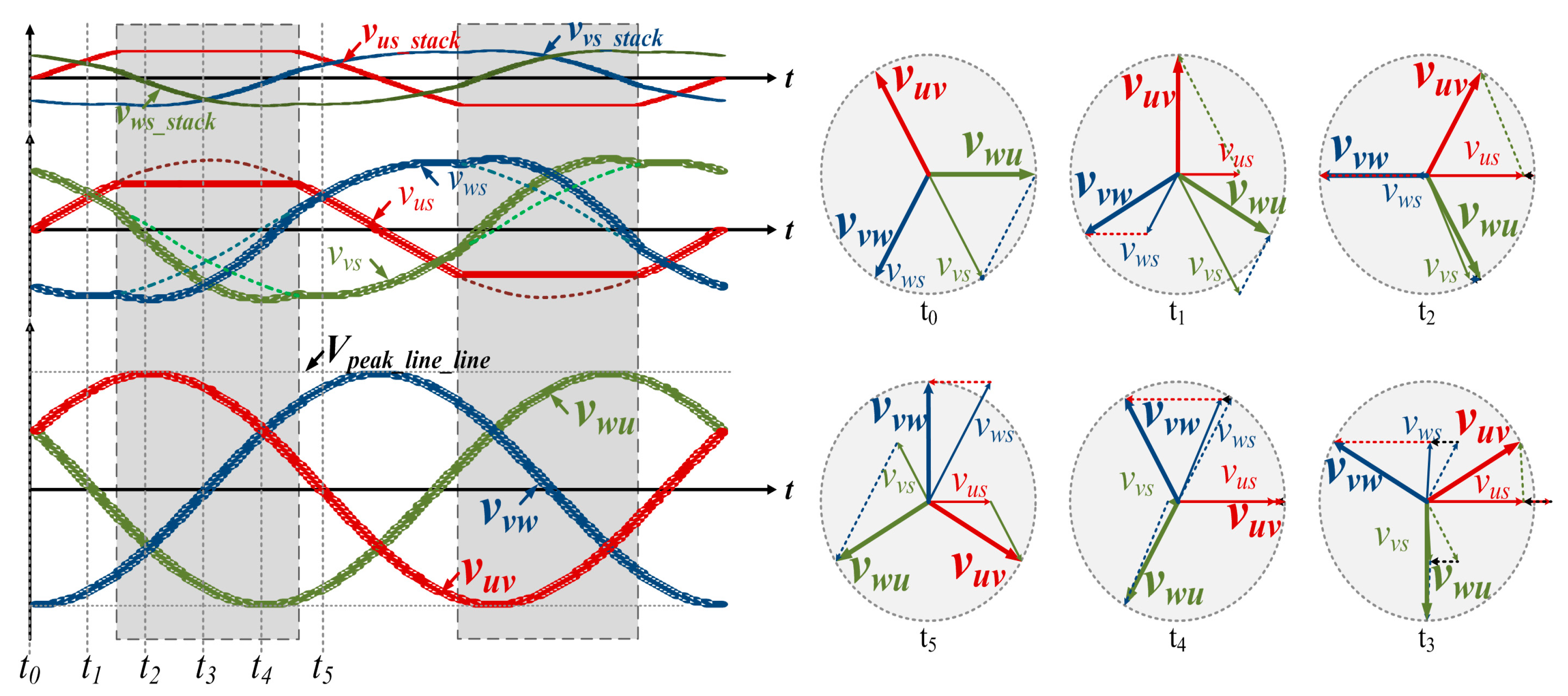
Figure 9 shows a quarter period waveform of each stack reference voltage when the proposed neutral-point voltage-shifting control is used for U phase failure.
is the reference voltage before limit and
is the reference voltage after limit. In this paper, in order to calculate the RMS value of the proposed reference voltage, the reference voltage on the non-sinusoidal periodic U is constructed as a primitive function. Then, the RMS values at
and
with respect to the 1/4 periodic wave are respectively calculated and added.
To calculate the RMS value, a calculation for
t1 is necessary. Since
and
are the same during
, they can be expressed as Equation (20).
The time
at which the reference voltage reaches the maximum value can be expressed by Equation (21) using Equation (20).
Through Equation (21), the RMS value of the reference voltage during the period
can be expressed as Equation (22).
The time
can be expressed as Equation (23), and the RMS value can be expressed as Equation (24).
Figure 10 shows a quarter period waveform of V phase stack reference voltage when using the proposed neutral-point voltage-shifting control for U phase failure.
is the value obtained by subtracting
from
in
Figure 10. In order to calculate the RMS value of the V phase reference voltage, the reference voltage on the non-sinusoidal phase V is constructed as a base function, and then the RMS value of
and the RMS value of
are calculated.
The quarter-period RMS value for
is given by Equation (25).
The RMS value for
can be expressed by Equation (26) using Equations (24) and (25).
The proposed control assigns
so that the value obtained by adding the RMS values of Equations (22) and (24) is equal to the sum of Equations (25) and (26). This can be expressed as Equation (27).
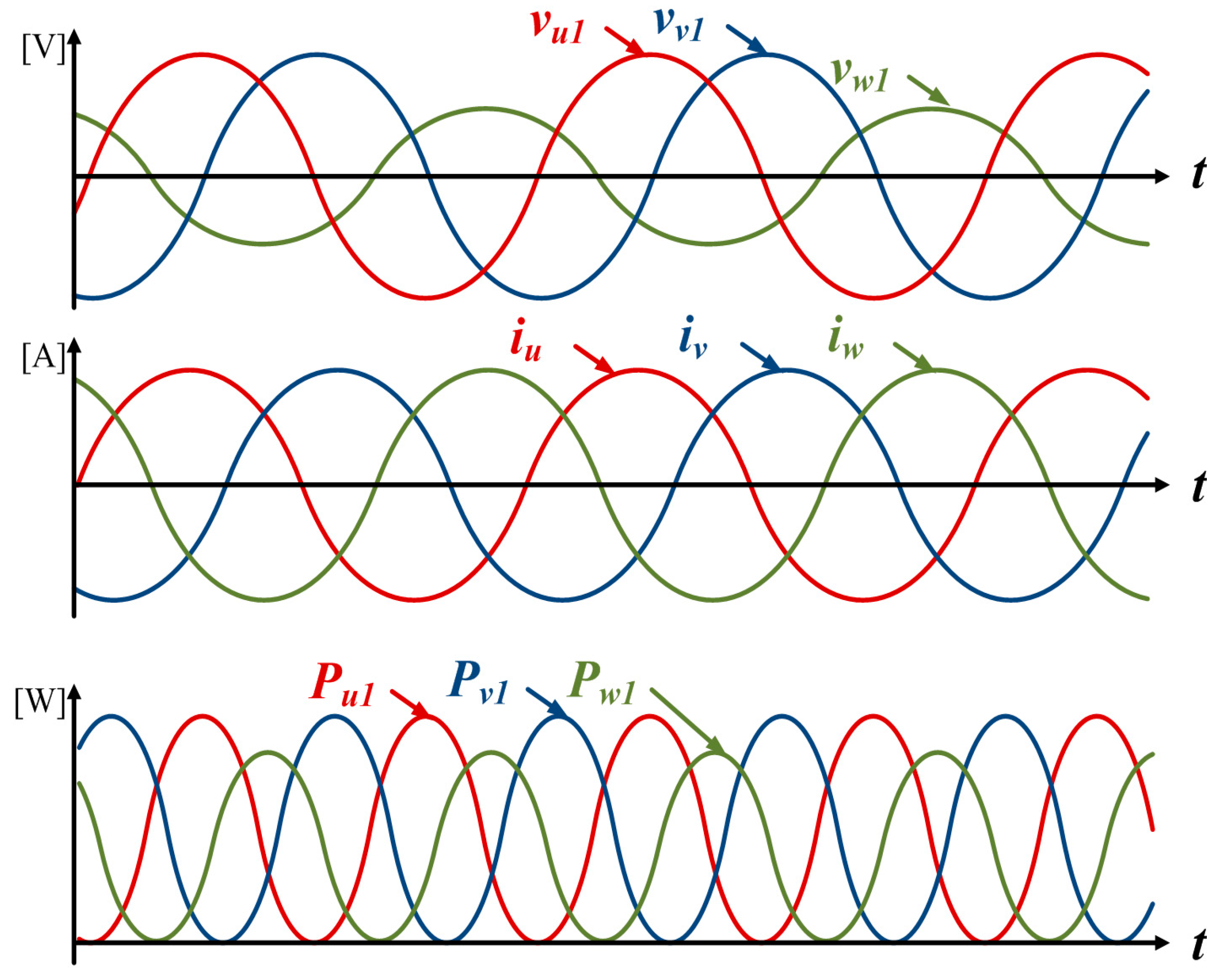
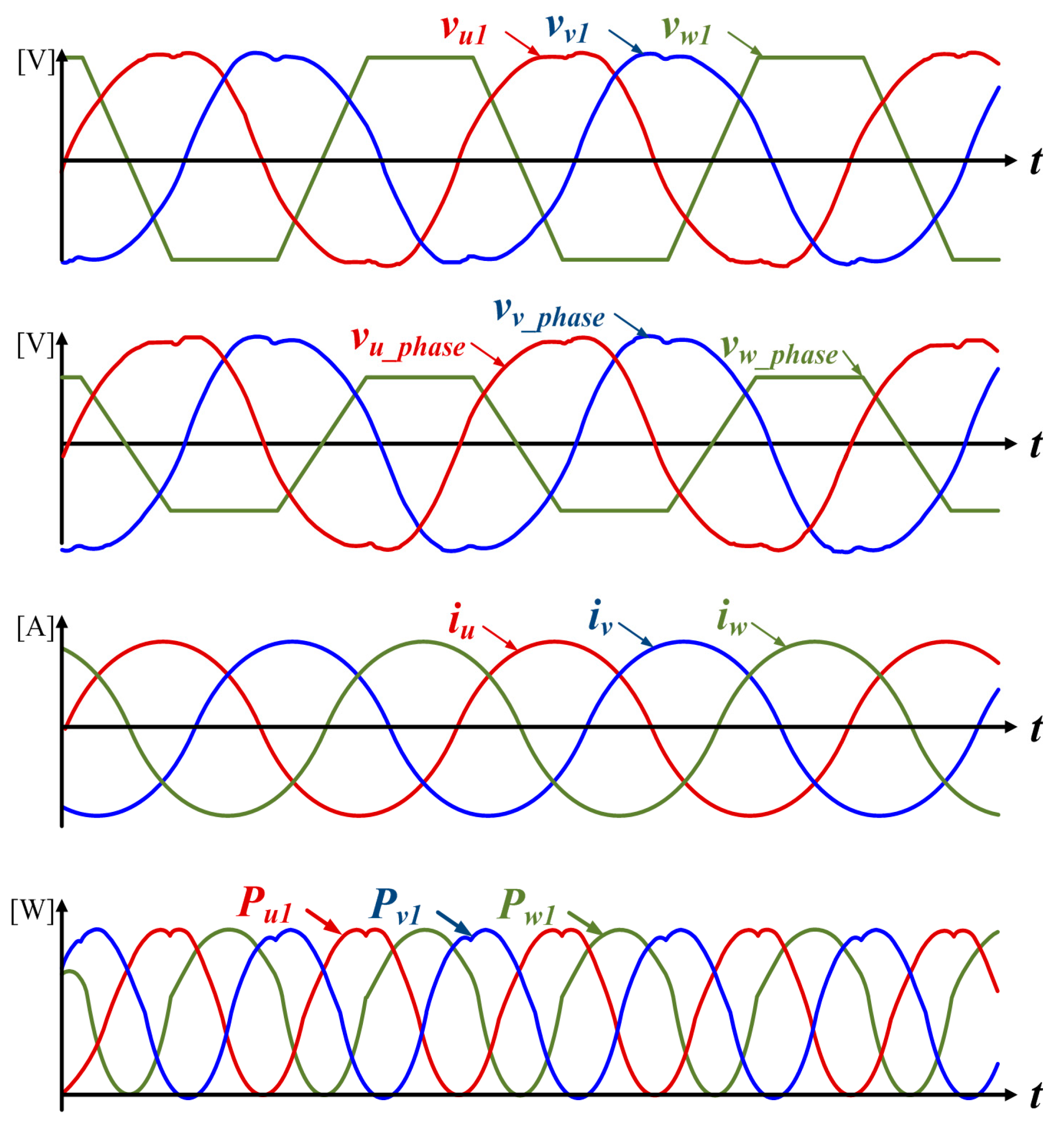
Figure 11 shows the waveforms of the individual stack voltage waveforms, the phase voltage, the phase current, and the stack power in the proposed neutral-point voltage-shifting control. As shown in
Figure 11, if the RMS value of each stack reference voltage is kept the same, the average value of output power of each stack can be the same. Therefore, even if the stack fails, the line-to-line voltage maintains three-phase equilibrium, and the output power imbalance, which is a disadvantage of the conventional neutral-point voltage-shifting control, can be improved.
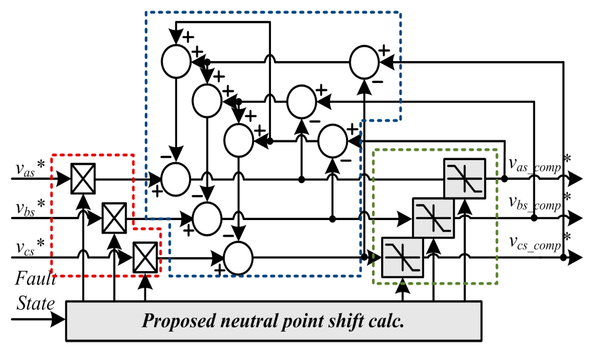
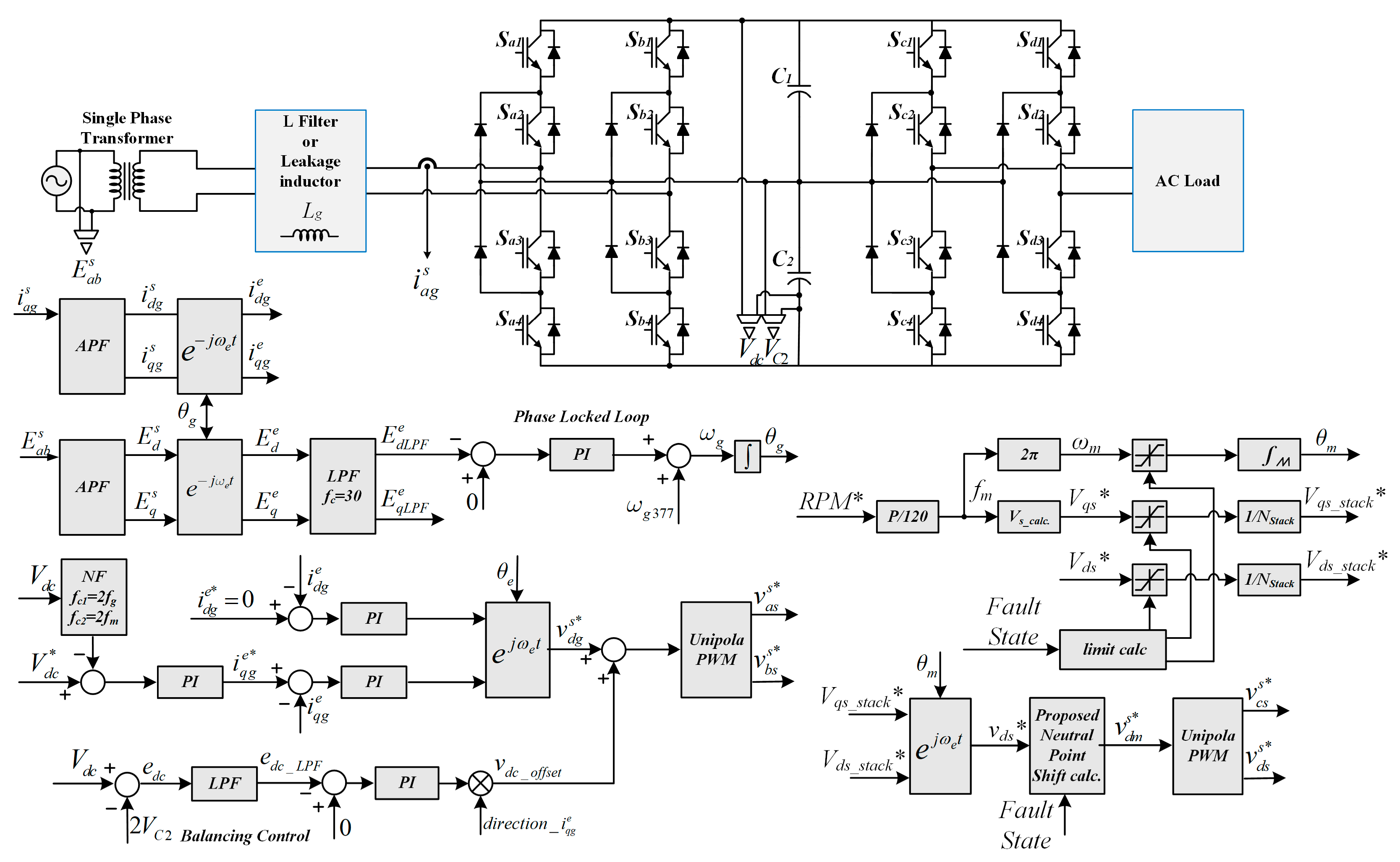
Figure 12 shows a block diagram of the proposed fault-tolerance control. The proposed control consists of three major parts: the part that varies the reference of the phase voltage and the reference voltage limiter, the part that subtracts the difference between the previous value and the subsequent value of each phase from the other phase reference voltage, and the part that calculates the maximum and minimum values of the reference voltage and limiter for the neutral-point voltage-shifting control.
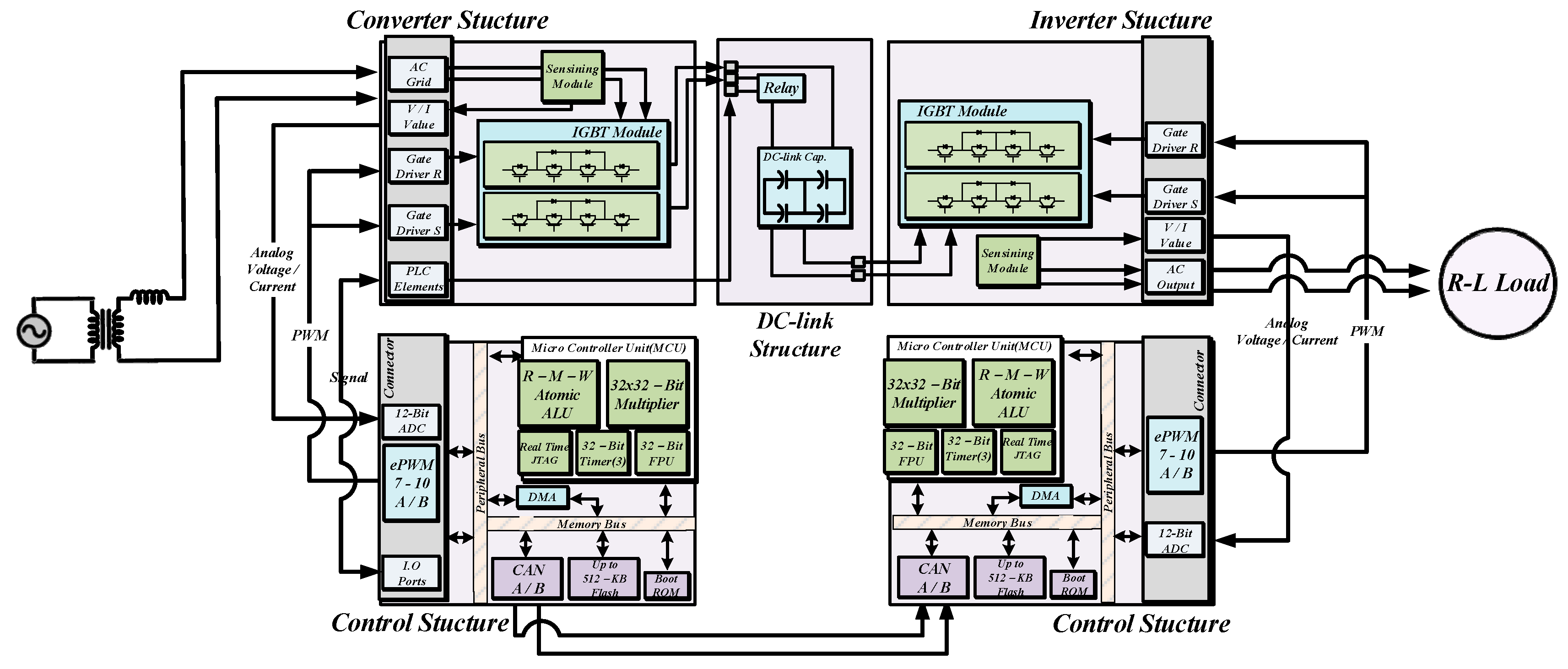
Figure 13 shows a schematic configuration and a control block diagram of a single cascaded NPC/H-bridge system using the proposed neutral-point voltage-shifting control. As shown in
Figure 13, the system dealt with in this paper consists of NPC/H-bridge inverter and NPC/H-bridge converter in back to back. The NPC/H-bridge converter performs grid power factor control, DC-link voltage control, and DC-link neutral-point voltage-balancing control. In this case, the DC-link is represented by an equivalent circuit and the control block diagram of the 13-level cascaded NPC/H-bridge inverter is shown in
Figure 14.
As shown in
Figure 14, the proposed neutral-point voltage-shifting control is applied based on the V/F control method, and the maximum voltage and the maximum speed according to the fault state are set in the same condition as the conventional method.
4. Simulation Results
In order to verify the principle and feasibility of the proposed control method, a simulation has been developed using the PSIM software program. The simulation schematic in the 13-level cascaded NPC/H-bridge system is illustrated in
Figure 1. The systems parameters of the simulation and experiment are shown in
Table 1.
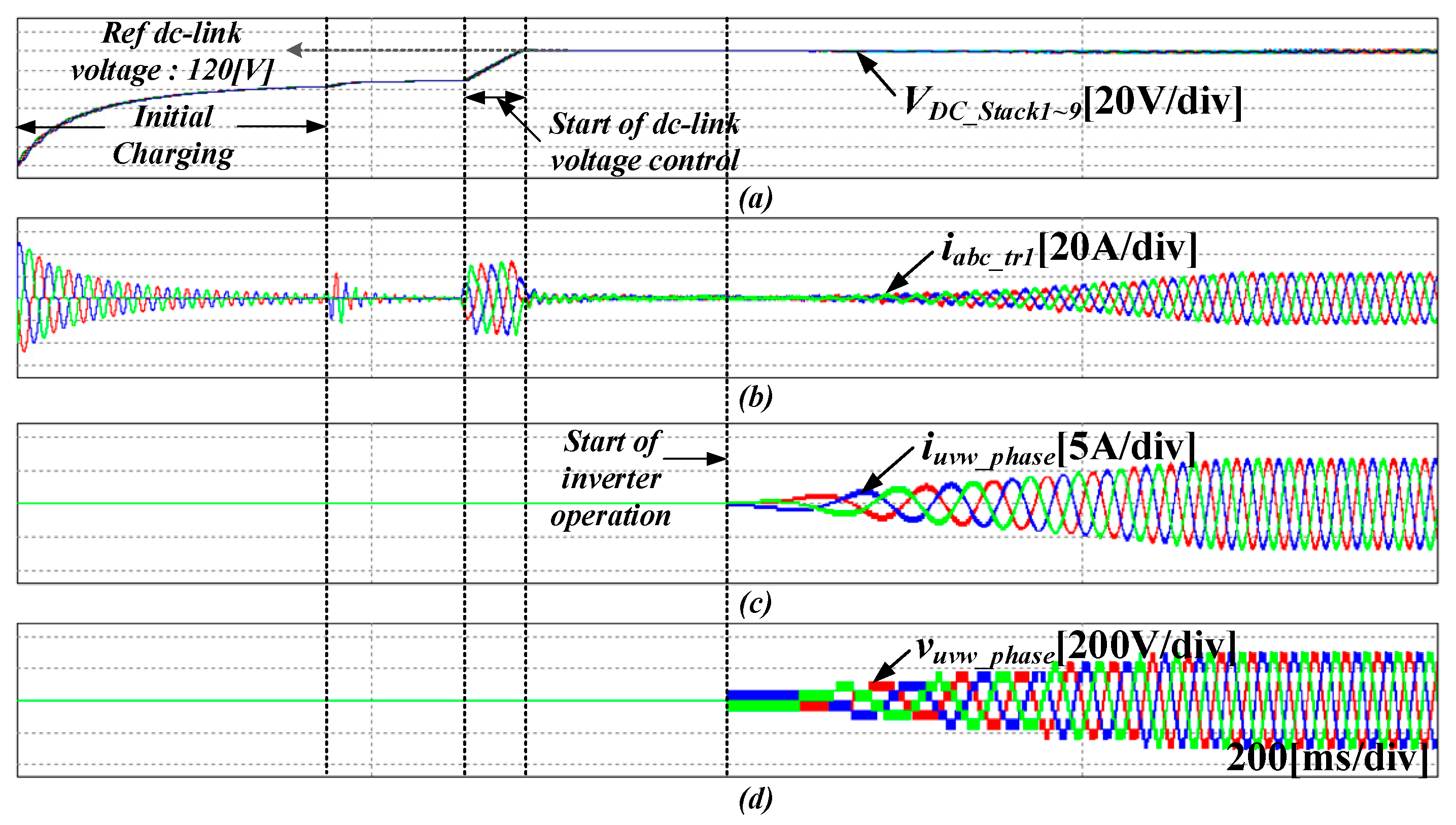
Figure 15 shows the operating waveform of the 13-level NPC/H-bridge converter and inverter. As shown in
Figure 15, the converter was operated at first to control the DC-link voltage. Then the inverter reached the steady state and the inverter was operated.
Figure 16 shows the simulation result of the NPC/H-bridge converter applying the neutral-point voltage-balancing control of the DC-link mentioned in
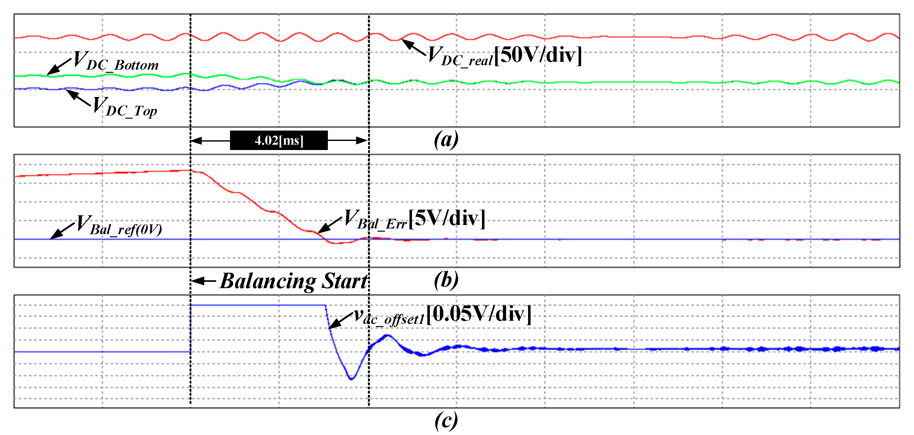
Figure 13. In the process of operating the 13-level NPC/H-bridge inverter, when imbalance occurs in the neutral voltage of the DC-link due to stack faults or sudden load change, it affects the output current of the inverter. Therefore, the neutral-point voltage balancing of the DC-link is continuously performed in the NPC/H-bridge converter. The simulations artificially applied an unbalanced load to the DC-link to verify the neutral-point voltage-balancing control and performed the balancing control at a certain point in time. As can be seen from the waveform of the simulation, the DC-link voltage-balancing control is performed stably even if the voltage of the top and bottom capacitors is unbalanced.
Figure 17 shows the simulation waveform for the failure of the V phase fourth stack of the 13-level NPC/H-bridge inverter. The waveforms are, in order, individual stack reference voltage on U, V, W, output voltage of the first to ninth stack, voltage on U, V, W; line-to-line voltage of UV, VW, WU; phase voltage of U, V, W; and phase current.
When operating with a reference voltage of three-phase equilibrium when a stack fault occurs as shown in
Figure 17, the phase voltage of the phase including the fault stack, as the V phase voltage, is reduced and the three-phase equilibrium of the phase current is not made. Therefore, it is necessary to maintain the three-phase equilibrium of the line voltage using the neutral-point voltage-shifting control.
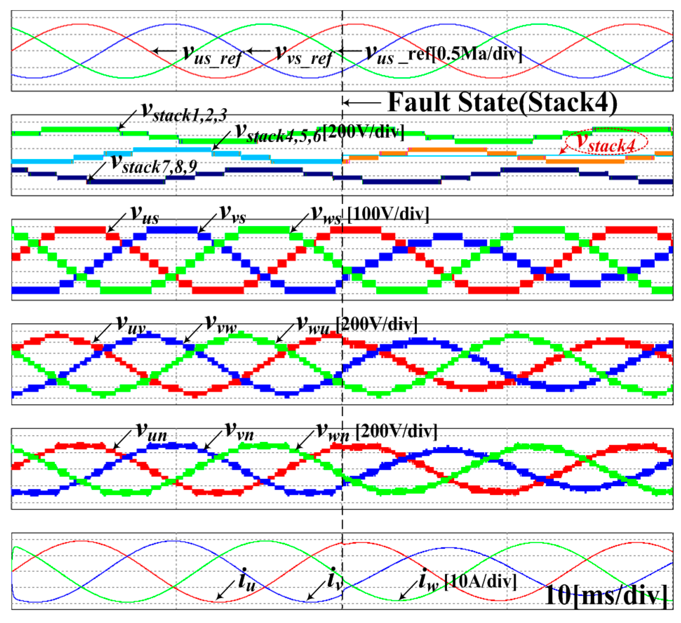
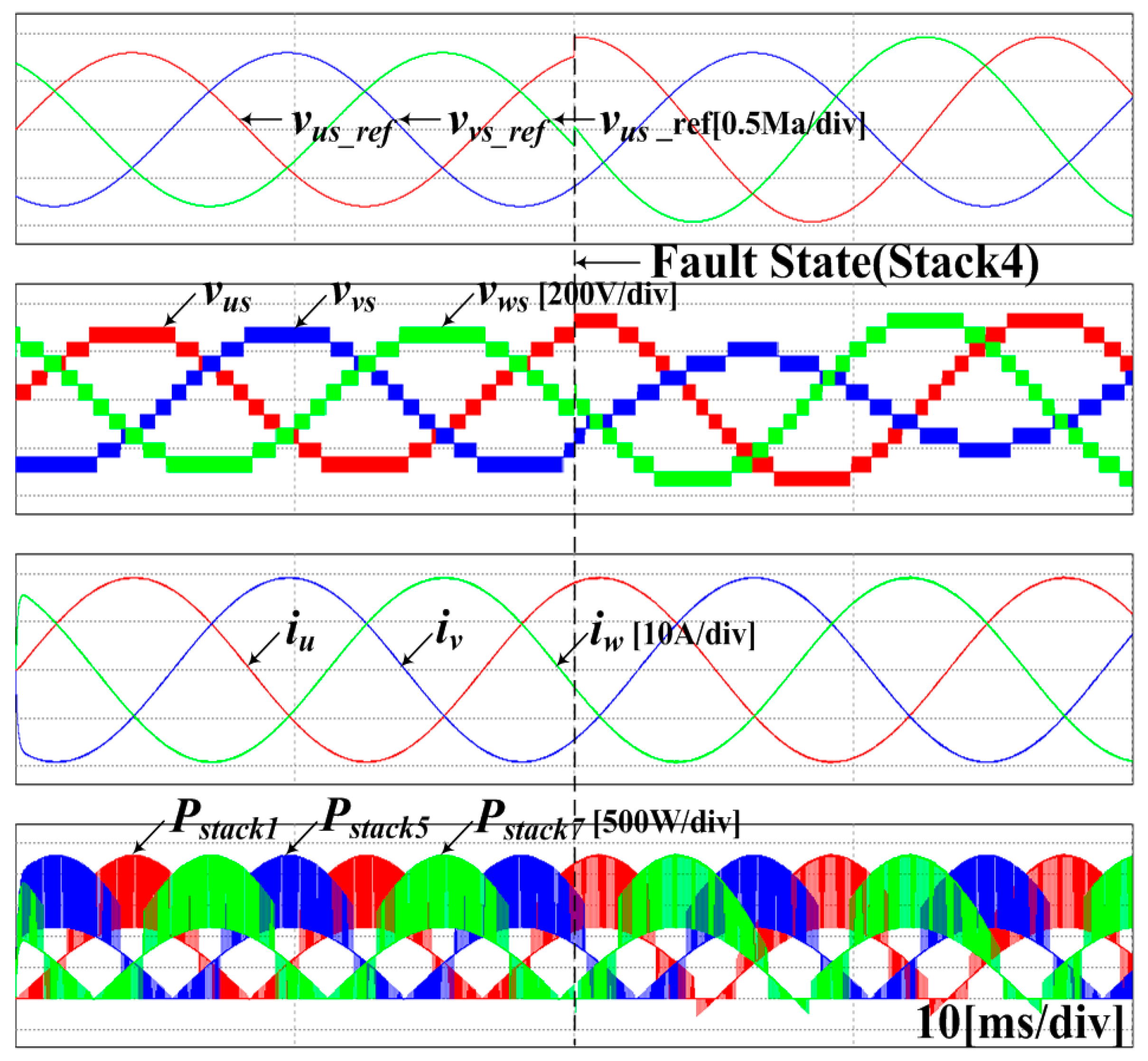
Figure 18 shows simulation waveform when V phase fourth stack fails in applying the conventional neutral-point voltage-shifting control. The order of the waveforms is the same as in
Figure 17. In case of fault, the phase voltages of the U and W phases are larger than that of the V phase, but the line-to-line voltage for UV, VW, and WU is shown as three-phase equilibrium. This results in a three-phase equilibrium between the load voltage. The load current will also have three-phase equilibrium flowing through it.
However, when using the conventional neutral-point voltage-shifting control, an output power imbalance occurs between the individual stacks, as shown in
Figure 19. The RMS values of the average power and reference voltage are summarized in
Table 2 when using the conventional neutral-point voltage-shifting control shown in
Figure 19.
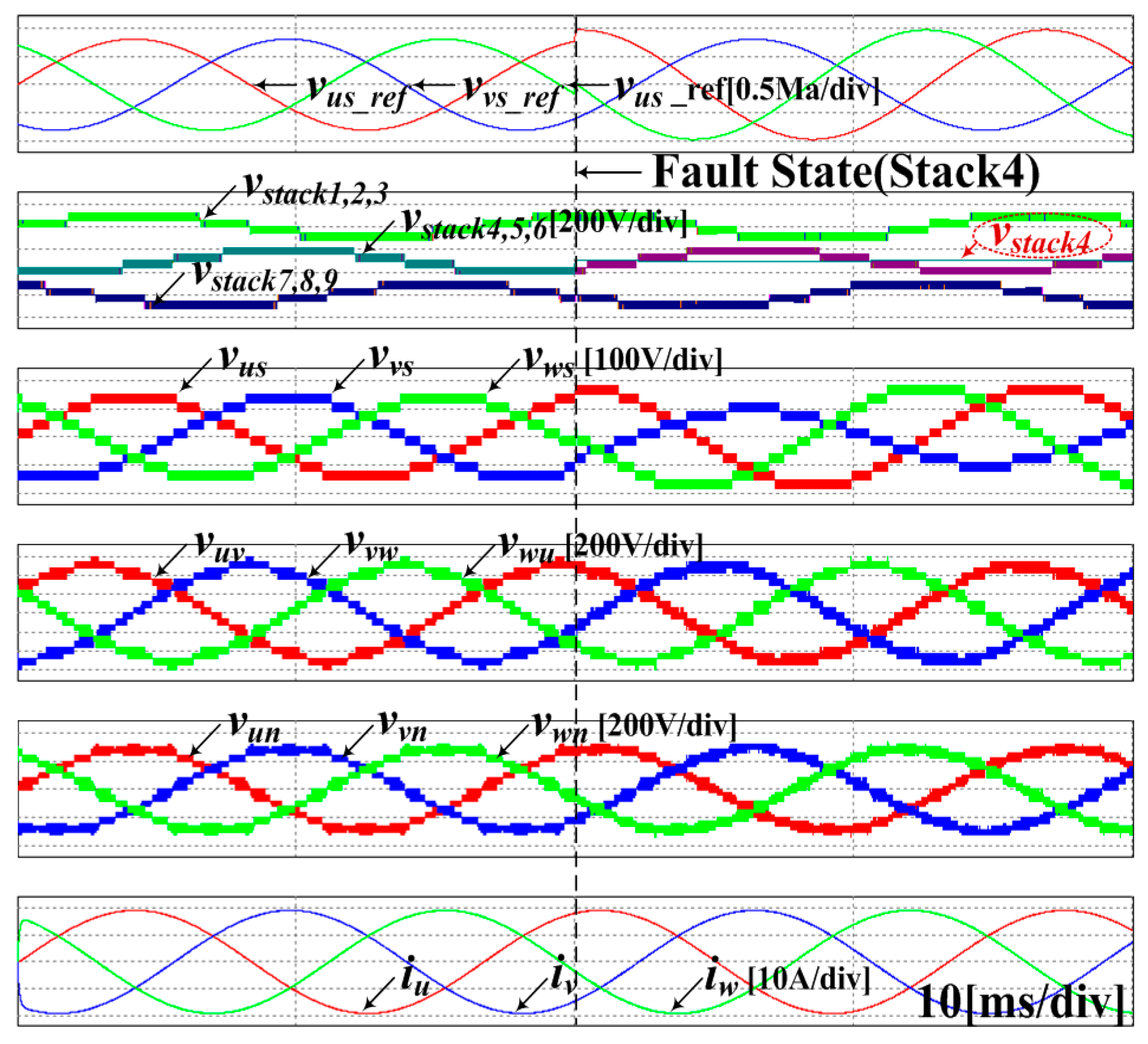
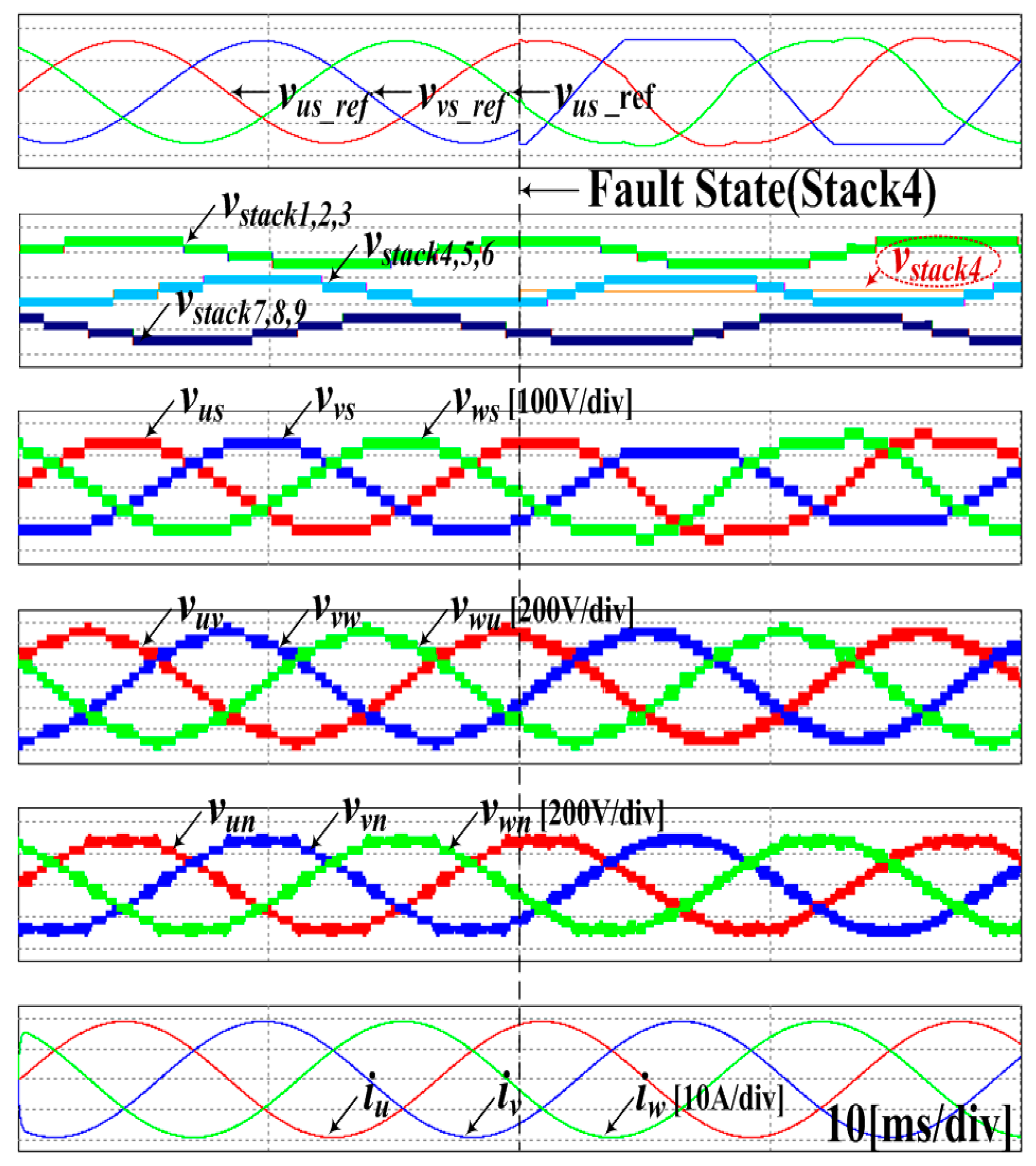
Figure 20 shows the simulation waveform of the proposed neutral-point voltage-shifting control for V phase fourth stack failure. The order of the simulation waveform is the same as those in
Figure 17 and
Figure 18. In the case of the proposed control, the reference voltage for the neutral-point voltage-shifting control is formed while the RMS value of the reference voltage is kept the same.
Figure 21 shows the simulation waveform including the individual stack power when using the proposed neutral-point voltage-shifting control. In the proposed control, the faulty stack increases the Ma value to increase the RMS value, and there is a section that maintains the DC type reference voltage like the blue line of the first waveform in
Figure 21 while passing through the limit function. The reference voltage and the phase voltage are modulated while the U and W phase reference voltages perform the neutral-point voltage-shifting control by this interval.
As a result of the selective neutral-point voltage-shifting control, the three-phase balance of the load current is maintained, and the RMS values of the average output power and the reference voltage are shown in
Table 3. In addition, the phase current THD of the proposed method is compared with that of the conventional method, as shown in
Table 4.
5. Experiment Results
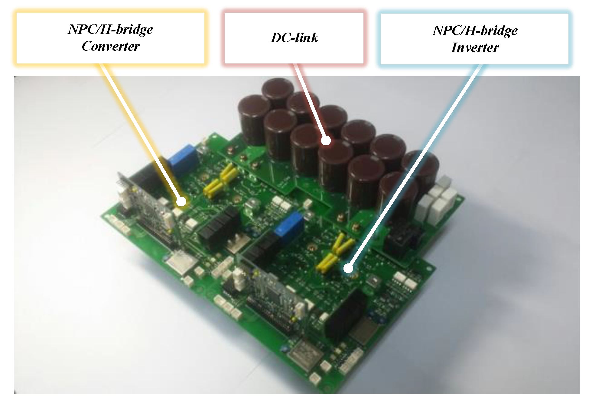
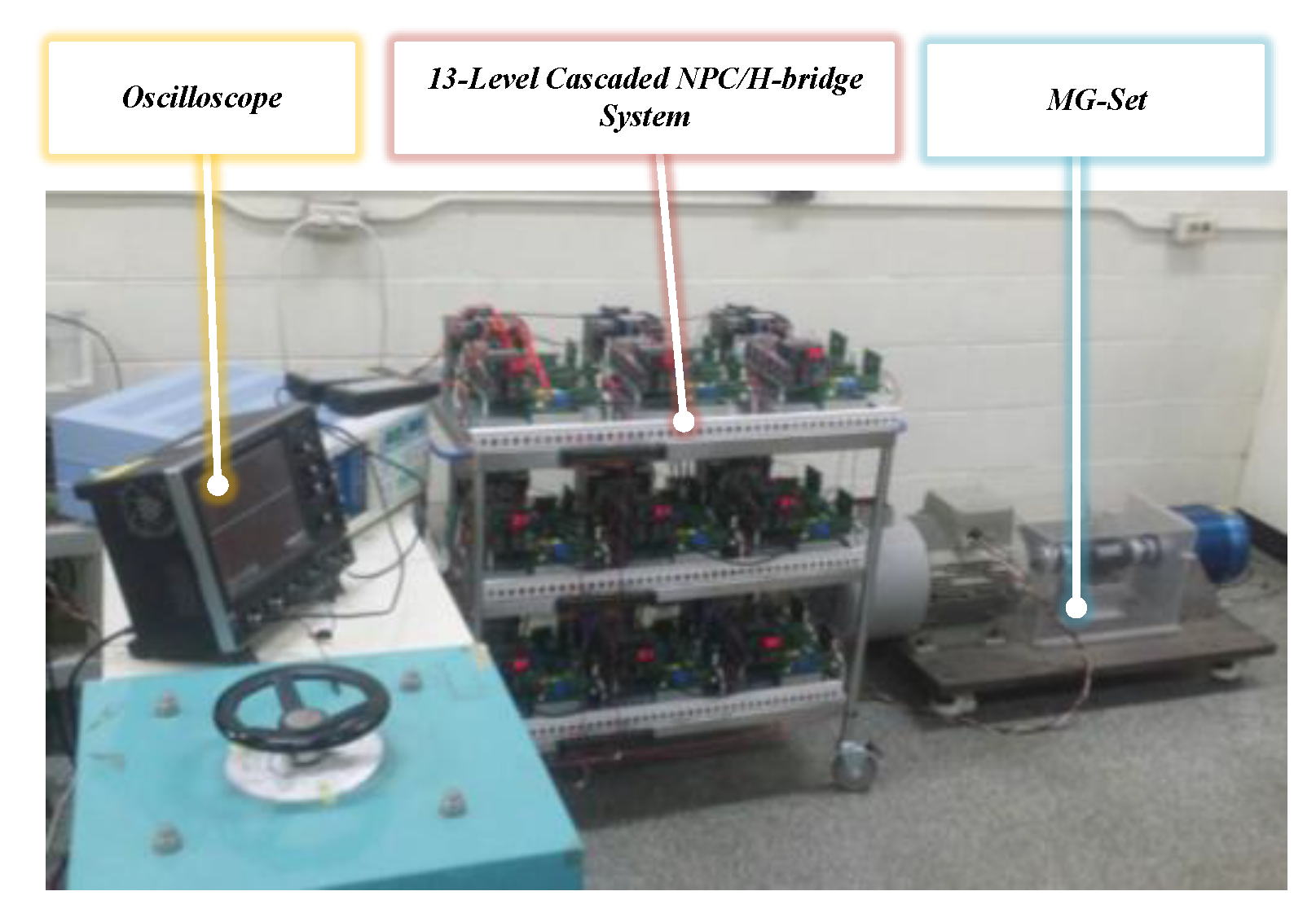
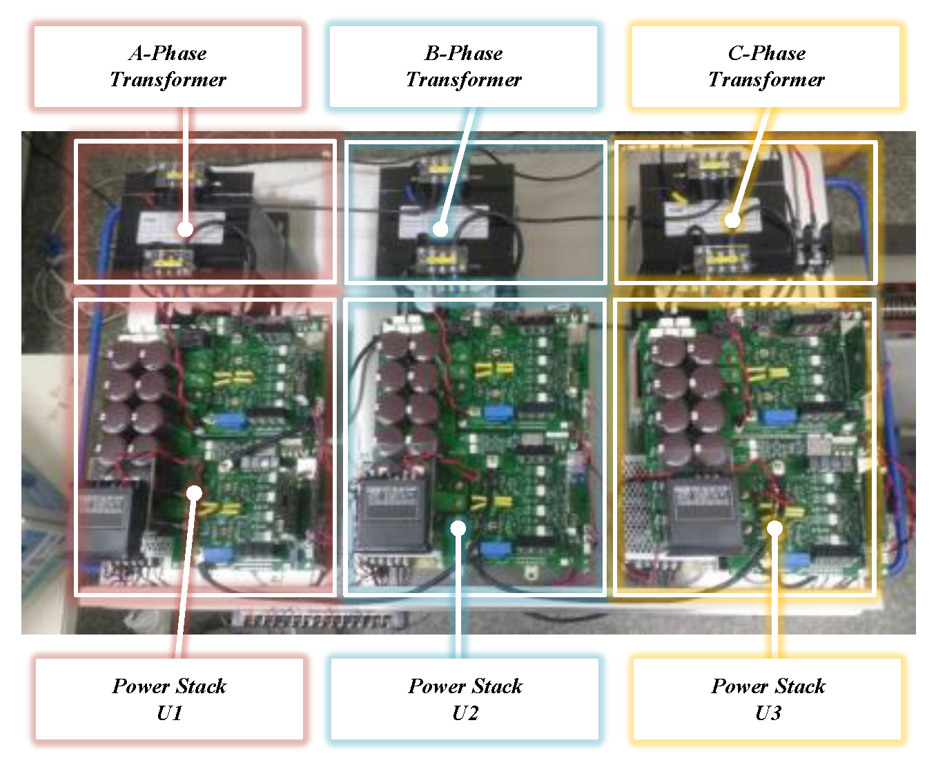
An experiment was performed to verify the feasibility of the proposed control method applied in a cascaded NPC/H-bridge inverter. The configurations of the experimental system and power stacks were as shown in
Figure 22,
Figure 23,
Figure 24 and
Figure 25, and the experimental parameters as in
Table 1.
The controller was implemented on TMS320F28377s, and that of the floating point microcontroller unit at 200 MHz rate frequency. The switching and sampling frequency was 10 kHz. The power was supplied to the cascaded NPC/H-bridge inverter through the cascaded NPC/H-bridge converter.
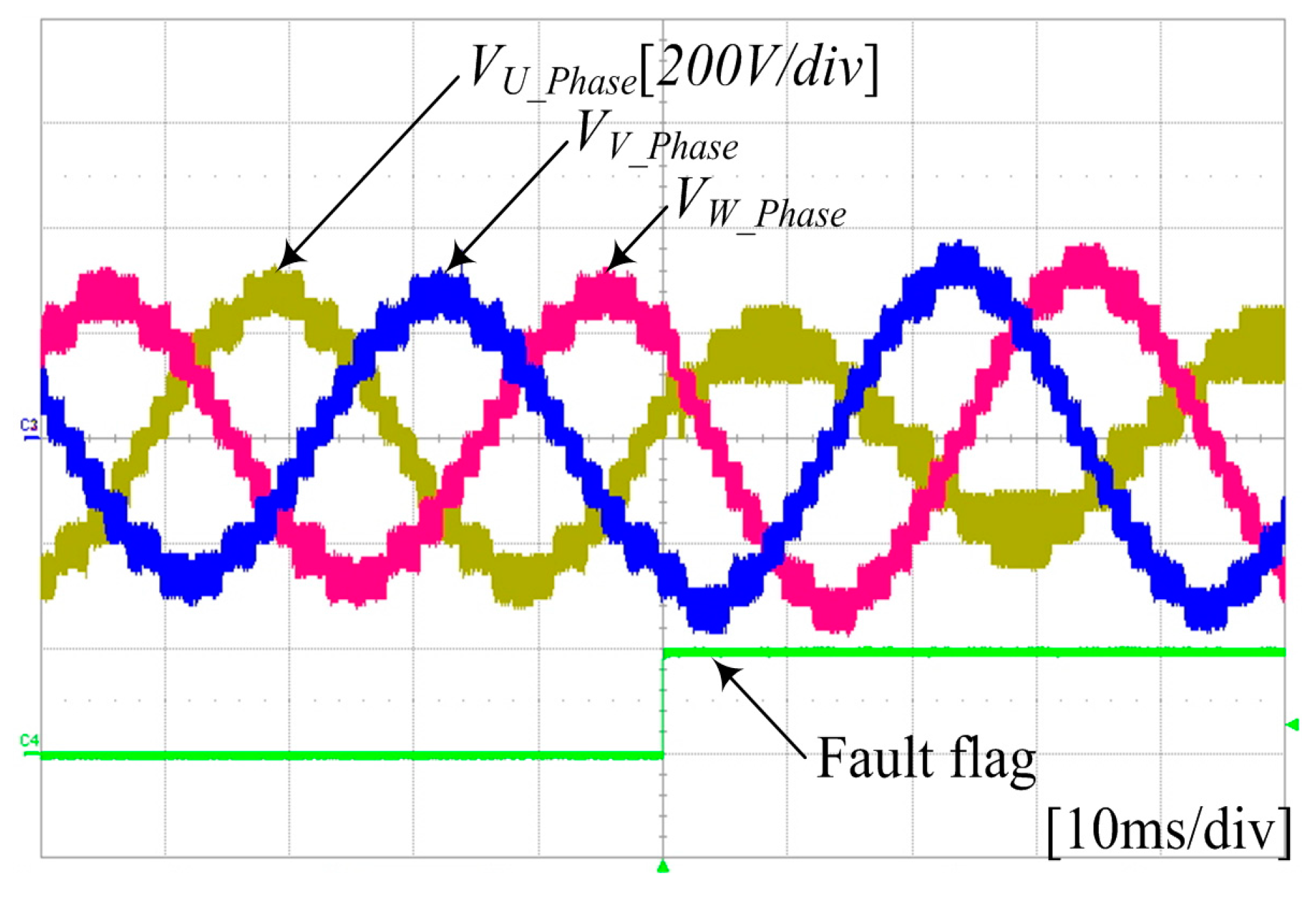
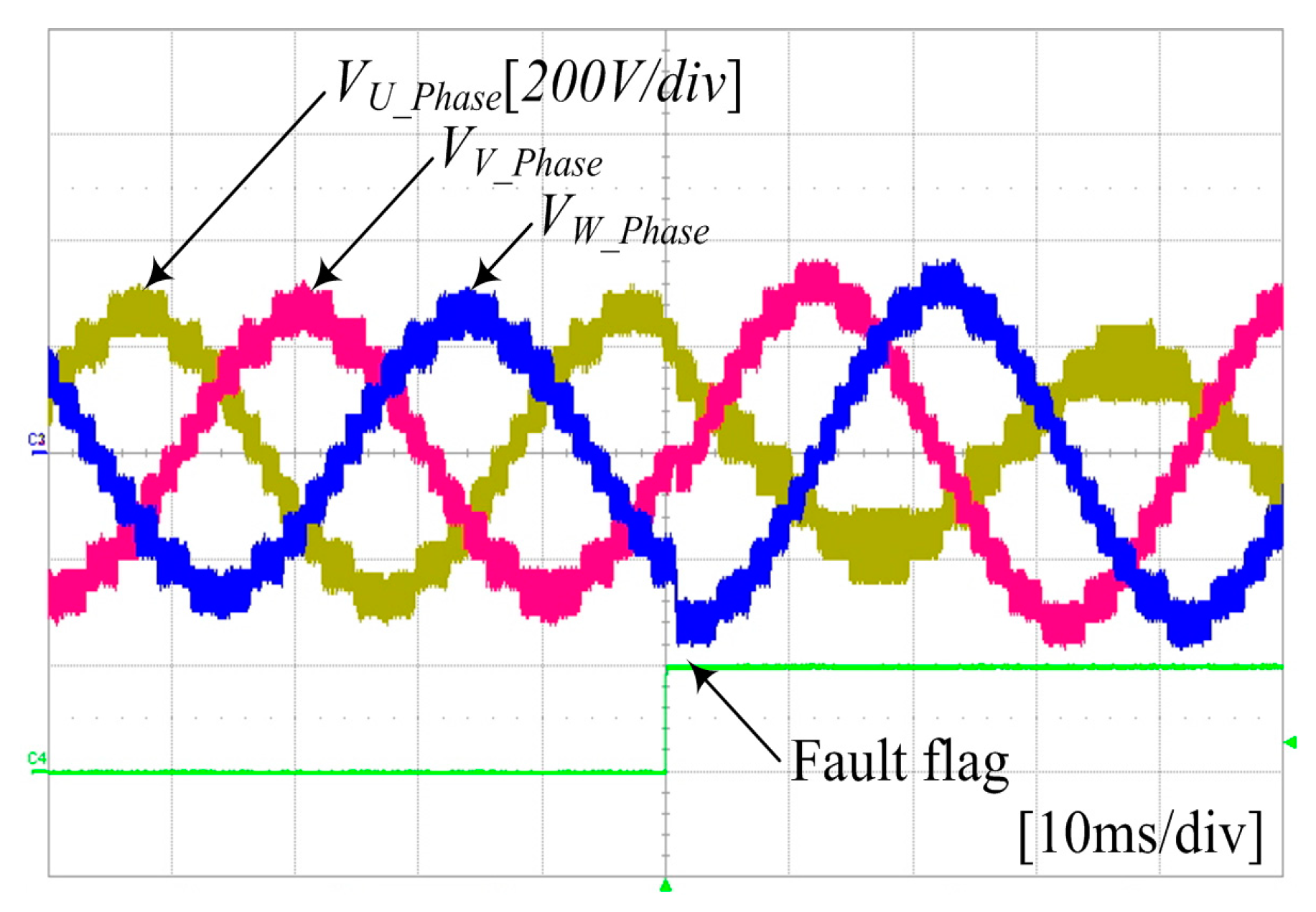
Figure 26 shows the waveform of the phase voltage of each phase when applying the conventional neutral-point voltage-shifting control. The experiment involves an experimental waveform for the individual phase voltage and fault flags for any faults during inverter operation. Fault is generated in the first stack of the U phase, so that the voltage of the U phase is lowered and the output voltages of the V and W phases are increased.
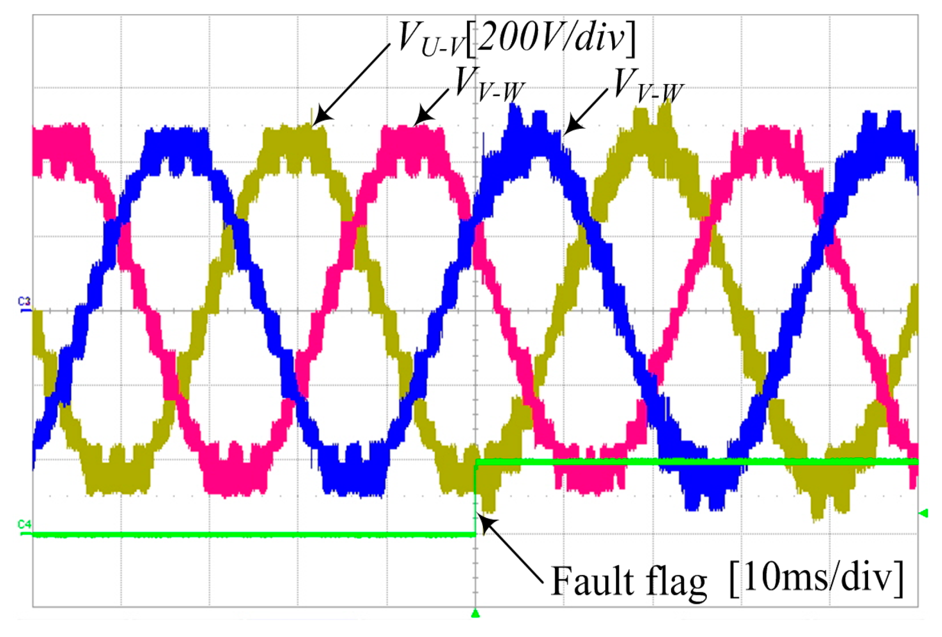
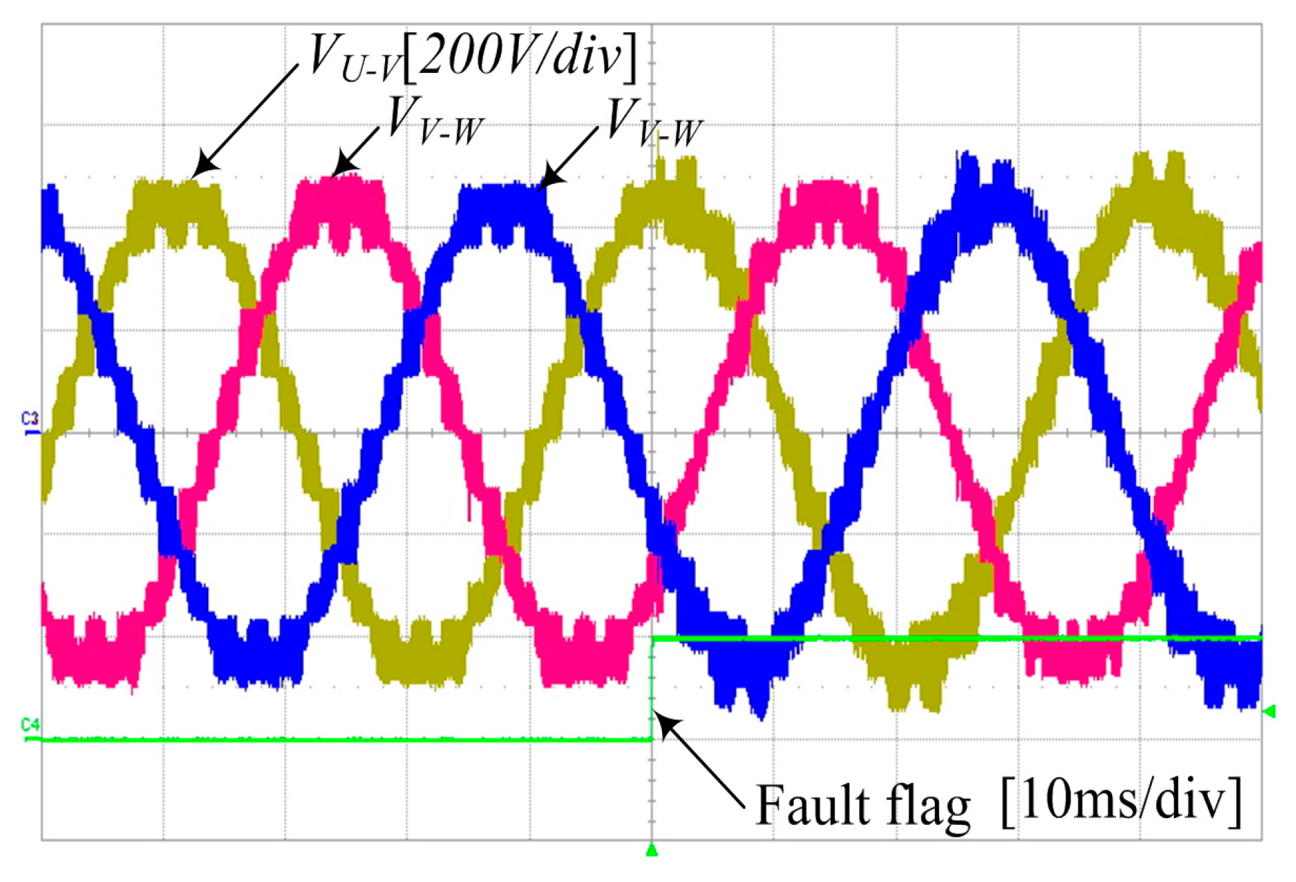
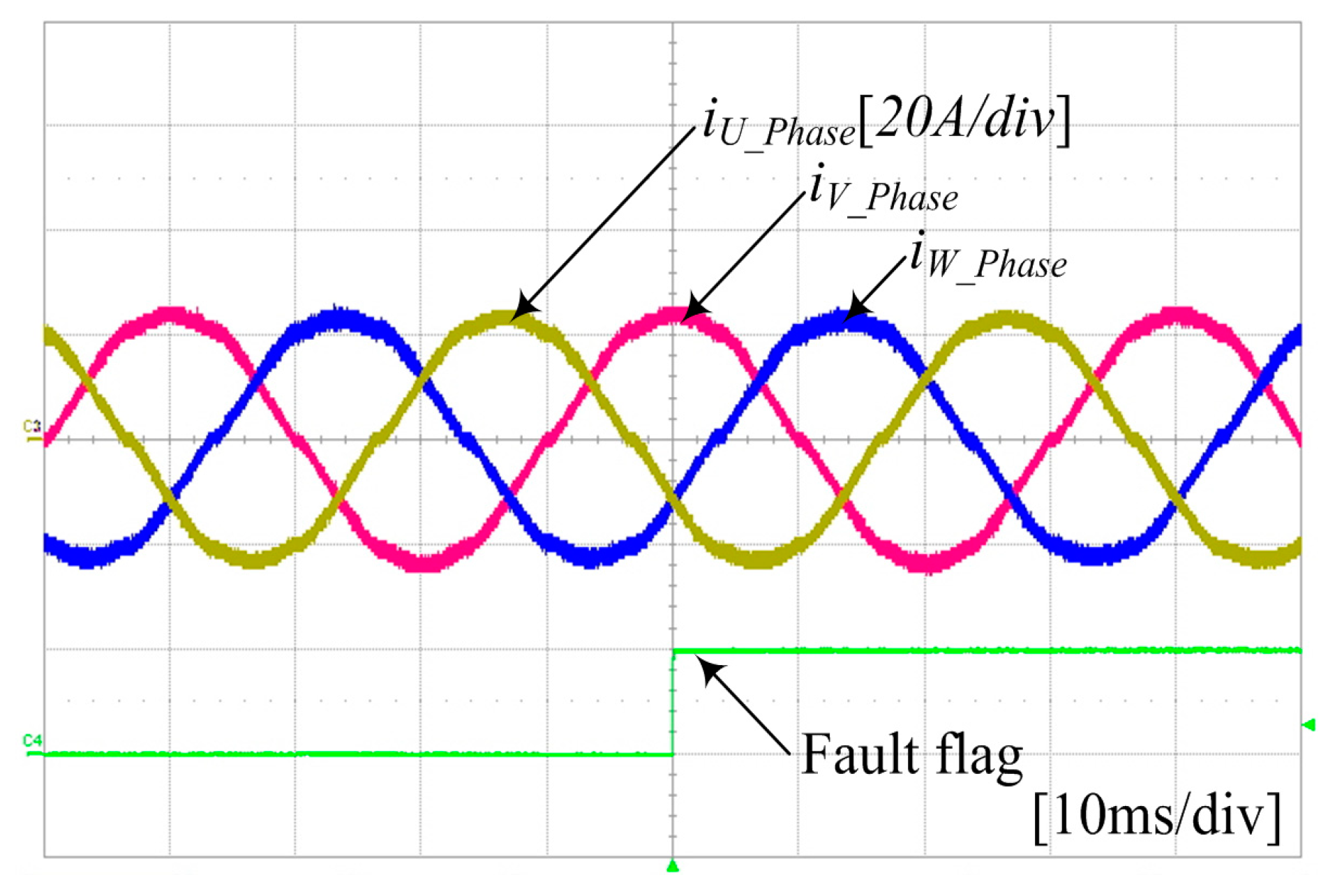
Figure 27 shows the line-to-line voltage and fault flag waveform when using the conventional neutral-point voltage-shifting control. As shown in the figure, the line-to-line voltage waveform shows the characteristics of the three-phase equilibrium even in the fault situation. The phase current on the load side is shown in
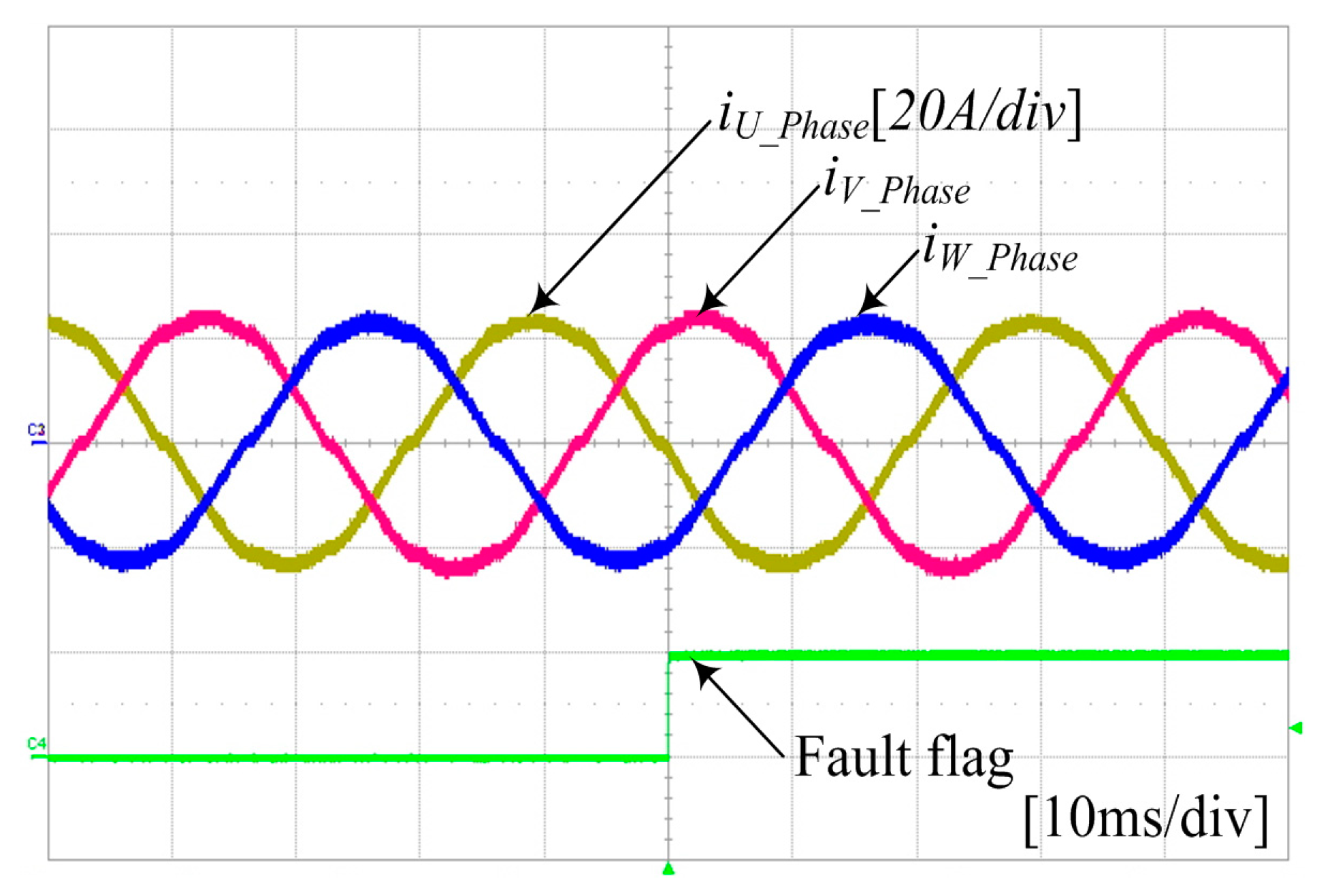
Figure 28.
Even if one stack fails, as shown in
Figure 28, the waveform of the phase current also appears as a three-phase equilibrium when three-phase equilibrium of the line-to-line voltage is obtained through the use of the neutral-point voltage-shifting control.
Figure 29 shows the individual stack output power waveform when applying the conventional neutral-point voltage-shifting control. When the first stack of the U phase fails, as shown in
Figure 29, the output power of the second stack on the U phase and the output power of the fourth stack on the V phase are different from each other.
As a result, the V phase provides 18.2% more output power than the failed stack. This result is similar to the result of the simulation that output 20.4% more power.
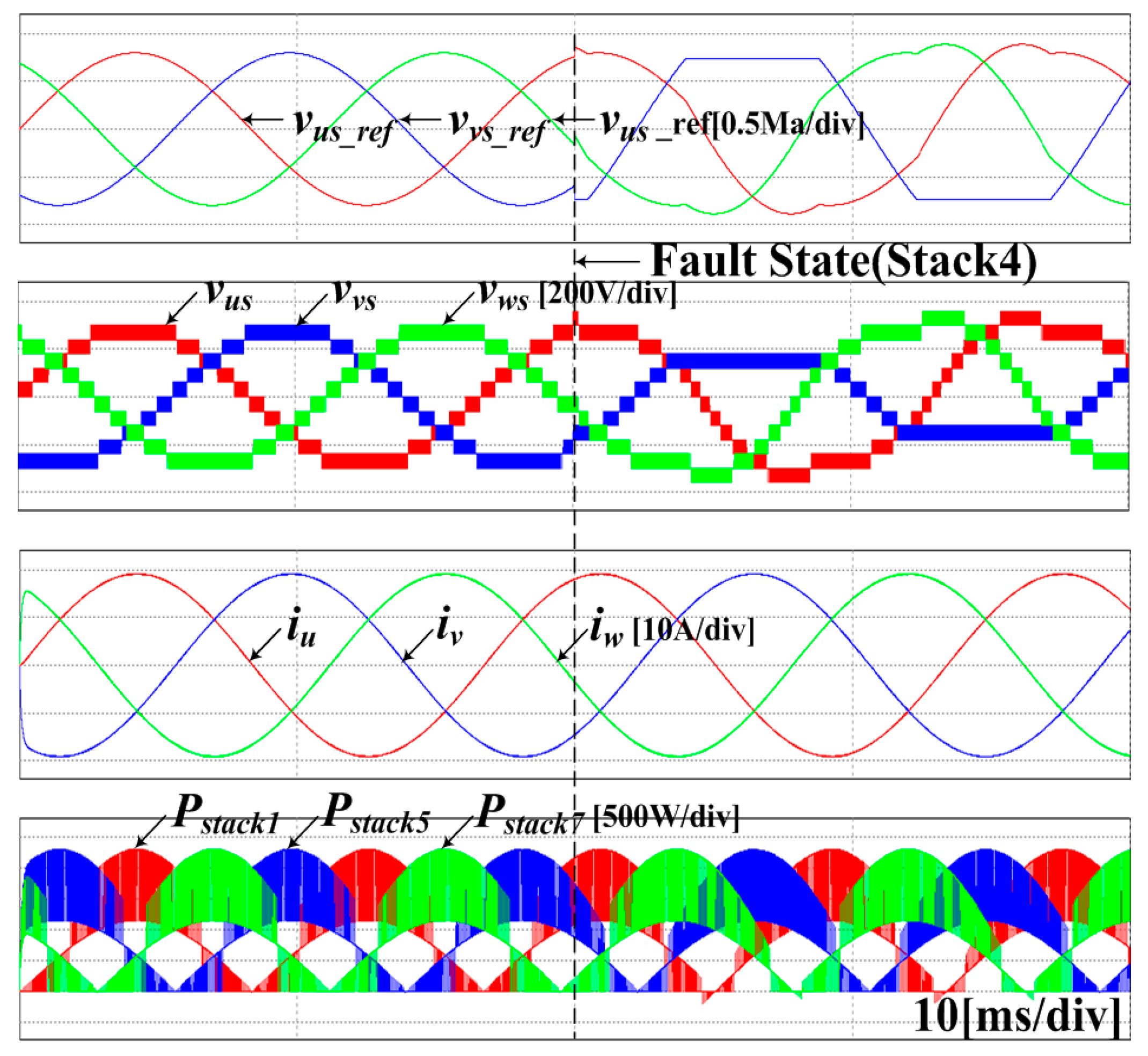
Figure 30 shows the phase voltage and the fault flag waveform when the proposed neutral-point voltage-shifting control is applied. In the case of a fault situation, the proposed control is also applied so as to instantly convert the phase voltage modulation, and thus the neutral-point voltage-shifting control can be seen.
Figure 31 shows the line voltage waveform when using the proposed neutral-point voltage-shifting control. Similar to the conventional neutral-point voltage-shifting control, three-phase equilibrium is established for the line-to-line voltage even in the fault situation. In addition, the line-to-line voltage waveform is similar to the simulation.
Figure 32 shows the phase current waveform applying the proposed neutral-point voltage-shifting control. In the case of applying the conventional neutral-point voltage-shifting control, the phase current maintains three-phase equilibrium in the same way as shown in
Figure 28.
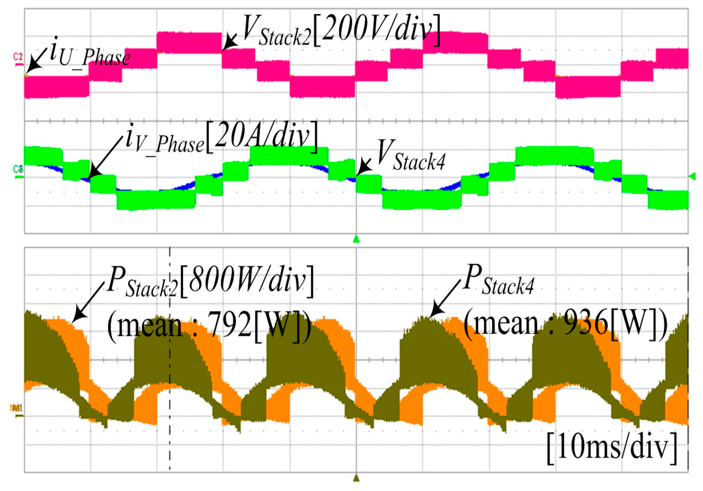
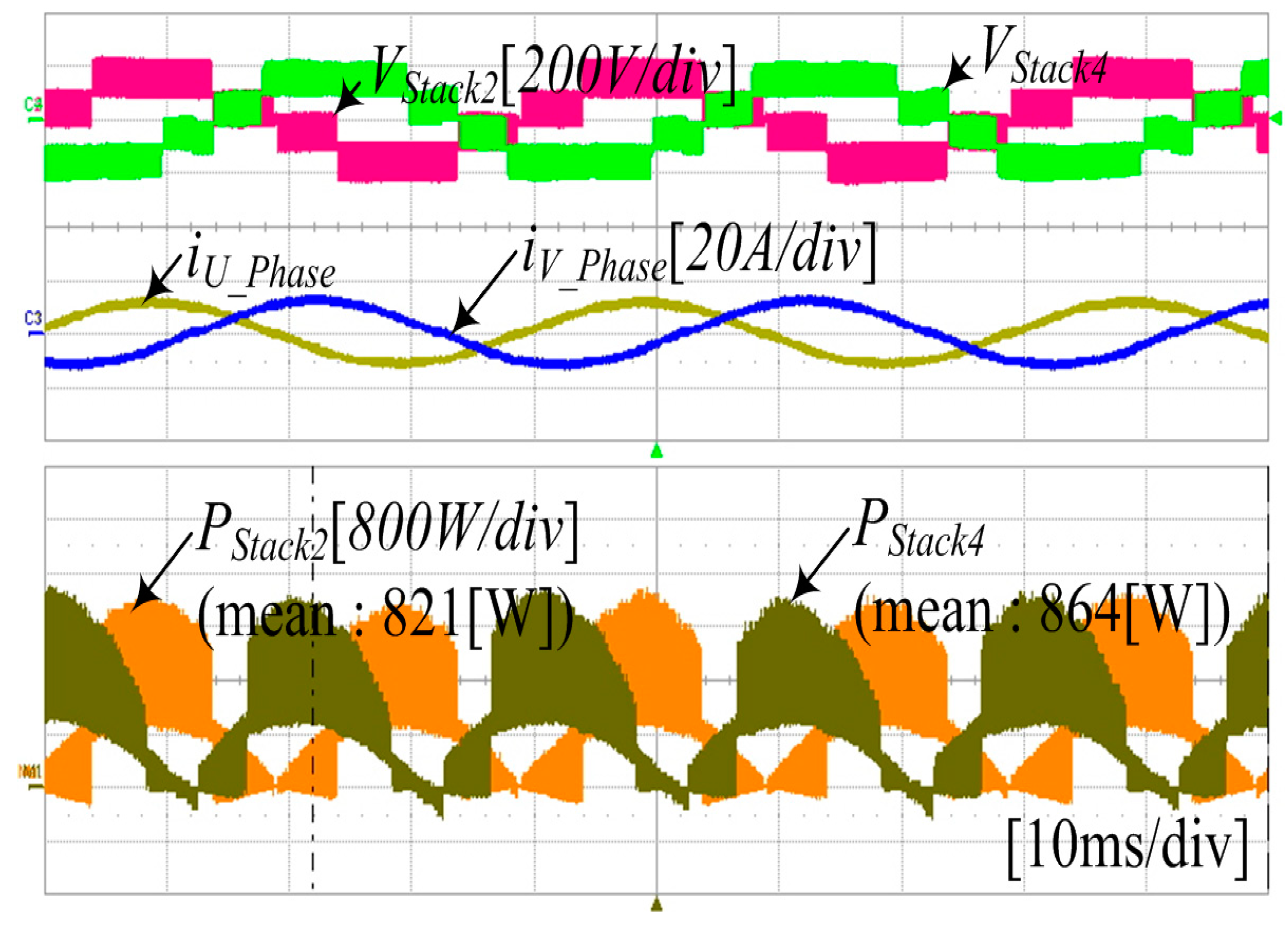
Figure 33 shows the experimental waveforms of the output voltages, phase currents, and output powers of the second and fourth stacks applying the proposed neutral-point voltage-shifting control. When the proposed control is applied, the experimental results show that the output power is only about 5% different from the conventional neutral-point voltage-shifting control. In that way, it is confirmed that the power difference of about 18.7% is reduced to about 7.4% through the simulation, and the power difference of about 16.6% is reduced to about 5.1% by the experiment. Therefore, the effectiveness and feasibility of the proposed neutral-point voltage-shifting control can be verified.


