1. Introduction
Modern CMOS technology scaling is no longer just a matter of shrinking physical dimensions. A key to down scale the equivalent oxide thickness (EOT) in recent technologies is the replacement of classic poly-Si gate/SiO gate stack with a high-k dielectric/metal gate stack. Given the tremendous interest in scaled RF CMOS and RF system-on-chip that integrates digital and RF functions, it is necessary to examine the RF performance of the core transistors in these scaled technologies.
In this work, we investigate two-tone intermodulation linearity in a 28 nm high-k/metal gate RF CMOS technology [
1], characterized by the intermodulation intercept. Both second and third order intermodulation intercept
and
are measured. We focus on
as it is more relevant. Third order intermodulation products are close to the fundamental frequencies of interest and cannot be filtered out [
2]. Mixing of adjacent channel interferers produces undesired output in the frequency band of interest. Third order nonlinearities are also responsible for desensitization and cross-modulation.
From a gate capacitance perspective, poly depletion effect is no longer present with the use of metal gate, the change of gate-to-source capacitance
with gate voltage is less in strong inversion, and linearity should improve compared to poly-gate transistors according to [
3]. That analysis, however, assumed velocity saturation at the source, which is not the case in today’s advanced CMOS. Scaling, and the associated changes in doping, effective oxide thickness, strain are all expected to change device
characteristics as well as the various transconductance nonlinearities, output conductance nonlinearities, and cross nonlinearities.
Harmonic gate voltage
of 28 nm RF CMOS devices has been recently examined using third-order derivative of
data [
4]. However, no experimental RF measurement of
has been reported. Previous investigations using Volterra series analysis [
5] showed that such estimation using third-order transconductance nonlinearity alone is not sufficient in characterizing transistor
. Drain conductance nonlinearity as well as cross terms involving partial derivatives of
with respect to both
and
are also important [
6]. Typical compact model parameters are extracted by fitting DC
I-
V curves and sometimes first order derivatives. A good fitting does not necessarily guarantee good accuracy of higher order derivatives, which are difficult to evaluate experimentally due to the increase of numerical and experimental error in differentiation. Direct RF intermodulation measurements are therefore necessary, which we present below, together with simulations using a compact model with DC
I-
V and Y-parameter calibration. As
in RF measurements is determined using RF power of the source voltage, the result in general depends on frequency, and cannot be directly compared with traditional gate voltage
that is defined using the gate voltage.
We propose below a new figure-of-merit that can be extracted from RF measurements so that meaningful comparison with traditional intermodulation gate voltage can be made with ease. The new figure-of-merit accounts for both and related nonlinearities, and reduces to traditional intermodulation gate voltage when all of the related intermodulation products are neglected.
2. Tested Technology and Measurement System
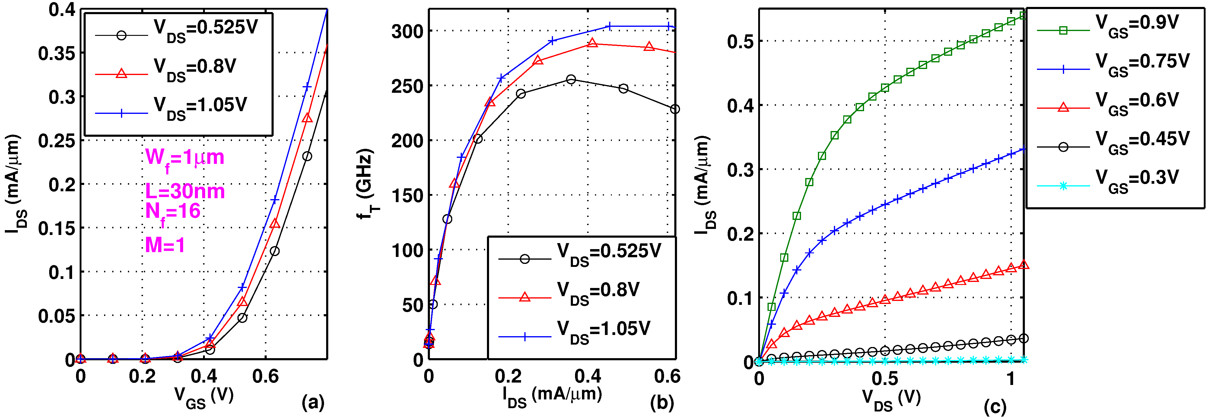
Figure 1a shows typical
characteristics of a 30 nm device from the examined 28 nm technology.
Figure 1b shows measured cut-off frequency
as a function of
. A 304 GHz peak
is reached at 0.45 mA/ μm at
1.05 V.
Figure 1c shows typical
characteristics.
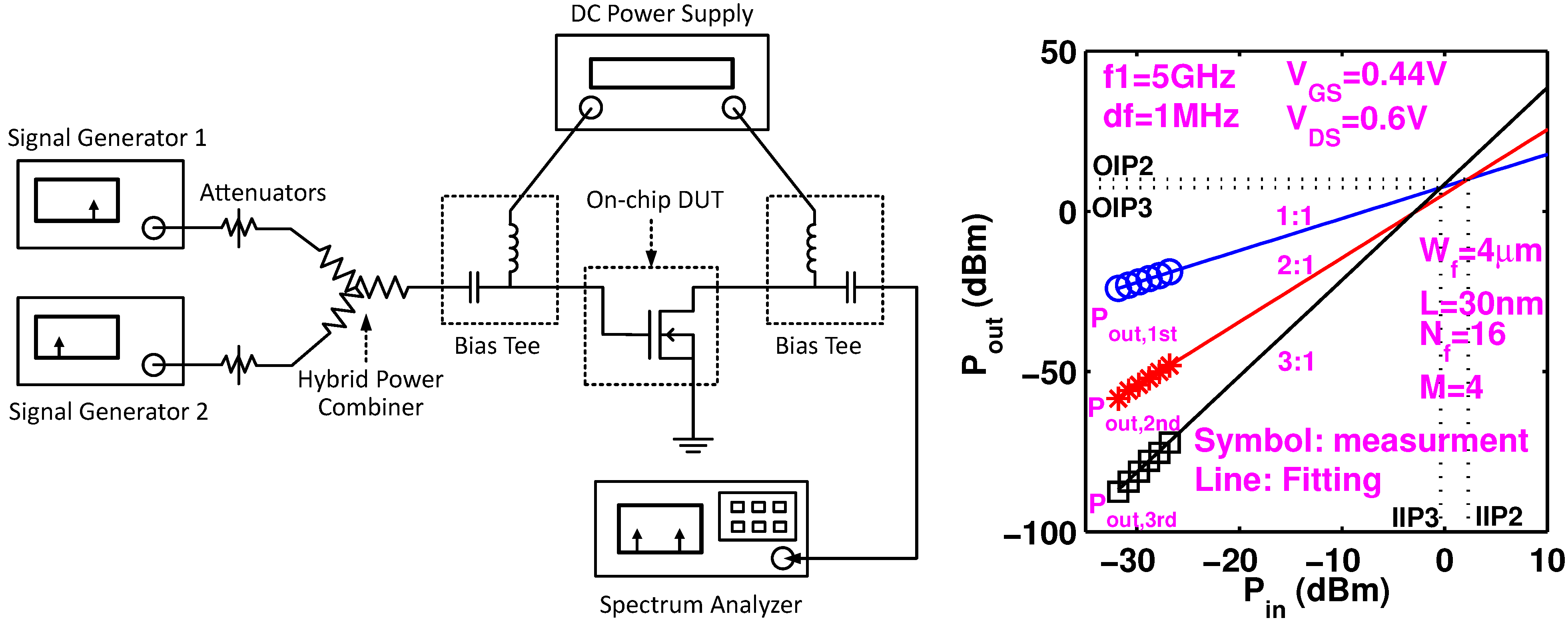
Figure 2a shows the experimental setup used, which is similar to the setup in [
7]. Broadband 50 Ω terminations are used so that they do not filter out the second order harmonics which may remix with the fundamental output to produce third order intermodulation (
). Devices are probed on-wafer using Cascade Infinity GSG probes. Two Agilent signal sources are synchronized and combined using a power combiner to produce a two tone input. Attenuators are used to reduce the intermodulation within the sources. Automatic level control in the sources is turned off to minimize intermodulation generated by the sources. An HP-6625 power supply is used to provide precision DC biases. A spectrum analyzer is used to measure the output spectrum. Power meters are used for calibration of power loss on cables and probes. Analyzer setting is optimized for each measurement to minimize analyzer
and maximize signal to noise ratio. For each bias point and frequency, the input power is swept and the third order intercept is obtained by extrapolation. The analyzer setting is optimized dynamically for each input power level. The measurement system intermodulation is verified to be well below the intermodulation from the device under test. The upper and lower
are the same in our measurements.
Figure 1.
Measured (a) versus ; (b) versus and (c) versus .
Figure 1.
Measured (a) versus ; (b) versus and (c) versus .
Figure 2.
(a) Measurement setup and (b) extrapolation illustration for and .
Figure 2.
(a) Measurement setup and (b) extrapolation illustration for and .
Figure 2b illustrates how
and
are determined for a 30 nm device biased at
0.44 V,
0.6 V. Device total width is 256 μm. Gate finger width
is 1 μm, number of finger
is 16, and multiplicity
16. At low
, first order output
increases linearly with
at a slope of 1:1, while the third and the second order intermodulation output (
and
) increase at slopes of 3:1 and 2:1, respectively.
is obtained as the extrapolated intercept of
and
in a region of
where the ideal slopes are observed. The input and output powers at
are denoted as
and
. Their difference is gain. Similarly, we can obtain
and
from the extrapolation intercept of
and
.
3. Results and Analysis
As mentioned earlier, in RF measurement, the intercept point is defined using RF input power. The input third order intermodulation intercept point, , is thus dependent on frequency, because of finite source impedance, which for our case, is a 50 Ω resistance. For a given RF input power, the RF gate voltage varies with frequency, as transistor input impedance varies with frequency. For analysis as well as estimation of at another design frequency from measurement at one frequency, it is desirable to find a figure-of-merit that does not depend on frequency. Such figure-of-merit is more useful if it can relate to the traditional figure-of-merit, gate voltage , but also include effects of drain voltage related nonlinearities. We derive such a figure-of-merit below using Volterra series analysis.
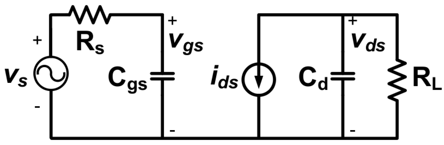
A simplified equivalent circuit as shown in
Figure 3 is used. Gate-drain capacitance (
) is omitted, as the result is much simpler and sufficient for most purposes [
5].
50 Ω.
is gate-to-source capacitance.
is drain capacitance.
50 Ω is load resistance.
Figure 3.
Simplified equivalent circuit used for derivation using Volterra series.
Figure 3.
Simplified equivalent circuit used for derivation using Volterra series.
is nonlinear drain current:
and
are transconductance and output conductance.
,
,
,
and
are nonlinearity coefficients that relate to higher order partial derivatives as defined in [
8] using Taylor expansion. For instance,
Using the nonlinear current source method,
can be derived [
5]:
where
.
through
are functions of nonlinear output conductance, its high order terms and cross terms with transconductance nonlinearity as follows:
through
are given by:
with
and
.
A close inspection of the Volterra series based derivation details shows that at the intermodulation
point, the first order
has an amplitude of:
For typical transistor sizes of interest, the Δ term is found to have a negligibly weak frequency dependence, making nearly frequency independent in practice. We thus propose to use as a figure-of-merit as it includes output conductance effect, and is more general than the traditional defined solely using and . The designation in the subscript refers to the fact that this is the amplitude at the intercept. The value of , however, is clearly a function of the dependence of , through the Δ term.
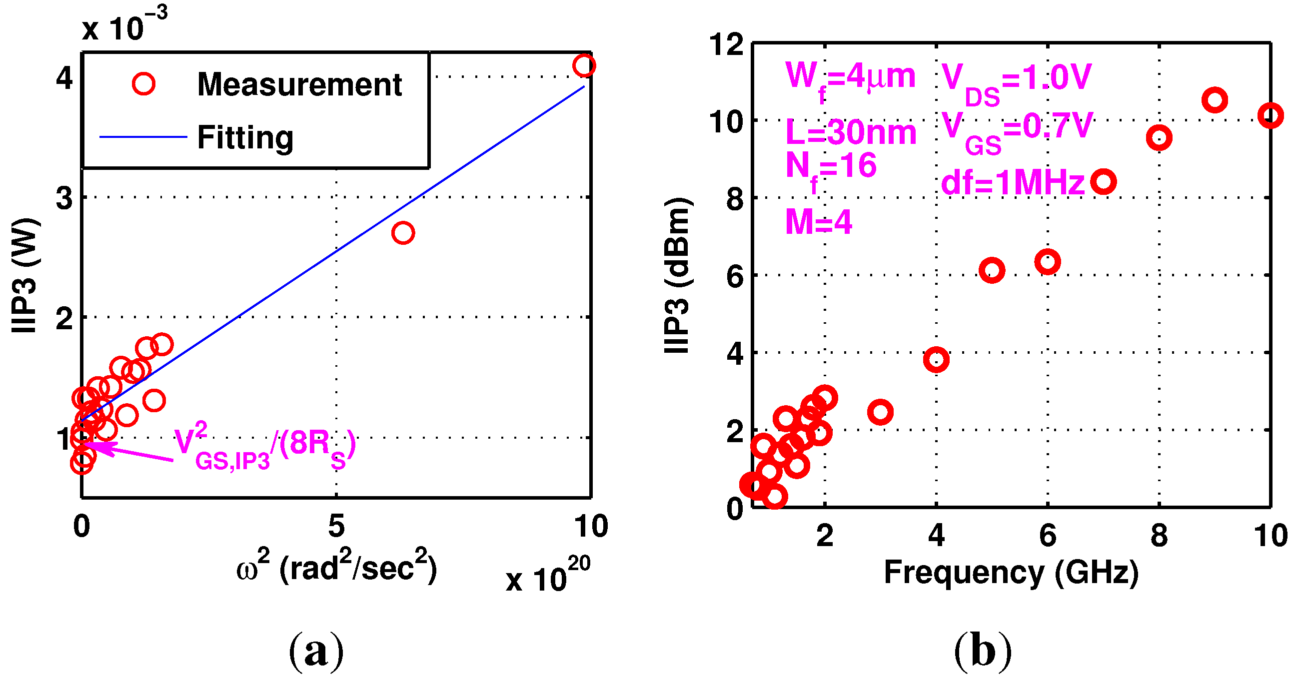
Using
, Equation (
4) can then be rewritten as
Equation (
18) indicates that
increases linearly with
and
can be obtained experimentally by plotting measured
as a function of
, as shown in
Figure 4a. A linear fitting is made. The intercept with the
axis gives
. Note that the unit used for
is watt instead of dBm. As measured
in dBm is shown in
Figure 4b. The device has a drawn gate length of 30 nm.
4 μm.
16. Multiplicity
4. The total width
256 μm.
0.7 V and
1.0 V. Measurement frequency ranges from 100 MHz to 10 GHz. Within measurement uncertainty, the data shows an expected linear dependence on the square of fundamental angular frequency. This linear dependence of
on
is found to be valid for other bias points as well. The slope is given by
from which
can be extracted. The
calculated is fairly close to that extracted from S-parameter measurements, thus supporting the validity of the proposed technique.
If we ignore the Δ term that originates from the
dependence of
,
reduces to
Figure 4.
Frequency dependence of at 0.7 V and 1.0 V. (a) Measured in watt versus ; (b) Measured in dBm versus frequency.
Figure 4.
Frequency dependence of at 0.7 V and 1.0 V. (a) Measured in watt versus ; (b) Measured in dBm versus frequency.
This is essentially the
one would get if transistor drain current depends on
only. This
for intermodulation distortion differs from the third order harmonic distortion
in [
4,
9] by a constant.
The transistor model used to evaluate the derivatives needed in Equation (
4) is a
PSP model, with initial parameter values for base line digital CMOS transistors of the same technology. In this work, device model parameters are tuned to better fit the
I-
V characteristics and S-parameters.
Figure 5a,b compare simulated
versus with measurement using linear and log
scales, respectively. Good agreement is achieved. To simulate
, quasi periodic steady state (QPSS) analysis is used in
Cadence SpectreRF to calculate two-tone large signal behavior [
10]. For each bias point, a series of input power level is swept. The output is plotted using ipnVRI function to ensure the extrapolation point for
is within the linear range, in the same manner
is determined in measurement illustrated earlier in
Figure 2b.
Figure 6a shows both measured and simulated
at 5 GHz as a function of
at
0.6 V for the same device in
Figure 5. Measurements and simulations are also made at 2 and 10 GHz. At each
, from frequency dependence of
, a
is extracted. From 0.5 to 0.7 V, simulated
is higher than measured
by as much as 3.8 dB. This indicates that simulated
for such technologies may be optimistic. In future work, model parameters can be further optimized to see if
can be better fitted. To our knowledge, there are no direct knobs to turn to tune higher order derivatives in compact models. Improvement of
simulation may require new improvements of the model formulation itself in addition to better parameter extraction and optimization.
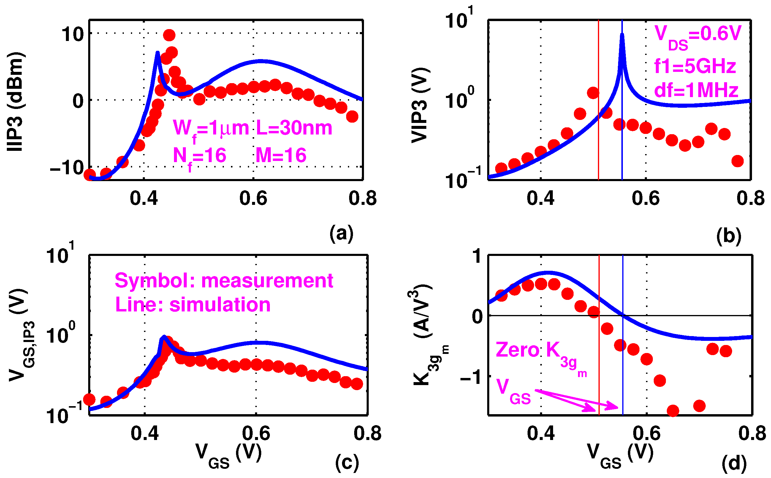
Figure 6b shows the
calculated from
and
using Equation (
19). Fitting of
, which is determined by the first and third order derivatives of
-
, is clearly worse than the fitting of
-
itself shown earlier in
Figure 5.
Figure 6c,d show
and
as a function of
. The
0 point is clearly different from the measured
and
peak positions. The peak
is 55 mV lower than the peak
. As was observed in 90 nm technology [
5],
does not correctly predict the linearity sweet spot, due to omission of the Δ term. Around
0.6 V,
and the traditional
are close to each other, as the Δ term is small. Beyond its peak,
drops to a valley and starts rising slowly. However, when
0.65 V, as the device gets closer to linear operation region,
shows a slight decrease.
Figure 5.
Comparison of simulated versus with measurement on (a) linear and (b) log scales at 0.6 and 1.0 V.
Figure 5.
Comparison of simulated versus with measurement on (a) linear and (b) log scales at 0.6 and 1.0 V.
Figure 6.
(a) (b) (c) and (d) as a function of at 0.6 V.
Figure 6.
(a) (b) (c) and (d) as a function of at 0.6 V.
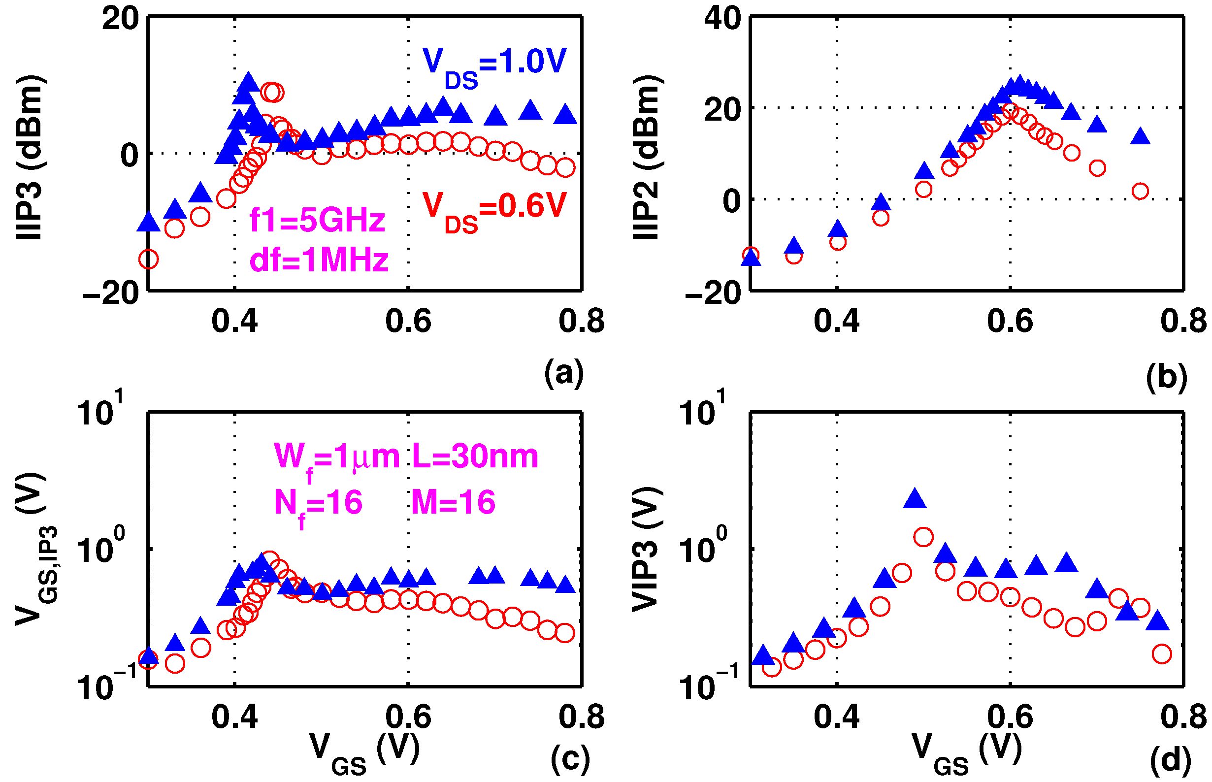
Figure 7a–d show measured
,
,
, and
as a function of
at
0.6 and 1.0 V. The same device as in
Figure 6 is used. As can be seen from
Figure 7a,
curves at high
are shifted towards low
direction due to decreased threshold voltage, a consequence of drain induced barrier lowering. In strong inversion region, at the same
, a higher
results in a higher
. For instance, at
0.8 V,
increases by 7.7 dB when
increases from 0.6 to 1.0 V. As shown in
Figure 7b,
has a clear peak, though not as sharp as
, around
0.6 V, in strong inversion. If both high
and high
are desired, the transistor should be biased around
0.6 V, which is approximately 200 mV above threshold voltage. A comparison of
Figure 7c,d shows that the
dependence of
and hence
is insufficiently captured by
, due to lack of
related terms, as expected.
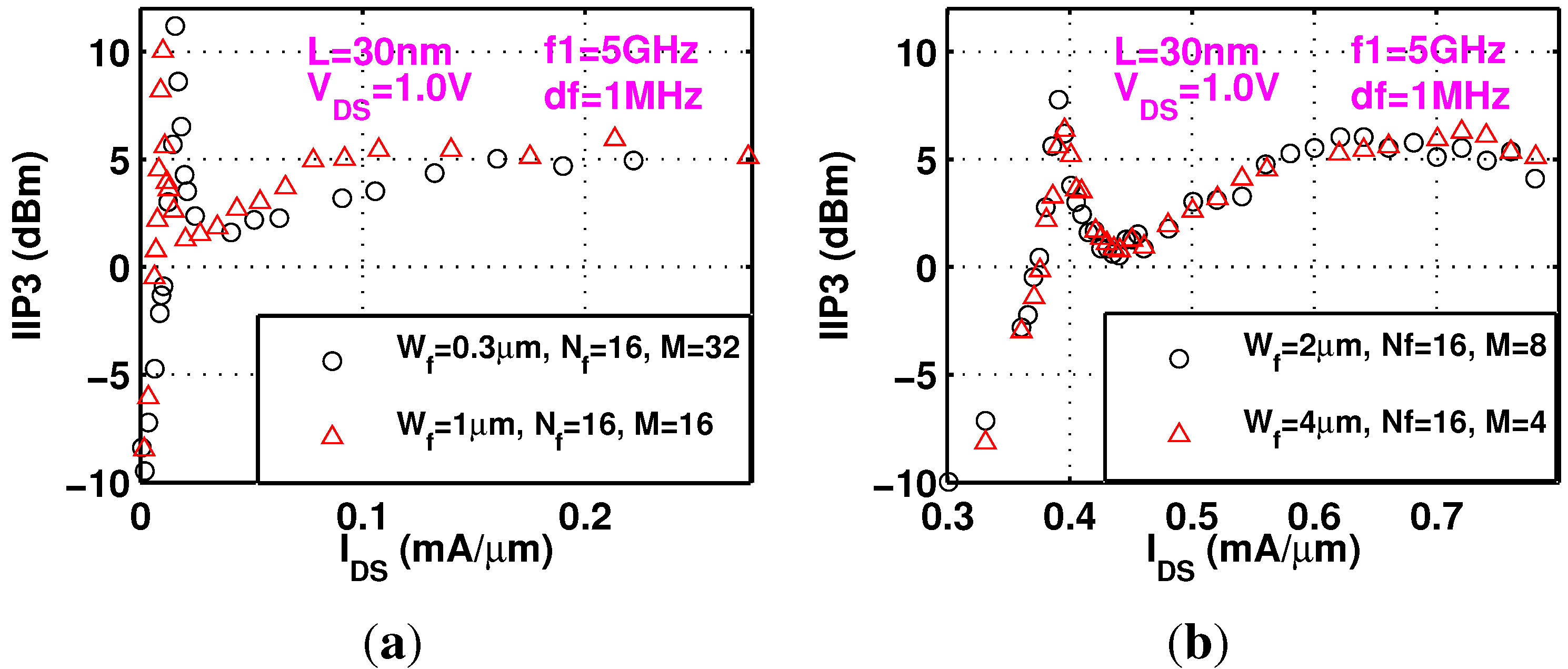
Figure 8a shows measured
at 5 GHz for devices with
153.6 and 256 μm. Note that the device finger widths are 0.3 and 1 μm respectively. At both very low and high
, a large device gives a large
. Both peak
value and peak
decrease with device width. Narrow width effect clearly plays a role in affecting the position of the linearity peak.
Figure 8b shows measured
as a function of
for two 30 nm MOSFETs with the same total width of 256 μm. As the device finger widths are both large, 2 and 4 μm respectively, no narrow width effect is observed, and
is largely the same for the two devices as expected.
Figure 7.
Measured (a) ; (b) and (c) and (d) as a function of for different .
Figure 7.
Measured (a) ; (b) and (c) and (d) as a function of for different .
Figure 8.
Measured width impact on . (a) Measured at 5 GHz for two 30 nm devices with different total width; (b) Measured as a function of for two 30 nm devices with same total width.
Figure 8.
Measured width impact on . (a) Measured at 5 GHz for two 30 nm devices with different total width; (b) Measured as a function of for two 30 nm devices with same total width.

