

Article

Light-Load Efficiency-Optimized Variable Duty Cycle Control Strategy for SP-Compensated Wireless Power Transfer Systems

Department of Electrical Engineering, National United University, Miaoli 36003, Taiwan
*
Author to whom correspondence should be addressed.
Electronics 2026, 15(9), 1908; https://doi.org/10.3390/electronics15091908
Submission received: 12 April 2026 / Revised: 26 April 2026 / Accepted: 29 April 2026 / Published: 1 May 2026

Abstract

This paper presents an efficient control strategy for a wireless power transfer (WPT) system based on a series–parallel (SP) compensation topology, specifically optimized to enhance efficiency under a wide load range, including light-load conditions. The system employs a half-bridge inverter on the transmitter side and a semi-active rectifier (SAR) on the receiver side to achieve zero phase angle (ZPA) operation. Zero voltage switching (ZVS) is achieved by synchronizing and phase-adjusting the SAR switching signals with the rectified input voltage, thereby effectively reducing switching losses. Furthermore, a perturbation and observation (P&O)-based variable duty cycle (VDC) control is applied to the half-bridge inverter to dynamically optimize the light-load efficiency, thereby enhancing efficiency when conventional fixed duty methods underperform. The proposed control strategy is implemented using a TI TMS320F28335 digital signal processor. Experimental results demonstrate that the method significantly improves system efficiency at light loads while maintaining high performance at heavy loads, verifying its practical feasibility for diverse WPT applications.

1. Introduction

In contrast to conventional wired transmission systems, wireless power transfer (WPT) technology enables the transmission of energy from the source to the sink without the need for physical conductors or galvanic contact. Leveraging its intrinsic advantages of convenience and non-contact operation, WPT technology has achieved widespread deployment in various daily applications. The scope of WPT applications continues to expand, encompassing examples ranging from low-power mobile charging devices to high-power electric vehicle charging systems, as extensively documented in ref. [1]. However, existing WPT systems still face numerous technical constraints. A primary bottleneck is the low output power and transmission efficiency [2,3], an issue that is particularly pronounced in low-power charging applications such as smartphones, tablets, and E-bikes. In response to these drawbacks, this paper proposes an approach to increase the efficiency of low-power wireless charging systems based on relevant literature.
To address the issue of increasing the output power and efficiency of WPT systems, a solution involving an external boost–buck converter is presented in refs. [4,5]. By incorporating the perturb and observe (P&O) method into the boost–buck converter, maximum power point tracking and load matching are achieved, thereby enabling the system to maintain maximum power transfer. However, this circuit topology necessitates the addition of a DC-DC converter to the original WPT architecture. This results in an increased circuit volume, higher component count, higher cost, and increased complexity of system control.
The method of using variable capacitors or variable inductors in the resonant circuit is proposed [6,7,8,9]. This design enables the system to instantly adjust its resonant frequency in response to variations in the input power source or load, allowing the output to operate in constant current (CC) mode. Consequently, the system operates at the resonant frequency, thereby realizing optimal output power and system efficiency. However, the addition of variable capacitors or variable inductors requires extra circuit control, which increases the number of components used and raises the overall system complexity.
A full-bridge inverter control method is presented in ref. [10], featuring switching capabilities between full-bridge, phase-shift, and half-bridge modes. This strategy introduces a half-bridge mode for light-load operation, complementing the basic full-bridge and phase-shift control modes, thereby enhancing the circuit’s efficiency at light loads. Another approach involves dynamically switching the full-bridge inverter and the synchronous rectifier among full-bridge, hybrid-bridge, and half-bridge modes [11]. This strategy aims to achieve zero voltage switching (ZVS) and minimize the circulating current induced by reactive power, thereby enhancing overall system efficiency. For power levels under 1 kW, the system is configured to run exclusively in the half-bridge mode for both stages. Ref. [12] utilizes the perturbation and observation (P&O) algorithm to adjust the phase shift of the half-bridge inverter’s control signals. This approach reduces the input power, thereby enhancing the system efficiency.
To minimize conduction losses in power switching elements, various control strategies have been proposed in academia. Refs. [8,11,13] propose a method to conduct both lower-arm switches of the semi-active bridge rectifier (SABR) simultaneously when the resonant circuit’s output voltage is zero. This operation initiates a short-circuit mode to eliminate the conduction losses caused by the MOSFET body diodes. Furthermore, refs. [5,9,14,15] employ a strategy where the lower-arm switch of the semi-active bridge rectifier is activated after a specific phase delay. This ensures that the power switching elements achieve ZVS characteristics, reducing the conduction losses of both the switches and diodes, and thus achieving the goal of increasing output power and efficiency.
The main contributions of this paper are as follows. This paper proposes a control strategy for SP-compensated wireless power transfer (WPT) systems. The goal is to improve efficiency across a wide load range, especially under light-load conditions, without adding power-conversion stages or tunable reactive components. A perturbation and observation (P&O)-based variable duty cycle method is developed for the half-bridge inverter. This method dynamically regulates inverter operation and optimizes efficiency under varying load conditions. In addition, a coordinated control scheme between the transmitter-side inverter and the receiver-side semi-active rectifier (SAR) is implemented. This coordination achieves zero voltage switching (ZVS) and zero phase angle (ZPA) operation, reducing switching and conduction losses. Finally, a hardware prototype is constructed to experimentally validate the proposed control strategy. The results show improved efficiency at light loads and stable performance over a wide load range.
Table 1 summarizes the comparison of reported WPT control strategies. As illustrated in Table 1, the proposed control strategy stands out as a simplified hardware solution with streamlined control logic. By optimizing the design trade-off between primary side gain and switching dissipation, the system minimizes costs while attaining a higher efficiency-to-complexity ratio than conventional MPC-based or multiswitch high-power systems. This makes the proposed method highly viable for real-world implementation.

2. Analysis and Design of Proposed SP-Compensated Power Transfer System

2.1. Circuit Analysis

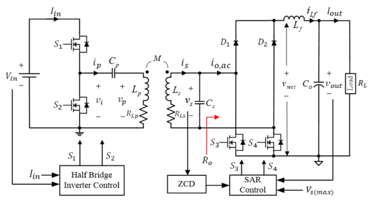
Figure 1 illustrates the architecture of the proposed WPT system. Electrical energy is transferred to the SP-compensated resonant circuit via a high-frequency square wave generated by a half-bridge inverter. This process induces electromagnetic induction in the coupled coils, transmitting power via the magnetic field to the receiving side. Subsequently, the AC voltage is converted into a DC output voltage by passing through a semi-active bridge rectifier and an LC filter.
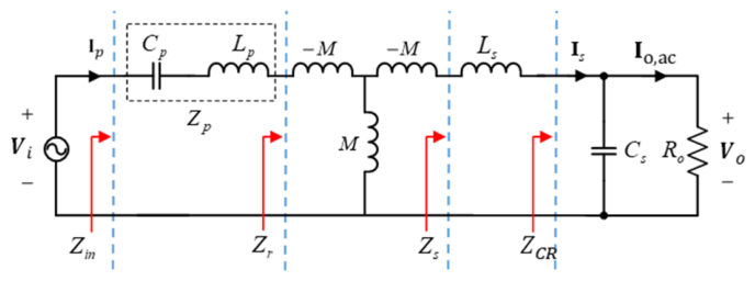
The load is modeled as a simple resistive load to facilitate the creation of the equivalent circuit, which is depicted in Figure 2. The necessary conversion of the input DC voltage and the load resistance into their corresponding AC representations is given by the equations that follow:
V i n = 2 V d c π 0 °
R o = π 2 8 R L
To minimize the apparent power demand on the input source and eliminate reactive power for maximum power transfer capability, the impedance of the resonant circuit must exhibit zero phase impedance [16,17]. In circuit analysis, after converting all DC components into AC components, the coupled inductor in Figure 1 is replaced with a T-equivalent circuit. Assuming the coils are ideal, which means there is no internal coil resistance, the equivalent circuit can be simplified to the circuit shown in Figure 2. In this equivalent circuit, the relationship between the impedances is as follows:
Z C R = R o 1 + j ω C s R o         Z s = j ω L s + Z C R           Z r = ω 2 M 2 Z s                   Z p = j ω L p + 1 j ω C p       Z i n = Z p + Z r              
At the resonant frequency, the impedance of the resonant circuit must achieve ZPA to eliminate the reactive power at the system output and maximize power transfer capability. Therefore, compensation capacitors need to be designed to cancel out the inductive component of the coils within the resonant circuit. To ensure the secondary side load appears resistive, the inductance and capacitance values in the compensation circuit must mutually cancel each other [16]. The equations for L s ,   C s and ω o have been found.
j ω o L s = j ω o C s ω = 1 L s C s = ω o = 2 π f o
Rearranging (3), Z i n can be obtained:
Z i n = j ω L p + 1 j ω C p + ω 2 M 2 ( 1 + j ω C s R o ) j ω L s ω 2 L s C s R o + R o
Substituting (4) into (5) and simplifying yields
Z i n = j ω L p + 1 j ω C p + M 2 R o L s 2 j ω M 2 L s
To eliminate the system’s reactive power, the ZPA condition must also be met. Therefore, the imaginary part of Z i n must be zero. Utilizing the aforementioned conditions, the relationship between C p and other system parameters can be derived:
C p = L s ω o 2 L p L s M 2 = L s 2 C s L p L s M 2
The calculation formulas are provided in ref. [18] for the phase θ p relationship between I p and V i and the phase θ s relationship between I s and.   V i . These two phase angles are related to the system parameters as follows:
θ p = tan 1 R L 2 + ω L s 1 ω C s 2 ω L p 1 ω C p ω 2 M 2 ω L s 1 ω C s R L 2 + ω L s 1 ω C s 2 R p + ω 2 M 2 R L
θ s = tan 1 ω 2 M 2 + R p R L ω L p 1 ω C p ω L s 1 ω C s ω L s 1 ω C s R p + ω L p 1 ω C p R L
Substituting (4) into (8) and (9) yields θ p and θ s at the resonant frequency.
θ p = tan 1 R L ω L p 1 ω C p R L R p + ω 2 M 2
θ s = tan 1 ω 2 M 2 + R p R L ω L p 1 ω C p R L
From (10) and (11), it can be seen that θ p + θ s = 90 ° . Due to the circuit design requirement for a zero phase angle, where θ p = 0 ° , it consequently follows that θ s = 90 ° . The coupling capacitor in the series–parallel compensation circuit is used to compensate for θ s , as described in (4). Consequently, the net compensated phase difference becomes zero, allowing the resonant circuit to achieve the condition of a ZPA for the overall circuit impedance.
Applying Kirchhoff’s voltage law (KVL) to the circuit analysis of Figure 2, the relationship between the voltages and currents in the circuit can be derived:
V i = Z p I p j ω M I s
Z s I s j ω M I p = 0
I o = I s × 1 1 + j ω C s R o
After simplifying (12)–(14), the relationship between the input voltage V i , the output voltage V o , and the secondary side AC current I s is obtained:
V i = I s Z p Z s j ω M j ω M
V o = I s R o 1 + j ω C s R o
Dividing (15) by (16), the system voltage gain G v is obtained as:
G v = V o V i = j ω M R o ( 1 + j ω C s R o ) ( Z p Z s + ω 2 M 2 ) = j ω M Z C R Z i n Z s
Substituting (4) into (17), the voltage gain can be simplified to
G v j ω o = V o j ω o V i j ω o = j ω M × Z C R j ω o Z i n j ω o × Z s j ω o = j ω o M R o L s 2 j ω o L s R o M 2 = L s M
From (18), it can be observed that, under the resonant frequency condition, the voltage gain ( G v ) is dependent on the system parameters L s and M. As the resonant circuit employed in this paper does not account for misalignment or displacement issues, the self-inductance and mutual inductance parameters of the coils are assumed to be fixed. Consequently, the SP-compensated topology exhibits the characteristic of providing a constant output voltage.

2.2. Parameter Design

The resonant frequency is set to 100 kHz. Since hardware dimensions constrain the coupled coils, the coil winding is performed first, and the coil impedance is measured. Subsequently, the estimated parameters are substituted into (4) and (7) to obtain the corresponding compensation capacitor parameters. The designed system parameters are then recorded in Table 2.
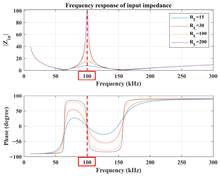
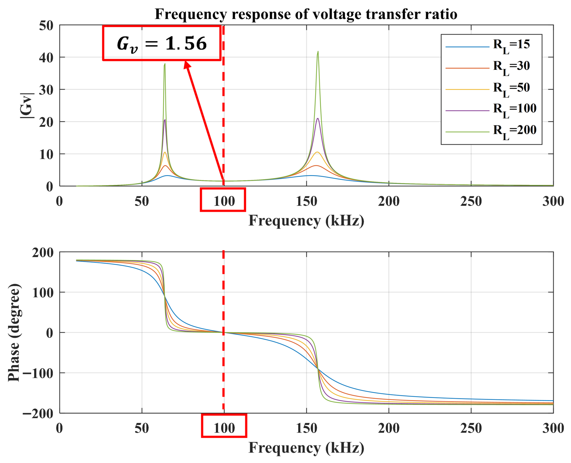
Substituting the parameters from Table 2 into (6) and (18), and then calculating the frequency response, yields Figure 3 and Figure 4. From the input impedance frequency response waveform shown in Figure 3, it can be seen that the input impedance consistently maintains a ZPA at the switching frequency of 100 kHz, regardless of changes in the load resistance magnitude. Observing the voltage gain frequency response shown in Figure 4, it is found that the voltage transfer ratio remains a constant value of 1.56 at the switching frequency and is unaffected by variations in load. This indicates that the parameter design of this system achieves the desired constant voltage output (CVO) characteristic.

2.3. Loss and Efficiency Analysis

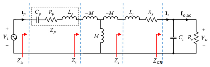
To analyze the system’s efficiency and optimal load resistor, the internal resistances of both the primary and secondary circuits [19] were additionally considered, based on the fundamental circuit shown in Figure 2. The modified equivalent circuit is illustrated in Figure 5. The impedance relationships at this point are as follows:
Z C R = R o 1 + j ω C s R o = R o j ω C s R o 2 1 + ω 2 C s 2 R o 2 = R C R j X C R   Z s = R s + j ω L s + Z C R = R s + R C R + j ω L s X C R Z r = ω 2 M 2 Z s = ω 2 M 2 R s + R C R + j ( ω L s X C R )                   Z p = R p + j ω L p + 1 j ω C p                                             Z i n = Z p + Z r                                                             = R p + j ω L p + 1 j ω C p + ω 2 M 2 R s + R C R + j ( ω L s X C R )
where R C R and X C R are
R C R = R o 1 + ω 2 C s 2 R o 2
X C R = ω C s R o 2 1 + ω 2 C s 2 R o 2
Substituting (19)–(21) into (12)–(16) gives
I p = [ R s + R C R + j ω L s X C R ] V i ( R p + j ω L p + 1 j ω C p ) R s + R C R + j ω L s X C R + ω 2 M 2
I s = j ω M V i R p + j ω L p + 1 j ω C p R s + R C R + j ω L s X C R + ω 2 M 2
I s = V o Z C R V o I s = R o 1 + j ω C s R o
The voltage gain G v can be obtained by dividing (24) by (23).
G v ( j ω ) = V o ( j ω ) V i ( j ω ) = j ω M R o 1 + j ω C s R o { R p + j ω L p + 1 j ω C p R s + Z C R + j ω L s + ω 2 M 2 }
Substituting (4) into (25),
G v j ω o = j ω o M R o 1 + j ω o C s R o { R p R s + Z C R + j ω o L s + ω o 2 M 2 } = j ω o M R o j ω o L s [ M 2 R o + R s L s 2 + R p ]
In practical cases, both R s and R p are much smaller compared to R o and can therefore be neglected. Consequently, (26) can be approximated by retaining only the dominant term associated with R o .
G v j ω o j ω o M R o j ω o L s × M 2 R o L s 2 = L s M
The result indicates that the system retains its voltage-source behavior, with the effect of coil resistance being minimal on its constant voltage output.
The power and efficiency can be determined by the following equations:
P R p = R e I p I p ¯ · R p
P R s = R e { I s I s ¯ · R s }
P o = R e { I s I s ¯ · R C R }
η S P = P o P R p + P R s + P o
Substituting (22) and (23) into (28)–(31) provides the ratios of P R p , P R s , and P o along with the resonant circuit’s efficiency equation.
P R p : P R s : P o = [ ( R s + R C R ) 2 + ( ω L s X C R ) 2 ] R p : ( ω M ) 2 R s : ( ω M ) 2 R C R
η S P = ( ω M ) 2 R C R [ ( R s + R C R ) 2 + ( ω L s X C R ) 2 ] R p + ( ω M ) 2 R s + ( ω M ) 2 R C R
Substituting (4) into (33) gives the resonant circuit efficiency at the resonant frequency:
η S P = ( ω M ) 2 R C R ( R s + R C R ) 2 R p + ( ω M ) 2 R s + ( ω M ) 2 R C R
By taking the derivative of (34) and setting it to zero, the optimal load and its corresponding coefficients are obtained.
η R C R = 0 R C R , o p t = R s 2 + R s ( ω M ) 2 R p
R o , o p t = R C R , o p t 2 + ( ω L s ) 2 R C R , o p t
C s , o p t = L s R C R , o p t 2 + ( ω L s ) 2
Substituting the parameters from Table 2, a value of R C R , o p t = 6   Ω is determined. Subsequent substitution of this value into (2) yields R L , o p t = 15   Ω .
The total system losses must also include the conduction losses of the switching elements and diodes in the half-bridge inverter and the SAR topology, which can be calculated using (38) and (39), respectively
P S i = R d s o n , S i · I S i , r m s 2
P D i = V f , D i · I D i , r m s
The total efficiency of the system is
η t o t a l = P o P R p + P R s + P o + 4 P S i + 2 P D i

3. Control Strategies for Inverters and Rectifiers

3.1. Control Strategy for Half-Bridge Inverters

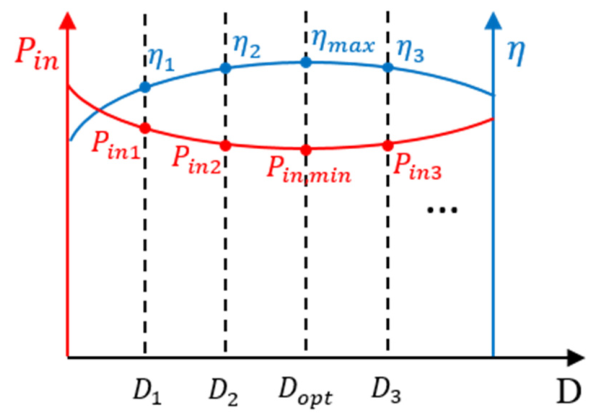
To identify the maximum efficiency point in the WPT system, the control method for the primary side half-bridge inverter in this paper is based on the P&O algorithm [12,20]. Figure 6 illustrates the correlation between input power P i n , system efficiency η , and duty cycle D. By adjusting the conduction period of the inverter switching elements, the objective is to determine the minimum input power P i n , thereby maximizing the system efficiency. The relationship between P i n , the input voltage V i n , and the input current I i n is expressed as follows:
P i n = V i n · I i n
From (41), it can be observed that, when V i n is constant, P i n is directly proportional to I i n . Therefore, by tracking the minimum value of the input current signal I i n , m a x , the minimum input power P i n , m a x can be determined, which subsequently leads to the maximum system efficiency η m a x .
Due to the risk of short-circuiting the primary side circuit if both the upper and lower switches of the half-bridge inverter conduct simultaneously, the maximum duty cycle for both switches is limited to 0.5. Under heavy-load conditions, maximum system efficiency is achieved D = 0.5 . Accordingly, referencing the method in ref. [11], the operating conditions for heavy and light loads are integrated to implement the corresponding mode switching. VDC control is used for light loads. In contrast, fixed duty cycle (FDC) control is employed for heavy loads.
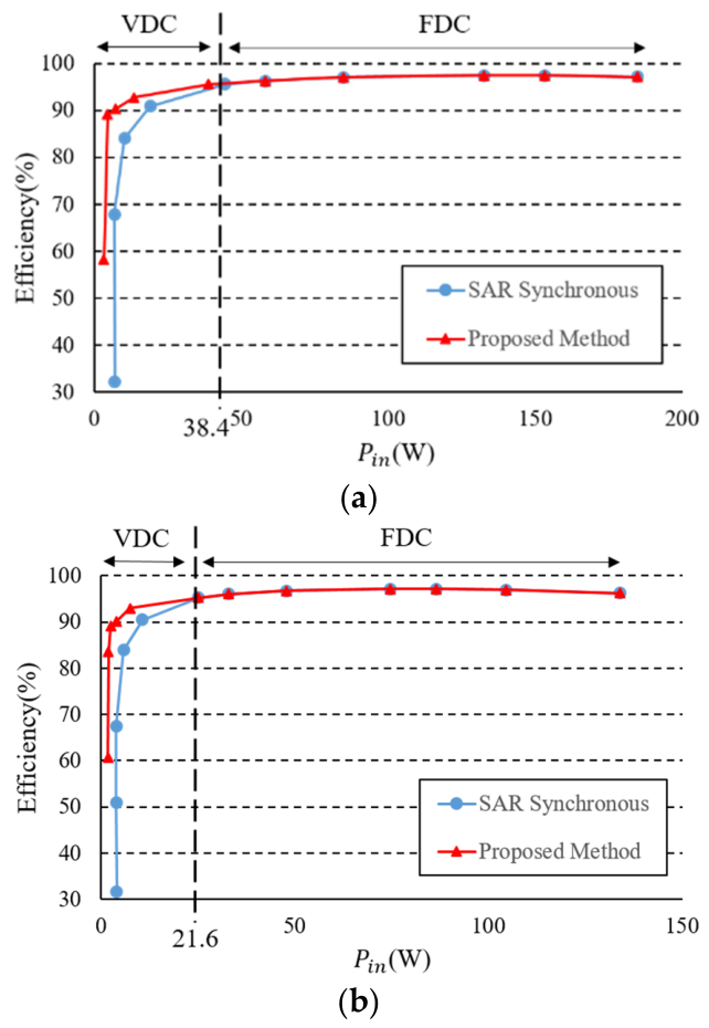
At the boundary condition, the efficiencies of the two control strategies become equal, indicating a transition between conduction-loss-dominant and switching-loss-dominant operating regions. This boundary can be interpreted as an equivalent load condition at which the dominant loss mechanisms of both control strategies are balanced and is therefore represented by a critical boundary resistance R b . To determine the control boundary between light and heavy loads, PSIM was used to evaluate the relationship between input power P i n and efficiency η for a half-bridge inverter under both fixed duty cycle and P&O control schemes, as shown in Figure 7. The simulation results show that the efficiency curves converge at P i n 38.4   W for V i n = 48   V and at P i n 21.6   W for V i n = 36   V , indicating that the boundary condition is consistently governed by an equivalent load behavior rather than a specific operating voltage.
Based on these observations, an empirical relationship between V i n and the critical input power P i n ( b o u n d ) is expressed as
P i n = V i n 2 R b
where R b represents the equivalent load resistance at the boundary condition. Consequently, R b = 60   Ω is obtained from simulation results and adopted as the practical criterion for switching between light-load and heavy-load control modes.
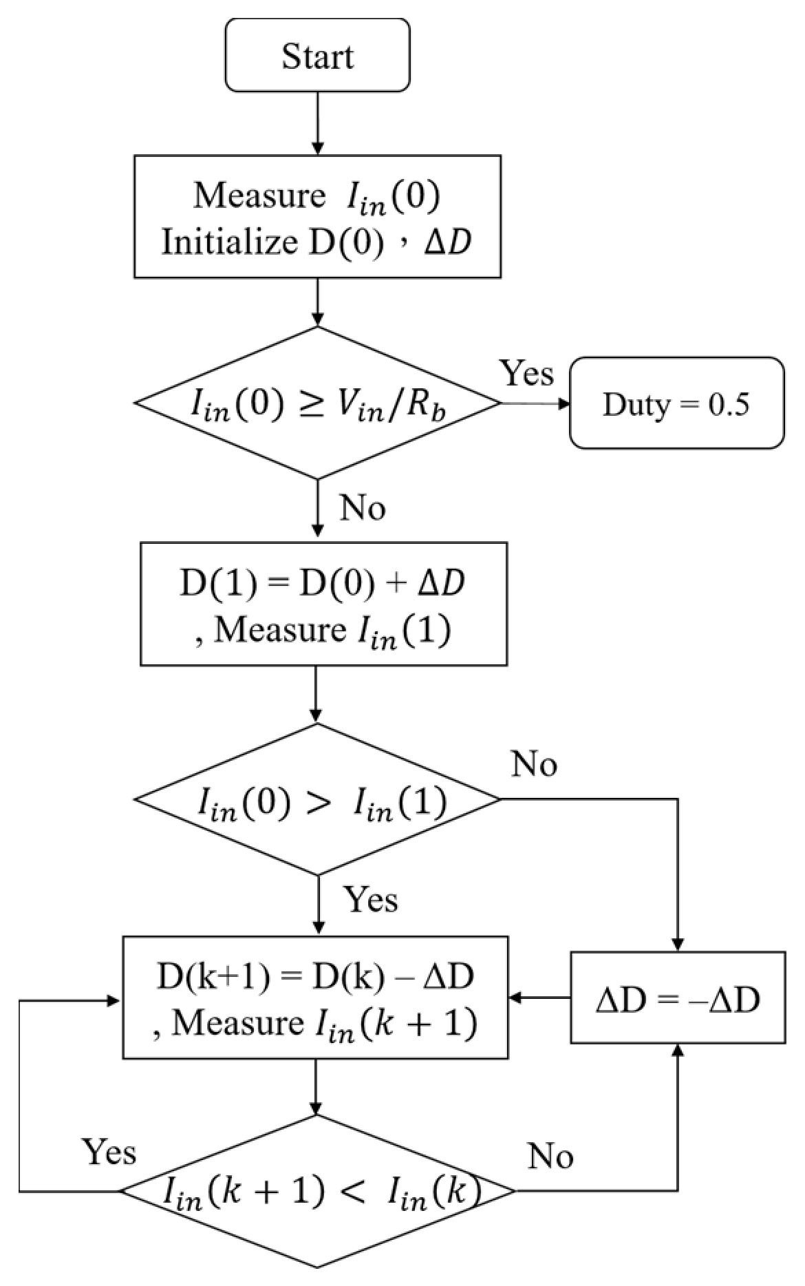
Figure 8 shows the control flowchart of the proposed system. The process begins by sensing the input current I i n k to determine the load state. In heavy-load mode, a fixed duty cycle of 0.5 is maintained. In light-load mode, the P&O control is implemented. The system first decrements the duty cycle by D of 0.01, with dynamic adjustments executed at an update frequency of 100 kHz. In the subsequent sampling period, the new input current I i n k + 1 is compared with I i n k . If I i n k + 1 < I i n k , it indicates that the system is still converging toward the minimum value, and the duty cycle continues to decrease by D . Conversely, if I i n k + 1 > I i n k , it signifies that the system has surpassed the minimum current point, and the duty cycle is then incremented by D to track the optimal operating point.

3.2. Control Strategy for Semi-Active Rectifier (SAR)

To reduce the system’s switching losses, this paper proposes a synchronous control method for the SAR. By implementing phase adjustment to synchronize switching signals with the voltage waveforms, the strategy ensures that the power switches achieve ZVS characteristics.
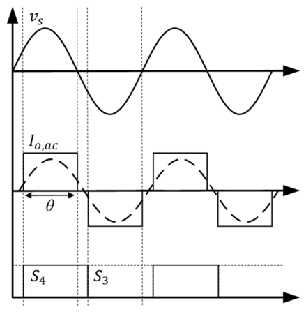
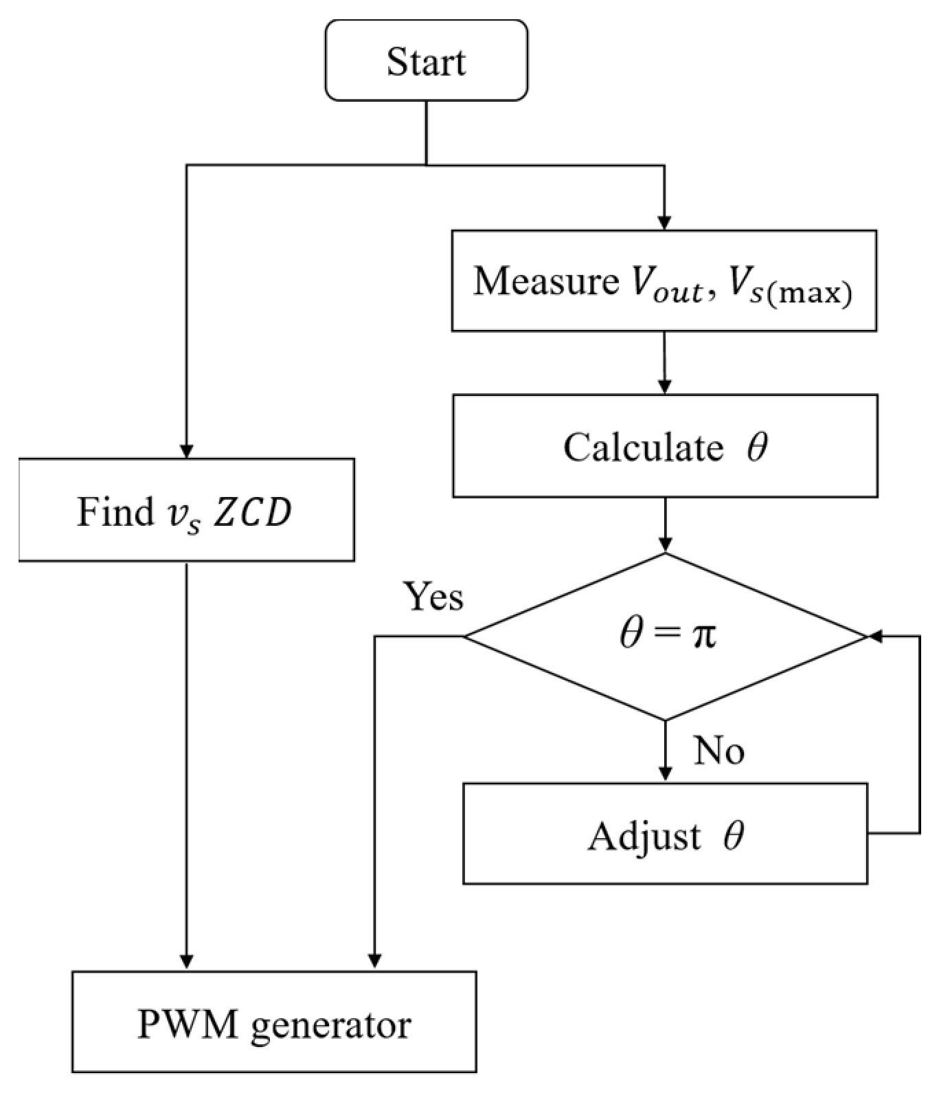
The operational waveforms are illustrated in Figure 9, while the flowchart of the specific control methodology is presented in Figure 10. The control procedure begins by sensing the secondary side AC voltage v s waveform and the output voltage v o u t , utilizing the zero-crossing point of v s as the synchronization reference. Any phase offset between the switching signals and v s is rectified in real time via phase-shift control. Based on fundamental harmonic analysis (FHA) as detailed in ref. [14], the relationship between the load voltage v o u t and the peak induced voltage v s ( m a x ) is defined as follows:
v s ( m a x ) = π 4 v o u t · c o s π θ 2
Substituting the measured v s ( m a x ) and v o u t into (42) allows the detection of phase offsets. If the resulting phase angle deviates from π , phase-shift control is employed to realign it. Such correction is essential to maintain ZPA and ZVS, which are critical for maximizing system efficiency.

4. Experimental Results

4.1. Experimental Hardware Prototype

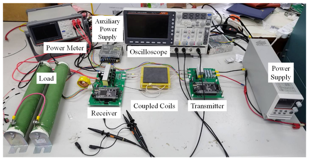
The experimental hardware prototype is depicted in Figure 11, which primarily consists of three parts: the wireless power transfer circuit, the driving circuit, and the control board. The control architecture is implemented using the TI TMS320F2833 DSP. Programming and compilation are performed via the Code Composer Studio v6.3 environment. This DSP precisely controls the MOSFETs within the half-bridge inverter and the SAR. The FDP054N10 MOSFET from Fairchild Semiconductor is employed as the switching element, while the STPS30M100S Schottky diode from STMicroelectronics is selected for the rectification circuit. Multilayer ceramic capacitors (MLCCs) are selected as the compensation elements.
The coupled coils are wound using Litz wire with a strand diameter of 0.1 mm and 450 strands to reduce skin and proximity effects at high frequency, thereby decreasing AC resistance and improving overall efficiency. A ferromagnetic sheet is placed above the coils, and the resulting parameter variations are summarized in Table 3. As shown in Table 3, the inclusion of the ferromagnetic sheet increases the inductances L p , L s , mutual inductance M , and coupling coefficient k , thereby strengthening magnetic flux linkage between the transmitter and receiver. This improvement is consistent with the analysis presented and contributes to enhanced power transfer efficiency. The output power was measured by a GW INSTEK GPM-8213 power meter.

4.2. Experimental Results of SP-WPT System

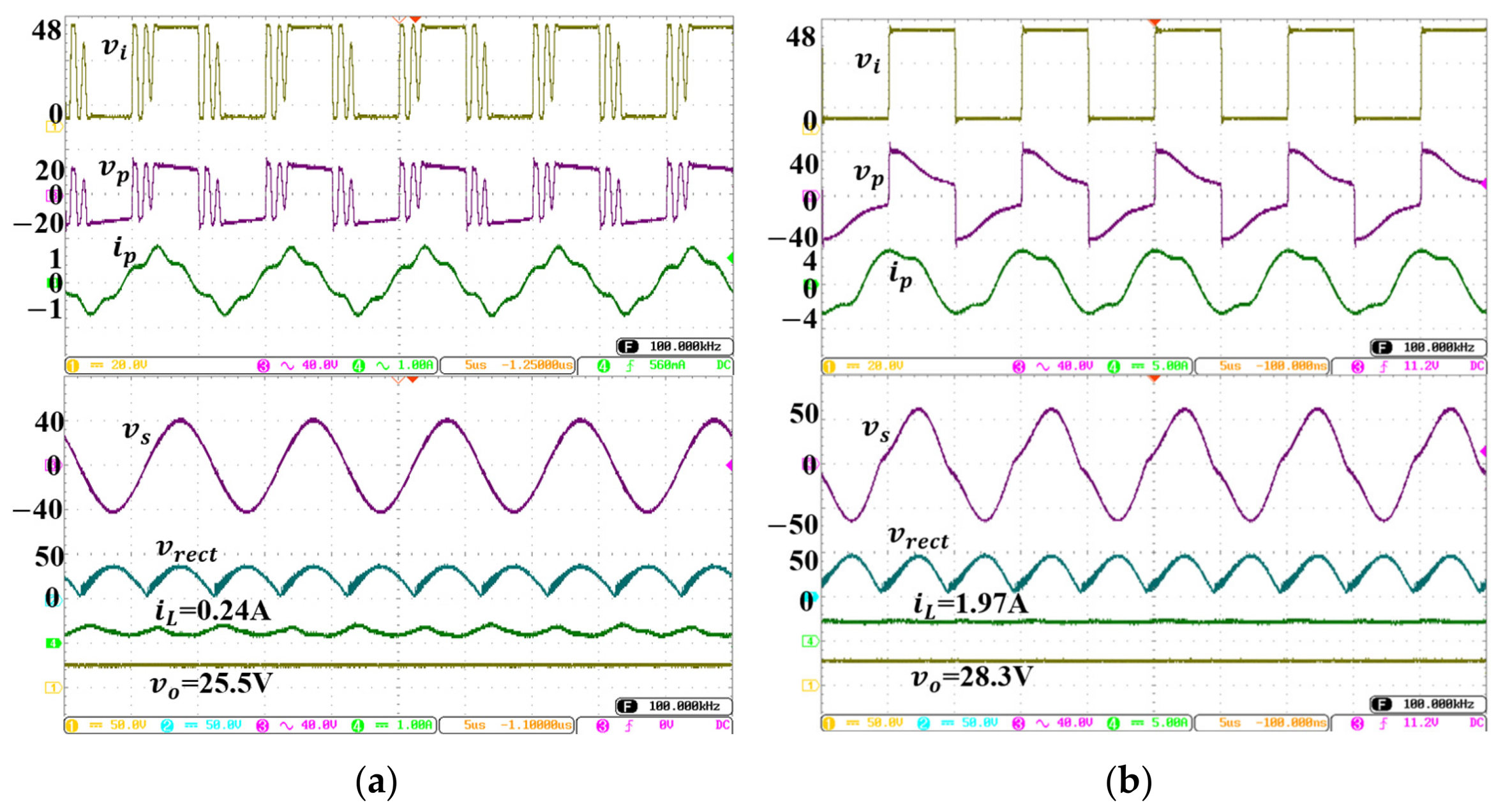
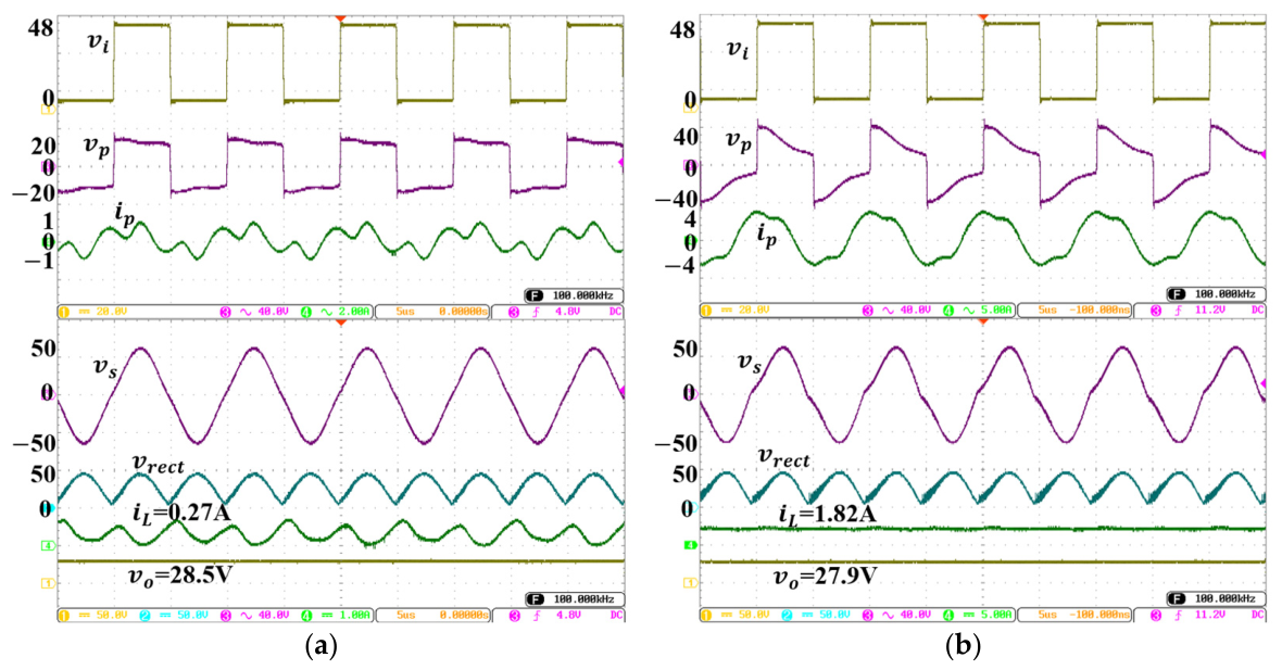
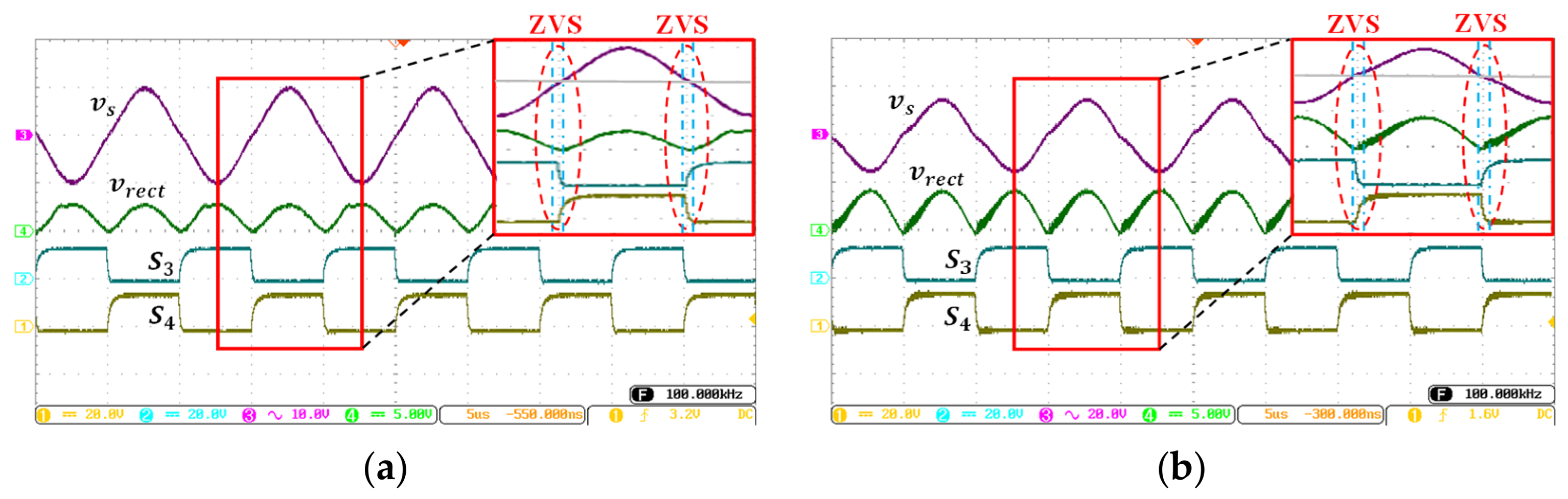
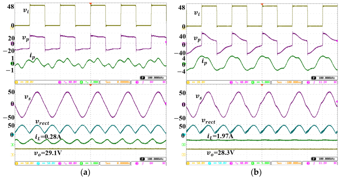
To validate the proposed method, circuit experiments were performed under three different conditions, with the results presented in Figure 12, Figure 13, Figure 14 and Figure 15. Comparing Figure 12 and Figure 14, it can be observed that both v o and i L of the SAR synchronous control system are higher than those of the diode rectification system. This indicates that the output efficiency of the SAR synchronous control is superior, which is attributed to its ability to achieve ZVS across all load conditions, as shown in Figure 13. Furthermore, although the v o and i L in Figure 15a are lower than those in Figure 14a, the reduction in input power driven by the v p drop from duty cycle adjustment leads to an overall improvement in system efficiency.
As shown in Figure 15a, the waveforms of v i and v p exhibit high-frequency ringing during switching transitions. This phenomenon is primarily attributed to the dead-time interval, where both half-bridge switches are briefly turned off. During this period, the inductive resonant current forces the body diodes to conduct, exciting a high-frequency parasitic resonant loop formed by the parasitic inductances and the device output capacitances. Since these oscillations are high-frequency transients that decay rapidly and constitute a very small fraction of the total switching period, their impact on overall system efficiency is negligible.
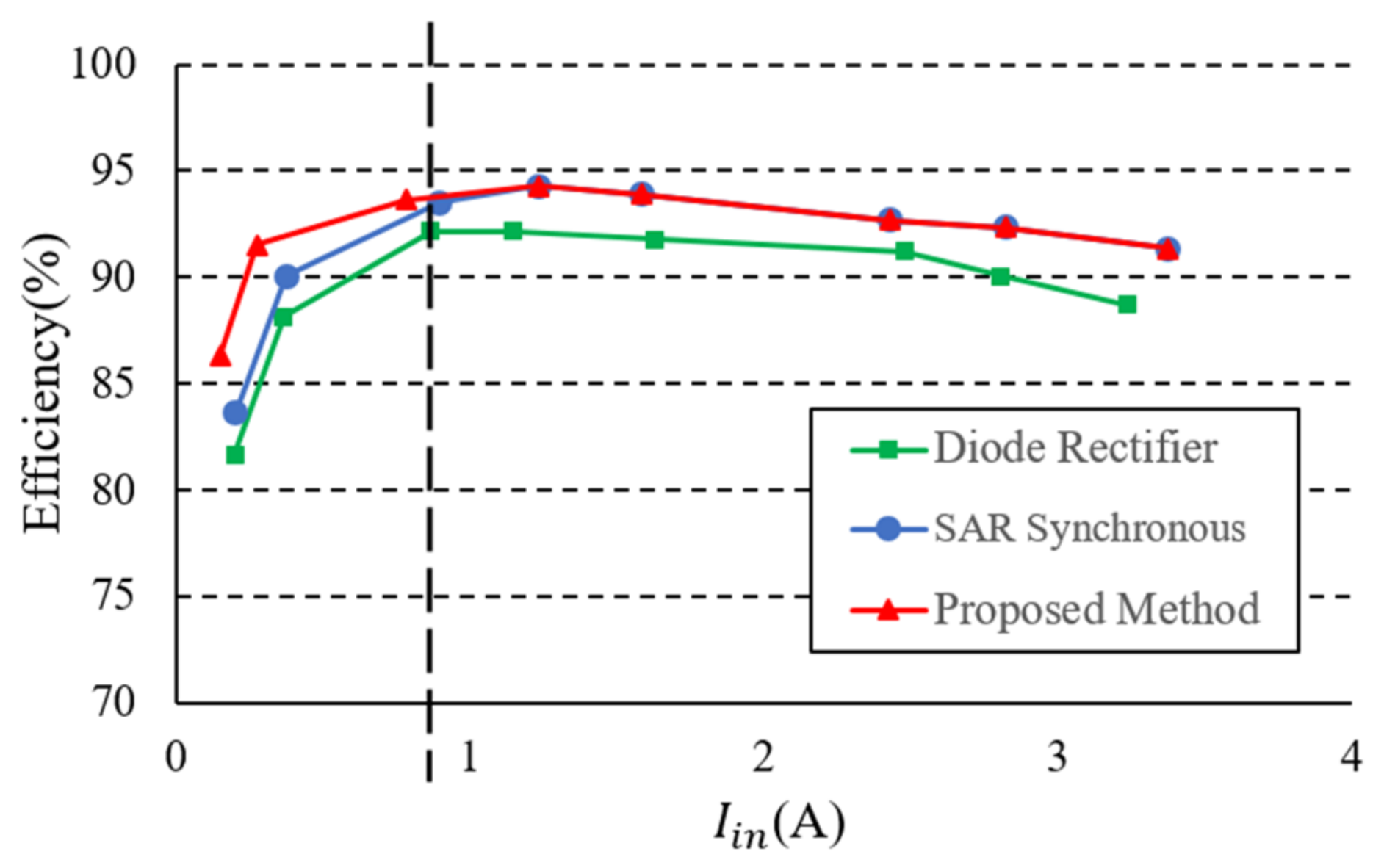
Figure 16 illustrates the relationship between input current I i n and efficiency η . The curves confirm that the proposed control method achieves the highest system efficiency, validating the effectiveness of this strategy in enhancing system performance. As illustrated by the results, the maximum efficiency occurs at a current of around 0.8 A. At this point, the load R L = 15   Ω , which is consistent with the theoretical optimal load R o p t calculated from (31).
The measured input power, output power, and efficiency for the three architectures under both light and heavy loads are presented in Table 4. At light loads, the proposed method significantly outperforms both diode rectification and SAR synchronous control. Under heavy-load conditions, the proposed control method demonstrates performance consistent with SAR synchronous control, with both considerably outperforming diode rectification. These experimental results validate the feasibility and advantages of the proposed methodology for practical applications.

4.3. Power Loss Analysis

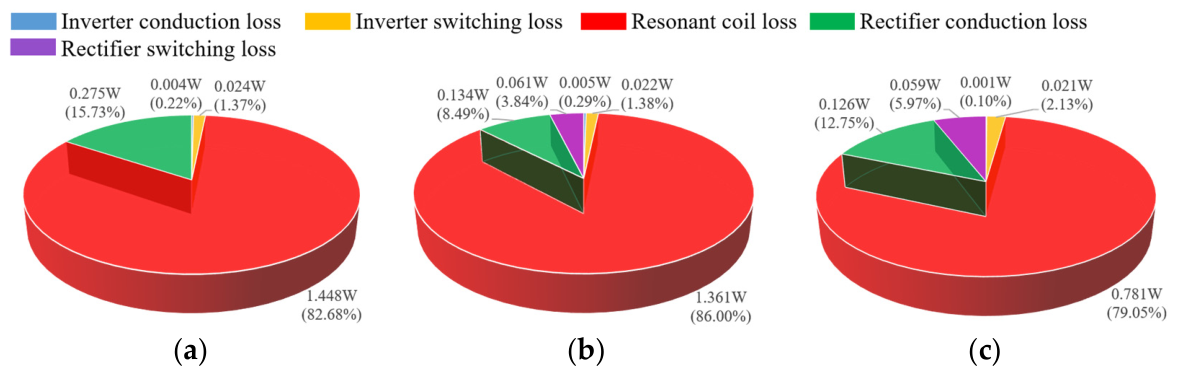
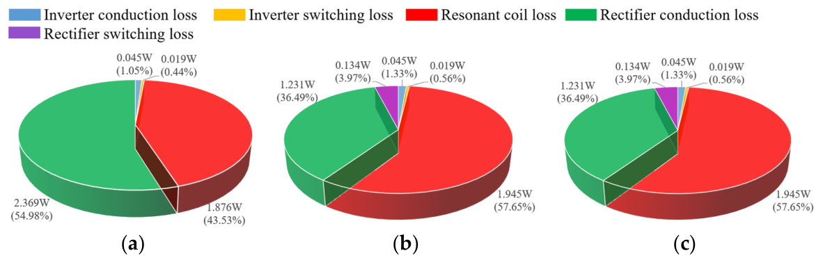
Figure 17 and Figure 18 present the power loss distributions under light-load ( R L = 100   Ω ) and heavy-load ( R L = 15   Ω ) conditions, respectively. As shown in Figure 17, under light-load conditions, the semi-active rectifier (SAR) with synchronous control achieves higher efficiency than conventional diode rectification. However, compared to the proposed strategy, the SAR synchronous control exhibits higher switching losses ( P s w ) and conduction losses ( P c o n ). This indicates that the proposed strategy effectively suppresses circulating currents under light-load conditions, thereby reducing switching losses and minimizing power dissipation in both the inverter and the SAR, thereby improving overall efficiency. Figure 18 illustrates the system performance under heavy-load conditions. Both the proposed strategy and the SAR synchronous control achieve lower rectifier losses than diode rectifiers. This improvement is attributed to the realization of zero voltage switching (ZVS) and zero phase angle (ZPA) characteristics, which effectively suppress the reactive power in the rectifier circuit. Consequently, the total power loss of the SAR synchronous control remains significantly lower than that of conventional diode rectifiers.

5. Conclusions

This paper proposes a control strategy for SP-compensated wireless power transfer systems to improve efficiency across the entire load range without increasing circuit complexity. By properly designing the resonant parameters to achieve zero phase angle (ZPA), the reactive power in the system is significantly reduced. On the secondary side, a SAR rectifier with synchronous control is employed to achieve zero voltage switching (ZVS), thereby reducing rectification losses. To address efficiency degradation under light-load conditions, a P&O-based variable duty cycle (VDC) control is integrated into the inverter to suppress circulating currents and enhance light-load performance. Under heavy-load conditions, the system seamlessly transitions to fixed duty cycle (FDC) control to maintain optimal operation. The proposed strategy not only improves efficiency but also enhances system stability during load transitions and reduces both reactive power and switching-related losses across different operating conditions. Experimental results validate the effectiveness of the proposed method. Compared with conventional diode rectification systems, the efficiency is improved by up to 4.61% under light-load conditions. In addition, a 2.6% efficiency improvement is achieved compared to SAR synchronous control systems, while maintaining stable and efficient operation across load variations.

Author Contributions

C.-Y.L. conceived the methodology, developed the algorithm, analyzed the results, supervised the research, and wrote and revised the manuscript; K.-Y.Q. designed the circuit, performed the experimental validation, and curated the data. All authors have read and agreed to the published version of the manuscript.

Funding

This research was funded by the National Science and Technology Council (NSTC) of Taiwan, under contract number NSTC 112-2221-E-239-020.

Data Availability Statement

Data are contained within the article.

Acknowledgments

The authors would like to thank the research project NSTC 112-2221-E-239-020 of National Science and Technology Council (NSTC), Taiwan for the support.

Conflicts of Interest

The authors declare no conflicts of interest.

References

  1. Zhang, Z.; Pang, H.; Georgiadis, A.; Cecati, C. Wireless Power Transfer—An Overview. IEEE Trans. Ind. Electron. 2019, 66, 1044–1058. [Google Scholar] [CrossRef] [Scilit]
  2. Nnamdi, U.C.; Asianuba, I.B. Wireless Power Transfer: A Review of Existing Technologies. Eur. J. Eng. Technol. Res. 2023, 8, 59–66. [Google Scholar] [CrossRef] [Scilit]
  3. Tamilselvi, M.; Durai, C.R.B.; Senthilkumar, B.; Latha, B.; Pandi, V.S.; Priya, J.L. WPT: A Smart Magnetic Resonance Technology based Wireless Power Transfer System Design for Charging Mobile Phones. In Proceedings of the 2024 International Conference on Intelligent and Innovative Technologies in Computing, Electrical and Electronics (IITCEE), Bengaluru, India, 24–25 January 2024. [Google Scholar]
  4. Bui, D.; Mostafa, T.M.; Hu, A.P.; Hattori, R. DC-DC Converter Based Impedance Matching for Maximum Power Transfer of CPT System with High Efficiency. In Proceedings of the 2018 IEEE PELS Workshop on Emerging Technologies: Wireless Power Transfer (Wow), Montreal, QC, Canada, 3–7 June 2018. [Google Scholar]
  5. Li, Z.; Huang, X.; Song, K.; Jiang, J.; Zhu, C.; Du, Z. Constant Current Charging and the Maximum System Efficiency Tracking for Wireless Charging Systems Employing Dual-side Control. In Proceedings of the 2018 International Power Electronics Conference (IPEC-Niigata 2018-ECCE Asia), Niigata, Japan, 20–24 May 2018. [Google Scholar]
  6. Bajelvand, S.; Jafari-Natanzi, A.; Varjani, A.Y.; Vaez-Zadeh, S.; Babaki, A. Design of Non-Communication Based WPT Battery Charging System With CP-CV Method. In Proceedings of the 2022 13th Power Electronics, Drive Systems, and Technologies Conference (PEDSTC), Tehran, Iran, 1–3 February 2022. [Google Scholar]
  7. Wang, X.; Zhang, X.; Wang, Y.; Ma, H.; Tian, J.; Li, R. Semi-Active Rectifier Based Single-Stage Wireless Battery Charging System with Dynamic Tuning Capability for Electric Vehicles. In Proceedings of the 2022 4th International Conference on Smart Power & Internet Energy Systems (SPIES), Beijing, China, 27–30 October 2022. [Google Scholar]
  8. Fu, N.; Deng, J.; Wang, Z.; Chen, D. Dual-Phase-Shift Control Strategy With Switch-Controlled Capacitor for Overall Efficiency Optimization in Wireless Power Transfer System. IEEE Trans. Veh. Technol. 2023, 72, 7304–7317. [Google Scholar] [CrossRef] [Scilit]
  9. Ding, Z.; Iam, I.W.; Ieong, C.F.; Lam, C.S. A Bivariate Control Strategy on Inductive Power Transfer Converter for Multi-Stage Constant Current Charging. In Proceedings of the IECON 2022—48th Annual Conference of the IEEE Industrial Electronics Society, Brussels, Belgium, 17–20 October 2022. [Google Scholar]
  10. Ann, S.; Byun, J.; Joo, D.; Lee, B.K. Integrated control of bridge type inductive power transfer systems for light load efficiency improvement. In Proceedings of the 2018 IEEE Applied Power Electronics Conference and Exposition (APEC), San Antonio, TX, USA, 4–8 March 2018. [Google Scholar]
  11. Zhu, G.; Dong, J.; Shi, W.; Soeiro, T.B.; Xu, J.; Bauer, P. A Mode-Switching-Based Phase Shift Control for Optimized Efficiency and Wide ZVS Operations in Wireless Power Transfer Systems. IEEE Trans. Power Electron. 2023, 38, 5561–5575. [Google Scholar] [CrossRef] [Scilit]
  12. Liu, S.; Mai, R.; Zhou, L.; Li, Y.; Hu, J.; He, Z. Dynamic Improvement of Inductive Power Transfer Systems With Maximum Energy Efficiency Tracking Using Model Predictive Control: Analysis and Experimental Verification. IEEE Trans. Power Electron. 2020, 35, 12752–12764. [Google Scholar] [CrossRef] [Scilit]
  13. Wu, M.; Jiang, Y.; Yu, L.; Yang, C.; Zhu, M.; Wang, J. A New Control Method of Semi-bridgeless Active Rectifier for Wireless Power Transfer System Based on the Double-sided LCC Compensation. In Proceedings of the 2020 IEEE Energy Conversion Congress and Exposition (ECCE), Detroit, MI, USA, 11–15 October 2020. [Google Scholar]
  14. Burye, R.; Figarado, S. A Novel Operation Scheme for a Series-Parallel compensated Inductive Power Transfer System for Coupling-Independent Compensation and Reduced Circulating Current. In Proceedings of the IECON 2023—49th Annual Conference of the IEEE Industrial Electronics Society, Singapore, 16–19 October 2023. [Google Scholar]
  15. Liu, H.; He, L.; Cheng, B. Powerless Fractional-Order Tuning Wireless Power Transfer System With Zero Phase Angle Input. IEEE Trans. Circuits Syst. I Regul. Pap. 2025, 72, 433–442. [Google Scholar] [CrossRef] [Scilit]
  16. Hao, Y.; Wang, J.; Liu, Y. Research on Wireless Power Transfer System of Automated Guided Vehicle Based on Magnetic Coupling Resonance. In Proceedings of the 2019 22nd International Conference on Electrical Machines and Systems (ICEMS), Harbin, China, 11–14 August 2019. [Google Scholar]
  17. Lu, C.Y.; Qiu, K.Y. Power Carrier-Based Simultaneous Wireless Power and Data Transfer Module for Photovoltaic Systems. IEEE Access 2025, 13, 157207–157219. [Google Scholar] [CrossRef] [Scilit]
  18. Zhang, Z.; Pang, H. Wireless Power Transfer—Principles and Applications; John Wiley&Sons: Toronto, ON, Canada, 2023. [Google Scholar]
  19. Imura, T. Wireless Power Transfer—Using Magnetic and Electric Resonance Coupling Techniques; Springer: Singapore, 2020. [Google Scholar]
  20. Li, Z.; Song, K.; Jiang, J.; Zhu, C. Constant Current Charging and Maximum Efficiency Tracking Control Scheme for Supercapacitor Wireless Charging. IEEE Trans. Power Electron. 2018, 33, 9088–9100. [Google Scholar] [CrossRef] [Scilit]
Figure 1. Proposed SP-compensated WPT system configuration.
Electronics 15 01908 g001
Figure 2. Equivalent circuit of proposed SP-compensated WPT system.
Electronics 15 01908 g002
Figure 3. Frequency response of input impedance Z i n .
Electronics 15 01908 g003
Figure 4. Frequency response of voltage transfer ratio G v .
Electronics 15 01908 g004
Figure 5. Equivalent circuit of proposed SP-compensated WPT system including coil internal resistance.
Electronics 15 01908 g005
Figure 6. Curves of input power and system efficiency with respect to duty cycle.
Electronics 15 01908 g006
Figure 7. The curves of system efficiency relative to input power. (a) V i n = 48   V , (b) V i n = 36   V .
Electronics 15 01908 g007
Figure 8. Flowchart of half-bridge inverter control strategy.
Electronics 15 01908 g008
Figure 9. Operating waveforms of the SAR.
Electronics 15 01908 g009
Figure 10. Flowchart of SAR control strategy.
Electronics 15 01908 g010
Figure 11. Hardware prototype and experimental setup.
Electronics 15 01908 g011
Figure 12. Experimental waveforms of diode rectifier ( V i n = 48   V ). (a) R L = 100   Ω ; (b) R L = 15   Ω .
Electronics 15 01908 g012
Figure 13. Experimental waveforms of ZVS achieved by the SAR ( V i n = 48   V ). (a) R L = 100   Ω ; (b) R L = 15   Ω .
Electronics 15 01908 g013
Figure 14. Experimental waveforms of SAR under synchronous control ( V i n = 48   V ). (a) R L = 100   Ω ; (b) R L = 15   Ω .
Electronics 15 01908 g014
Figure 15. Experimental waveforms of the proposed control strategy ( V i n = 48   V ). (a) R L = 100   Ω ; (b) R L = 15   Ω .
Electronics 15 01908 g015
Figure 16. Experimental curves of system efficiency versus input current for various control methods.
Electronics 15 01908 g016
Figure 17. System Power Loss for Light Load ( R L = 100 Ω ): (a) Diode rectifier. (b) SAR under synchronous control. (c) Proposed method.
Electronics 15 01908 g017
Figure 18. System Power Loss for Heavy Load ( R L = 15 Ω ): (a) Diode rectifier. (b) SAR under synchronous control. (c) Proposed method.
Electronics 15 01908 g018
Table 1. Comparison of Reported WPT Control Strategies.
Features[5][12][14]Proposed
Primary side topologyFull-bridge
inverter
Full-bridge
inverter
Full-bridge
inverter
Half-bridge
inverter
Secondary side topologySemi-active rectifierFull-bridge
rectifier
Semi-active rectifierSemi-active rectifier
Compensated
networks
SSSSSPSP
Number of
switches
6864
Number of
diodes
2042
Hardware costMediumHighMediumLow
Control
strategies
P&O control for buck converter, and phase-shift control for the SARP&O for inverter and MPC for SARInverter employs phase-shift control, and SAR switches operate with a turn-off delayP&O for inverter and phase shift for SAR
Computational complexityLowHighMediumLow
Operating range10~60 W72~578 W2~225 W6~200 W
Maximum
efficiency
82%93.8%93%94.3%
Table 2. Proposed SP-WPT Module Parameters.
ParameterValue
Resonant Frequency f o 100 kHz
Primary Coil Self-Inductance L p 11.99 μH
Secondary Coil Self-Inductance L s 13.5 μH
Mutual Inductance M8.67 μH
Coupling Coefficient k0.6815
Primary Side Capacitance C p 394.43 nF
Secondary Side Capacitor C s 187.63 nF
Primary Coil Resistance R p 13.5 mΩ
Secondary Coil Resistance R s 17.3 mΩ
Constant Voltage Gain G v 1.56
Filter Inductance L f 48.1 μH
Filter Capacitance C o 3000 μF
Table 3. Coil Parameters With and Without Ferromagnetic Sheets.
ParameterWithout
Ferromagnetic Sheet
With
Ferromagnetic Sheet
Primary Coil Self-Inductance L p 8.03 μH11.99 μH
Secondary Coil Self-Inductance L s 11.68 μH13.5 μH
Mutual Inductance M6.38 μH8.67 μH
Coupling Coefficient k0.65880.6815
Primary Coil Resistance R p 13.5 mΩ13.5 mΩ
Secondary Coil Resistance R s 17.3 mΩ17.3 mΩ
Table 4. Experimental System Power and Efficiency.
ParameterMethod P i n (W) P o u t (W) η (%)
R L = 100   Ω ,
V i n = 48   V
Diode rectifier9.557.8081.67
SAR under synchronous control9.708.1183.68
Proposed method7.106.4186.28
R L = 15   Ω ,
V i n = 48   V
Diode rectifier55.1050.7992.18
SAR under synchronous control59.1455.7694.29
Proposed method59.1455.7694.29
Disclaimer/Publisher’s Note: The statements, opinions and data contained in all publications are solely those of the individual author(s) and contributor(s) and not of MDPI and/or the editor(s). MDPI and/or the editor(s) disclaim responsibility for any injury to people or property resulting from any ideas, methods, instructions or products referred to in the content.