1. Introduction
Emerging artificial intelligence (AI) enabled next-generation wireless testbeds require custom compute architectures mapped to field programmable logic array (FPGA) fabrics. While radio frequency system-on-chip (RF-SoC) platforms, such as the Xilinx ZCU111 and ZCU1285, integrate high-speed data converters capable of multi-GS/s operation, their on-chip programmable logic resources are limited compared to large standalone FPGAs [
1,
2]. This motivates heterogeneous integration of multiple RF-SoCs with downstream FPGA accelerators that provide significantly greater logic capacity, thereby enabling complex digital signal processing (DSP) pipelines at the radio edge.
1.1. SerDes Technology and Multi-Gigabit Transceivers
Serializer/deserializer (SerDes) technology forms the foundation of high-speed interconnects in modern digital communication systems [
3]. As the demand for ever-higher throughput grows in both electrical and optical domains, advanced SerDes transceivers now deliver multi-gigabit-per-second (Gbps) data rates to support high-performance computing, cloud datacenters, and next-generation wireless communication networks [
4,
5,
6,
7,
8]. A SerDes architecture converts wide parallel data streams into high-speed serial bit streams for transmission over differential signaling links, such as low-voltage differential signaling (LVDS) or other high-speed physical layers. At the receiver, the data is deserialized into parallel form for subsequent DSP. This conversion reduces interconnect complexity and mitigates high-frequency signal integrity challenges, making SerDes a crucial technology for scalable and reliable high-speed communication links. In FPGA-based systems, multi-gigabit transceivers (MGTs) serve as the SerDes blocks capable of operating at data rates in the multi-gigabit range enabling board-to-board communication, high-speed memory access, and network interface connectivity [
3,
9,
10,
11,
12].
1.2. The Need for Scalable Compute Frameworks for Wireless Communication
Next-generation wireless systems including massive multiple-input multiple-output (MIMO) systems [
13,
14,
15,
16,
17], terahertz band communication links [
18,
19,
20,
21], integrated sensing and communications (ISAC) [
22,
23,
24,
25], and AI-native physical-layer signal processing [
26,
27,
28,
29] demand unprecedented computational throughput at the radio edge. These systems must process multi-gigahertz bandwidth streams from massive antenna arrays, resulting in high-dimensional spatio-temporal data that must be handled in real time. While both traditional and modern RF-SoC platforms provide significantly enhanced sampling rates (often operating in the multi-GS/s range), they remain constrained by the limited on-chip processing density for advanced signal processing and AI inference workloads [
30,
31,
32]. Therefore, scalable compute frameworks that partition workloads across heterogeneous devices are essential, with RF-SoCs responsible for high-speed direct-RF sampling, and downstream FPGA accelerators and graphics processing unit (GPU) clusters performing large-scale digital signal processing to satisfy real-time latency and throughput requirements.
1.3. Contribution of the Paper
This paper focuses on engineering design aspects for implementation of heterogeneous multi-FPGA systems, highlighting approaches to FPGA partitioning, high-speed streaming, and SerDes-based interconnects. We demonstrate two fully realized testbeds in which ZCU111 and ZCU1285 RF-SoC platforms (from AMD Xilinx, San Jose, CA, USA) are interconnected with Xilinx VCU128 and VCU129 FPGA accelerator boards (from AMD Xilinx, San Jose, CA, USA) over multiple 25 Gbps and 20 Gbps links, achieving maximum sustained real-time transfer rates of up to 50 Gbps per ADC–DAC channel. On the downstream VCU128/VCU129 platforms, FPGA-based MVM hardware cores are implemented using 8-phase polyphase decomposition, and the processed data are streamed back to the RF-SoCs for high-speed digital-to-analog converter (DAC) output. Additionally, we demonstrate system-level integration with an NVIDIA DGX Spark platform (from NVIDIA Corporation, Santa Clara, CA, USA), enabling higher-level AI/ML processing on the RF data as part of a scalable, AI-enabled wireless compute framework. The results showcase the potential of SerDes-enabled multi-FPGA frameworks as flexible, real-time DSP platforms for next-generation RF and AI-RF applications.
1.4. Organization of the Paper
The remainder of this paper is structured as follows.
Section 2 provides a comprehensive review of related work on multi-FPGA platforms, including large-scale cloud and datacenter-scale deployments, wireless communication and RF testbeds, and distributed AI accelerators.
Section 3 introduces the proposed scalable AI + DSP compute framework, discussing the theoretical background of the MVM core and the integration of the NVIDIA DGX Spark platform into the testbed. In
Section 4, we describe the digital design aspects of the realized prototype testbed in detail, covering the soft IPs utilized, the RF-SoC and FPGA platforms employed, the associated hardware and IP configurations, and the overall system-level dataflow architecture.
Section 5 presents the experimental setups and results for both configurations, including transmission coefficient measurements that demonstrate the practical viability of the testbed.
Section 6 provides a detailed discussion of the implementation challenges encountered during system realization, along with the practical workarounds adopted to address them. Finally,
Section 7 discusses the implications of the proposed architecture and outlines potential directions for future research.
2. Review
Recent advances in multi-FPGA platforms, particularly those interconnected through high-speed multi-gigabit transceivers, have enabled scalable and high-performance processing architectures that are increasingly essential for next-generation RF signal processing, wireless communication, and AI-accelerated systems. Prior work in this area can be broadly categorized into (i) cloud- and datacenter-scale FPGA deployments, (ii) multi-FPGA wireless communication and RF testbeds, and (iii) distributed FPGA accelerators for AI and signal processing. This section reviews representative efforts in each category and highlights the limitations that motivate the proposed scalable AI + DSP compute framework.
2.1. Cloud and Datacenter-Scale FPGA Platforms
Several notable efforts have demonstrated the deployment of reconfigurable logic at cloud and datacenter-scale. Microsoft’s Catapult project [
33,
34] integrates FPGAs directly into datacenter servers to accelerate large-scale workloads such as web search, machine learning inference, and network processing. The Catapult fabric interconnects Altera Stratix V D5 FPGAs in a
two-dimensional torus topology using custom lightweight serial links providing up to 20 Gbps bidirectional bandwidth over FMC and PCIe interfaces. Similarly, Amazon EC2 F2 instances [
35] deploy up to eight AMD Virtex UltraScale+ HBM VU47P FPGAs per node, interconnected via PCIe Gen3, enabling cloud based development and deployment of reconfigurable hardware accelerators. Furthermore, earlier large-scale efforts such as the Reconfigurable Computing Cluster (RCC) project [
36] explored petascale computing using network of Xilinx Virtex FPGAs interconnected through custom RocketIO MGT links operating at approximately 2.5 Gbps and employing Aurora 8B/10B protocol cores. While these platforms demonstrate impressive scalability, they primarily target cloud workloads and lack direct integration with high-speed RF data converters or real-time wireless signal processing pipelines.
2.2. Multi-FPGA Wireless Communication and RF Testbeds
In the context of wireless communication testbeds, several multi-FPGA platforms have been proposed to address scalability and real-time processing challenges. The FPGA-based digital wireless channel emulator [
37] distributes signal processing workloads across multiple interconnected Xilinx Virtex FPGA nodes to emulate large-scale wireless networks with up to 1250 devices at 1.9 MHz per-channel bandwidth. Inter-FPGA communication is achieved using GTX transceivers with 8B/10B encoding, providing 4 Gbps per lane. In a related effort, the authors in [
38] present a scalable clock-synchronization and data-communication framework for quantum-domain experiments, enabling deterministic clock distribution and fiber-based data transfer across multiple RF-SoC and FPGA boards. Their architecture relies on the Aurora 64B/66B protocol for high-speed optical communication, demonstrated using ZCU216 RF-SoC platforms. Similarly, Ref. [
39] introduces a modular multi-FPGA wireless MIMO-OFDM testbed based on CompactPCI hardware and interconnected Xilinx XC2V6000 FPGAs, enabling evaluation of spatial multiplexing and diversity techniques. While these platforms demonstrate distributed RF and baseband processing, they typically operate at relatively narrow bandwidths and do not explicitly address heterogeneous RF-SoC–FPGA partitioning for multi-gigahertz, AI-enabled wireless workloads.
2.3. Distributed FPGA Accelerators for AI and Signal Processing
Multi-FPGA acceleration has also been explored in the context of AI workloads. The authors in [
40] propose multi-chip convolutional neural network (CNN) accelerators that partition computation across several FPGA devices interconnected via the Aurora protocol, demonstrated on Xilinx ZCU102 and VU19P platforms. These works highlight the potential of FPGA clusters for scalable AI inference and training. However, they are not integrated with direct-RF data acquisition and real-time wireless signal processing.
In contrast to prior work, the proposed compute framework tightly integrates direct-RF RF-SoC platforms with high-capacity downstream FPGA accelerators using multi-lane 20–25 Gbps SerDes links, enabling sustained real-time data rates of up to 50 Gbps per ADC-DAC channel. Unlike cloud-centric FPGA clusters or narrowband wireless testbeds, this work focuses on multi-gigahertz bandwidth RF data streaming, hardware-partitioned DSP pipelines, and closed-loop RF processing, while also supporting system-level integration with GPU-based AI platforms such as NVIDIA DGX Spark, for higher-level learning and inference. Therefore, the proposed testbed bridges a critical gap between scalable multi-FPGA compute architectures and AI-native, real-time wireless experimentation.
3. Proposed Testbed Architecture
In this section, we present an overview of the proposed multi-FPGA DSP framework, including its distributed computation architecture, the implementation of the MVM core used for real-time digital signal processing, and integration of NVIDIA DGX Spark platform, which will be leveraged in future work to execute higher-level AI algorithms on the processed RF data.
3.1. Overview of the Proposed Scalable AI + DSP Compute Framework
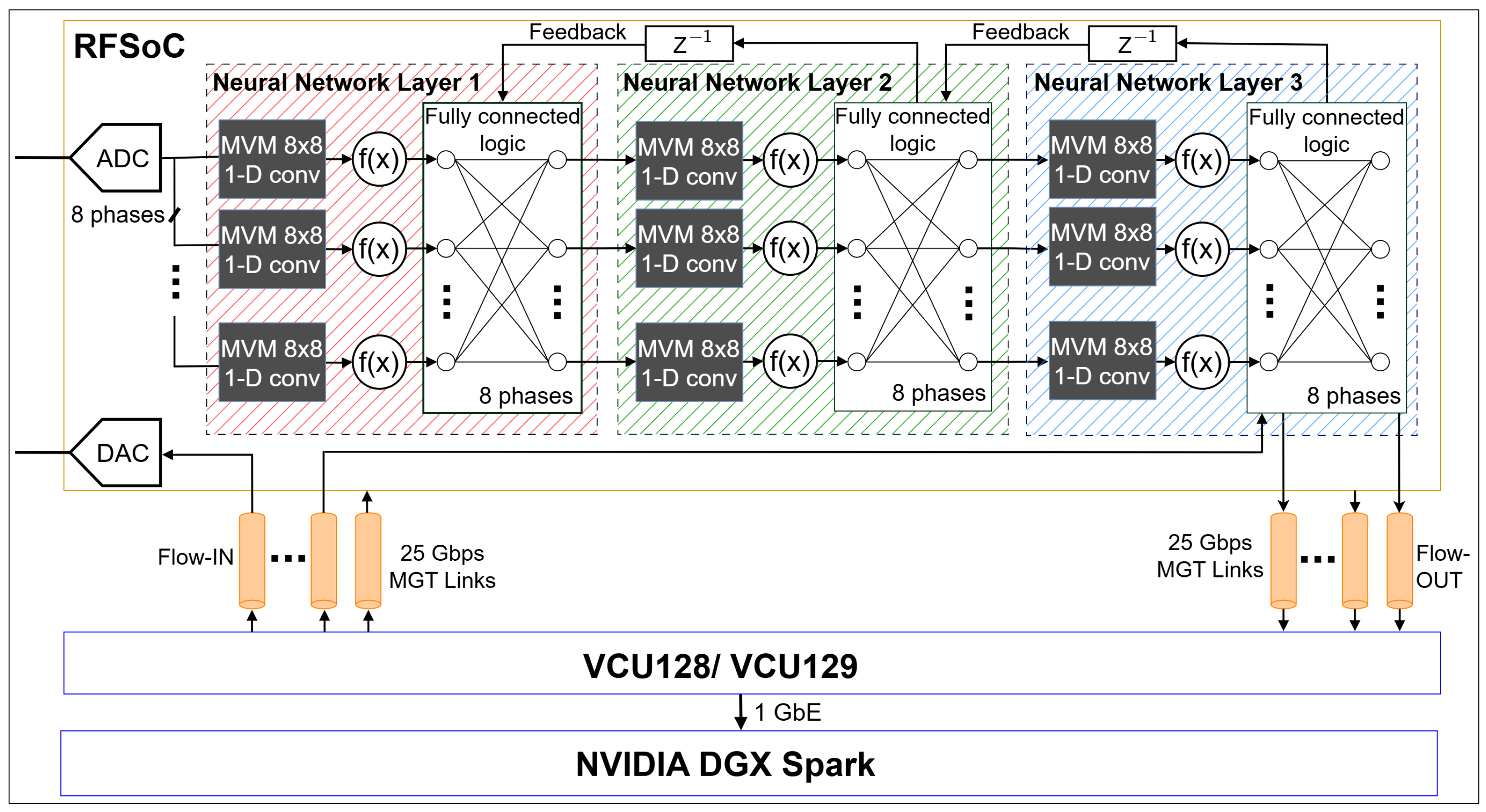
We envisage a scalable compute framework that leverages the heterogeneous integration of RF-SoCs and high-performance multi-FPGA platforms to enable AI-driven wireless testbeds. The proposed framework is illustrated in
Figure 1. In this architecture, the RF-SoCs perform direct RF data acquisition and transmission through their integrated data converters, while the compute-intensive DSP and AI workloads are transferred to downstream FPGAs with significantly greater logic, memory, and DSP resources. The high-speed direct RF sampling rates require the support for both massive parallelism and multi-rate signal processing using polyphase digital systolic arrays [
41]. The illustration depicts a subset of DSP and layers of a large multi-layer neural network implemented across multiple FPGA platforms in order to process the incoming polyphase ADC samples in training or inference. Due to the compute limitations in the RF-SoC, only a subset of the neural network layers is implemented, and the remaining layers are executed on the high-performance VCU128/VCU129 boards. Therefore, the output data of the RF-SoC implemented layers is transported through multiple 25 Gbps MGT links, which are realized across the selected FPGA platforms.
A single-layer implementation corresponds to multiple 8 × 8 MVM implementations. Each MVM core represents an 8 point convolution operation using 8 polyphase decomposition. Here, is the activation function, which is ReLU/Sigmoid, etc. Each activation outputs are fully connected with the nodes in the subsequent layer. Furthermore, during training stages, feedback information can be transferred to the preceding layers implemented on the upstream FPGA platforms through the same MGT links. Finally, the computed results can be routed back to the RF-SoC via the duplex MGT channels and output through the DAC, thereby enabling a closed-loop, real-time wireless testbed capability.
As an extension to the testbed, the DGX Spark platform is connected to the FPGA system via a 1 GbE interface to retrieve processed RF data for executing more advanced AI algorithms.
3.2. Matrix–Vector Multiplier (MVM) Core
The hardware realized MVM core is a fully parallel multiply–accumulate (MAC) engine tailored for high-speed RF/AI applications. It is built upon an 8 × 8 block of input samples together with an 8 × 1 weight vector and performs one length-8 dot product at each FPGA fabric clock cycle. Notably, it performs a real-time convolution operation,
where
denotes the convolution kernel used in AI/ML systems such as CNNs,
is a multi-GHz-rate wideband input signal, and
L is the length of the sequence
. This generic atomic unit can be realized on time-multiplexed or instantiated in parallel for higher-order matrix–vector operations, dense neural networks, and in polyphase finite impulse response (FIR) filters. In addition, the 8 × 8 MVM core can be used as a reconfigurable processing element (PE) in a tile-based AI + DSP compute fabric as proposed in this framework as illustrated in
Figure 1.
In order to achieve higher bandwidths, the MVM core is designed as a
M-phase polyphase architecture. Accordingly,
M parallel samples are produced per FPGA fabric clock cycle. If the FPGA clock index is
q,
for which
represents the effective high-rate sample index associated with the
q-th interleaved ADC and DAC paths. Accordingly, the
q-th output sample for each FPGA clock cycle
k is
In the prototype, the number of parallel phases is set to
and length of sequence
. To support the required 512 × 8 polyphase convolution operation, the architecture instantiates 64 parallel copies of the 8 × 8 MVM cores. This parallelization enables the system to compute all
M = 8 convolution outputs per FPGA clock cycle while sustaining the full
L = 512 tap processing requirement. The MVM architecture was designed using the Xilinx System Generator (SysGen) tool box in MATLAB R2020a [
42] to enable efficient development, verification, and seamless hardware realization. Once the design is simulated and verified, the complete MVM core was exported as a synthesizable SysGen IP. The generated SysGen IP was incorporated into the AMD Xilinx Vivado IP Integrator flow [
43] using Vivado v2020.2 to construct the complete digital system and interface with the remaining IP blocks in the design. This IP-centric workflow enables tight coupling between high-level DSP design and the low-level hardware infrastructure, ensuring efficient utilization of FPGA resources. As a result, the prototyped MVM core performs 4096 MACs/clock cycle in a single data path, resulting in real-time operations across 8 parallel data paths processing at 250 MHz on digital fabric, leading to 1 TeraMAC/s throughput. For detailed implementation specifics, the reader is referred to our prior work [
44].
3.3. Integration of NVIDIA DGX Spark Platform
The NVIDIA DGX Spark platform is introduced as a compact AI supercomputing solution aimed at individual developers, researchers, and students, addressing the traditional barrier of limited access to large-scale datacenter computation, which is implemented as a mini PC [
45]. It is based on the Grace Blackwell GB10 superchip, which combines an Arm-based Grace CPU and a Blackwell-class GPU within a single package. This tightly coupled CPU-GPU architecture enables high AI computation throughput up to the petaFLOP scale within a constrained power envelope, making it suitable for laboratory-scale deployment alongside FPGA-based RF systems. The system provides a 128 GB unified memory space shared between the CPU and GPU, which facilitates efficient handling of large datasets and model parameters during training and fine-tuning, while the network connectivity is provided through an integrated high-speed Ethernet interface, enabling consistent data exchange with the FPGA testbed.
In addition to high-speed data converters, Xilinx Zynq UltraScale+ RF-SoC platforms such as the ZCU111 and ZCU216 integrate embedded ARM Cortex-A53 cores, tightly coupled with programmable logic (PL) on a single chip. Using the PYNQ framework [
46,
47], the hardware is exposed through Python and Jupyter notebook interfaces, enabling researchers and designers to capture and process the acquired RF data in a flexible, software-driven environment. Within this experimental framework, the NVIDIA DGX Spark platform serves as a complementary “AI brain in the lab”, providing the heavy offline and near-real-time computational capability required for training neural receivers, channel models, synchronizer, and resource-allocation policies, as well as for conducting large-scale simulations, hyperparameter tuning, and architecture search on the acquired RF data using the PYNQ framework. The trained and optimized models can then be quantized and mapped back onto the multi-FPGA platform for inference, so that advanced AI-driven algorithms, developed using the computational power of DGX Spark, can be executed in real time over the air RF data on the proposed wireless testbed.
4. Digital Design Architecture
In this section, we discuss the digital design aspects of the realized multi-FPGA prototype testbed, detailing the soft IP cores employed in the system, as well as the hardware configuration of the RF-SoC and FPGA development boards. The overall platform is described in two architectural configurations: (i) an interconnected ZCU111-VCU128-VCU129 system linked through multiple 25 Gbps links, and (ii) an interconnected ZCU1285-VCU128 system operating over multiple 20 Gbps links. In addition, we outline the specialized cabling and hardware interfaces required to implement these high-speed connections in practice, which will help mitigate common challenges in digital-RF system integration for the broader research community.
4.1. A Starting Point to MGTs in Xilinx FPGAs
During our preliminary MGT configuration process, the Xilinx LogiCORE Integrated Bit Error Ratio Test (IBERT) IP for UltraScale/UltraScale+ GTY transceivers was employed to evaluate and monitor the high-speed serial links used in our system. This provides a reliable starting point for configuring MGT links. The IBERT core provides built-in pattern generators and checkers, enabling link verification through pseudo-random binary sequence (PRBS) testing and link status monitoring [
48]. We utilized this IP primarily to configure the PLLs, determine the correct clocking configurations, including reference clock sources and reference clock rates for a desired line rate, and to identify the specific GTY transceiver quads on each board for the targeted interfaces, following the XmYn naming convention where m and n represent its (x,y) coordinates of the transceiver location out of the available transceivers. Furthermore, the IBERT design aids hardware-level debugging and validation of GTY transceiver configurations by enabling eye diagram visualization and link status monitoring for established serial connections. This ensured valid transceiver configurations, facilitating reliable point-to-point and loopback connectivity across the multi-FPGA platform.
4.2. Aurora 64B/66B IP Core
To facilitate the implementation of multi-gigabit transceivers for Xilinx FPGAs, Xilinx has developed the Aurora 64B/66B protocol IP, offering a scalable, lightweight, link-layer protocol for high-speed serial communication. As its name suggests, the protocol employs 64B/66B encoding, which achieves very low transmission overhead and improves line efficiency. It supports data lanes with throughput ranging from 0.5 Gbps to 400 Gbps and is capable of both full-duplex and simplex configurations based on user requirements [
49]. The Aurora 64B/66B IP core supports the AXI4-Stream user interface, and its simple framing structure can be easily adapted to encapsulate user-specific data or even the data from other protocols, such as gigabit ethernet. Because of its low resource cost, scalable throughput, and flexible user interface, it is well-suited to chip-to-chip, board-to-board, and backplane links, as well as streaming applications [
49]. It is designed to automatically initialize and maintain channel integrity by transmitting idle sequences in the absence of user payload, thereby ensuring continuous link activity while reducing design complexity for system integration.
To implement the proposed architecture, we employed the ZCU111, ZCU1285, VCU128, and VCU129 FPGA platforms, each equipped with GTY transceivers. The Aurora 64B/66B IP core is used to leverage these transceiver lanes for data transport at the designated line rates. The core’s compatibility with AMD UltraScale+ and AMD Zynq device families enables seamless deployment across the selected platforms.
4.3. Multi-FPGA Prototype Testbed
We envision a scalable data processing pipeline that integrates multiple AMD Zynq UltraScale+ RF-SoCs with high-performance Xilinx FPGA platforms to serve as an emerging AI-native testbed.
The AMD Zynq UltraScale+ RF-SoC ZCU111 and ZCU1285 evaluation kits are employed as the primary RF data acquisition platforms in the proposed testbed. The ZCU111 provides eight 12-bit ADCs operating at up to 4.096 GSPS and eight 14-bit DACs at up to 6.554 GSPS, whereas the ZCU1285 extends this capability to sixteen ADC and DAC channels with comparable resolution but a reduced ADC sampling rate of 2.220 GSPS [
50,
51]. Despite the high RF sampling capability, the ZCU111 and ZCU1285 are constrained by relatively limited on-chip logic and DSP resources, with only 930 K system logic cells and 4272 DSP slices, which restrict their ability to implement complex AI-driven DSP workloads. To address this limitation, the acquired RF data is streamed to downstream FPGA platforms with substantially greater compute capacity. In particular, the AMD Virtex UltraScale+ VU37P FPGA on the VCU128 platform provides a significant increase in logic density, offering 2853 K system logic cells, 340.9 Mb of on-chip memory, and 9024 DSP slices, complemented by 8 GB of integrated high-bandwidth memory (HBM), thereby enabling efficient execution of compute-intensive DSP and matrix-based operations [
52]. This capability is further extended by the AMD Virtex UltraScale+ VU29P FPGA on the VCU129 platform, which delivers even greater compute capacity with 3780 K system logic cells, 454.5 Mb of on-chip memory, and 12,288 DSP slices, supporting deeper processing pipelines and larger-scale parallel architectures [
53]. Together, this heterogeneous architecture provides a flexible and scalable foundation for AI-native RF testbeds, where the RF-SoCs act as high-speed data acquisition front-ends and the VCU128/VCU129 platforms serve as powerful compute back-ends capable of sustaining real-time multi-gigabit dataflows.
4.4. Aurora 64B/66B IP Configuration
When working with the Aurora 64B/66B IP, proper IP configuration and the supporting logic are essential for the reliable establishment of MGT links across FPGA platforms. In our designs, the Aurora core manages GTY transceiver initialization, control character encoding and decoding, error detection, channel bonding, lane monitoring, AXI4-Stream data interfacing, and clock compensation, thereby ensuring reliable high-speed operation.
In each design, the Aurora IP was instantiated with GTY transceivers configured for the respective line rate and a lane count of four. To achieve the interested line rates of 25 Gbps and 20 Gbps, a GT reference clock of 156.25 MHz was used across all FPGA platforms, while the INIT_clk was configured at 250 MHz. Each channel was set in duplex mode with the framing interface enabled, and the supporting logic, including clocking and reset modules, was implemented following the guidelines of the provided example design of the Aurora 64B/66B IP.
In addition to these settings, the starting GT quad, GT lane parameter selection, and reference clock assignment should be carefully performed based on the target FPGA platform. A summary of such board-specific settings are shown in
Table 1 and
Table 2 based on the setup.
4.5. Hardware Configuration
The prototype testbed is realized in two distinct configurations, which are differentiated by their operating line rates of 25 Gbps and 20 Gbps. The corresponding system-level dataflow architectures for the interconnected ZCU111–VCU128–VCU129–DGX Spark platform and ZCU1285–VCU128 platform are illustrated in
Figure 2 and
Figure 3, respectively.
4.5.1. ZCU111–VCU128–VCU129 Platform: Interconnected at 25 Gbps
In this setup, two ADC/DAC pairs of the ZCU111 were configured with a sampling rate of 4.0 GSa/s. We employed a decimation/interpolation factor of 2, providing an effective instantaneous RF bandwidth of 1.0 GHz for each channel. The number of phases was set to 8, producing a 128-bit output word from each ADC at a 250 MHz FPGA fabric clock. These two 128-bit words, corresponding to the outputs of the two ADC channels, were repacked into a single 256-bit word. This aggregated data stream was then passed to a custom frame generator module, which generated the _tlast and _tkeep signals to define frame boundaries and formatted the output bus to comply with the AXI4-Stream protocol required by the Aurora IP. Based on the target line rate of 25 Gbps, the user logic interfacing with the Aurora core must operate at a clock frequency of 390.625 MHz. Therefore, an asynchronous first-in–first-out (FIFO) buffer configured in packet mode was employed to manage the clock domain crossing (CDC), with three CDC synchronization stages to ensure reliable data transfer. With the Aurora IP configured in a four-lane full-duplex architecture, where each lane operates at 25 Gbps, the interface achieves a combined throughput of 256 bits at 390.625 MHz, corresponding to an effective bit rate of 100 Gbps (i.e., 4 × 25 Gbps across the four lanes).
The sample data captured from the ZCU111 was then transmitted through its SFP28 interface using a 0.5 m Cisco QSFP-4SFP25G-CU50CM-compatible breakout cable (100G QSFP28 to 4 × 25G SFP28 passive direct-attach copper cables from FS.com Inc., New Castle, DE, USA), and it was received at the QSFP28 interface of the VCU128. The VCU128 design comprised two Aurora IP instances to facilitate connectivity with both ZCU111 and VCU129 platforms. In this configuration, the first Aurora instance received the incoming data, which was subsequently passed through to the second Aurora instance for transmission. Since the user_clk signals for the two Aurora instances were generated from independent clock sources, asynchronous FIFOs were inserted between them to ensure reliable duplex operation across the channel.
From the VCU128, the data was further transmitted to the VCU129 board via a similar QSFP28-to-SFP28 breakout cable connected to the SFP28 interface bank. On the VCU129, the AXI4-Stream data bus was routed to the DSP logic (referred to here as MVM cores) and its output is connected to the transmit interface of the Aurora IP instance, enabling the data to traverse the same boards in the reverse direction and return to the ZCU111 RF-SoC for DAC reconstruction.
In addition, the NVIDIA DGX Spark platform communicates with the ZCU111 over high-speed Ethernet using standard networking protocols (e.g., UDP/TCP sockets) through PYNQ framework to exchange RF data and control information, thereby enhancing the overall capability and flexibility of the testbed.
4.5.2. ZCU1285–VCU128 Platform: Interconnected at 20 Gbps
This setup exploits the GTY transceivers available in the ZCU-1285 RF-SoC interfacing through Samtec Bullseye connectors (Samtec RSP-200723-02-BEYE cable assembly from Samtec Inc., New Albany, IN, USA). On the VCU128 side, an 8-port SMA/34-pair LVDS FPGA Mezzanine Connector (FMC) daughter card (from HiTech Global, LLC, San Jose, CA, USA) is employed, connected through the FPGA Mezzanine card plus high serial pin count (FMCP HSCP) connector interface, which provides access to 8 serial transceivers, with the SMA cables from the RF-SoC connected to this module.
From the RF data converter side, two ADC/DAC pairs were configured with a sampling rate of 2.0 GSa/S with an effective instantaneous RF bandwidth of 1.0 GHz for each channel. The line rate was set to 20 Gbps, as the 25 Gbps configuration resulted in insufficient eye opening with the existing physical connections. As a result, the core operation frequency is 312.5 MHz. With the Aurora IP configured in a four-lane full-duplex architecture, where each lane operates at 20 Gbps, the interface achieves a combined throughput of 256 bits at 312.5 MHz, corresponding to an effective bit rate of 80 Gbps. The digital design components used in this configuration were similar to those in the previous setup, including bit combiners/splitters, frame generators, and FIFO buffers. The captured RF data are transported to the VCU128 FPGA and fed to the MVM cores, after which the resulting output is returned to the ZCU1285 and transmitted through the DAC.
5. Experiment Setup and Results
Figure 4 compares the measured eye diagrams obtained using the IBERT eye scan utility under different physical interconnects and line rates. As shown in
Figure 4a, the 25 Gbps Bullsye-to-FMC connection shows a severely constrained eye opening, with an open-UI of 0%, indicating insufficient timing margin for reliable operation at this line rate. In contrast, reducing the line rate to 20 Gbps for the same Byllsye-to-FMC path, as shown in
Figure 4b, significantly improves the signal integrity showing an open-UI of 44.44% and a comparatively larger open area, enabling stable link operation.
Figure 4c demonstrates that for the SFP28 based interconnect, the 25 Gbps configuration achieves a considerably wider eye opening with an open-UI of 55.56%, confirming that the SFP28 based physical channel provides better signal integrity than Bullseye-to-FMC interconnect. These measurements further validate that the Bullseye-to-FMC path is the primary limiting factor at higher line rates, thereby motivating the use of reduced line rate of 20 Gbps for the ZCU1285–VCU128 platform for robust and reliable operation.
Figure 5a presents the experimental setup of the ZCU111–VCU128–VCU129 platform interconnected via QSFP28-to-4×SFP28 breakout cables, with the DGX Spark connected through a 1-GbE link. For demonstration, the 512-tap MVM core, configured as a bandpass filter, is implemented on VCU-129 FPGA, with a single ADC sample data stream routed through the entire testbed. The demonstrated bandpass filter’s impulse response
is designed using Equation (
3).
The transmission coefficient (
) between the ADC and DAC ports was measured using an Agilent FieldFox N9923A (6 GHz) RF vector network analyzer (from Agilent Technologies, Santa Clara, CA, USA) calibrated up to 1 GHz with 10,001 points. Furthermore, the DGX Spark unit is connected to the ZCU111 with 1 GbE connection as illustrated.
Figure 6a shows the normalized
magnitude response of the implemented bandpass filter. The result illustrates a sharply defined passband over the 320–360 MHz frequency range and strong attenuation across the stopband.
Figure 5b depicts the corresponding setup for the ZCU1285–VCU128 platform where the MVM core configured as a moving average low-pass filter is implemented on VCU128. The low-pass filter is implemented with
using the 512-tap MVM core.
Figure 6b shows the resulting normalized
magnitude response of the entire setup. Both measured responses exhibit close alignment with the MATLAB-simulated theoretical response across the full 1 GHz bandwidth. These results collectively confirm the correct operation and practical feasibility of the proposed scalable AI + DSP compute framework across the full RF bandwidth.
In addition, system-level integration of the DGX Spark platform with the proposed testbed was experimentally validated by transferring captured RF samples from the ZCU111 to the DGX Spark unit via the PYNQ framework. This integration confirms the feasibility of extending the testbed toward an AI-native architecture capable of supporting higher-level learning and inference on captured and processed RF data. While this work establishes the end-to-end dataflow and system integration, comprehensive evaluation of advanced learning and inference algorithms on the DGX Spark platform is reserved for future work.
6. Implementation Challenges and Practical Workarounds
The realization of this scalable, multi-FPGA AI + DSP computational framework using RF-SoC and high-performance FPGA platforms presents several nontrivial engineering challenges. This section discusses the key implementation issues encountered during system development, along with the solutions and workarounds adopted. These insights are intended to aid practitioners in reproducing and extending similar high-speed, SerDes-enabled RF systems.
6.1. Identification of Correct MGT Interfaces and GTY Quad Selection
A fundamental challenge during implementation was the correct identification of the MGT interfaces and their corresponding GTY quads for each FPGA platform. Each physical connector (i.e., SFP28, QSFP28, FMC, and Bullseye) maps to specific GTY transceiver locations following the Xilinx XmYn naming convention. Based on this convention, accurate selection of the starting GT quad and lane is essential for successful Aurora IP configuration. This required careful cross-referencing of FPGA evaluation board user guides [
50,
51,
52,
53] and its schematic documents provided on the Xilinx product pages. To validate the correctness of the selected interfaces, the IBERT example design [
54] was extensively used. IBERT enabled verification of link establishment through lane and channel status indicators and facilitated confirmation of the correct XmYn mappings for the target interfaces. To assist readers in reproducing the design,
Table 1 and
Table 2 under
Section 4.4 list the connector interfaces, corresponding GTY quads, and starting lane selections for each RF-SoC and FPGA platform employed in this testbed.
6.2. Clocking Configuration
Selecting appropriate clocking configurations is one of the most critical aspects for stable operation of the Aurora 64B/66B IP at the target line rates. Two primary clock domains must be correctly defined: the GT reference clock and the system clock (INIT_clk).
For the evaluated line rates of 25 Gbps and 20 Gbps, a GT reference clock frequency of 156.25 MHz was selected across all platforms. This choice was motivated by three factors: (i) it is the default reference clock supported by the GTY transceivers on the evaluated boards, (ii) the required clock files are readily available through the system controller resources provided by the vendors, and (iii) the same reference clock configuration is recommended in IBERT reference designs for reliable high-speed operation. The specific GT reference clock sources used for each platform are listed in
Table 1 and
Table 2 (
Section 4.4).
The Aurora core additionally requires a free-running system clock (
INIT_clk) for its initialization which can be sourced either from a dedicated FPGA fabric clock pin or from a reference clock input associated with one of the GTY transceivers. In this work, a 250 MHz
INIT_clk was used, which consistently resulted in reliable lane initialization and channel bring-up. In cases where sufficient FPGA fabric clock pins were unavailable (specifically on the VCU128 platform), unused transceiver reference clocks were reused as the free-running system clocks. These clocks cannot be directly connected to fabric logic and must instead be routed through appropriate
IBUFDS_GTE* primitives and constrained correctly in the Xilinx Design Constraints (XDC) file, as described in Ref. [
55].
6.3. AXI4-Stream-Compliant RTL Modules
Another significant challenge involved ensuring correct AXI4-Stream protocol [
56] compliance across custom digital modules used in the data path, including frame generators, and MVM core modules. Reliable inter-FPGA RF data transport requires strict adherence to AXI4-Stream protocol, particularly the correct alignment and timing of
_tvalid,
_tdata,
_tkeep, and
_tlast signals. Early design issues were addressed by updating the custom modules to ensure that the
_tvalid signal was asserted only alongside valid data and by introducing packet-aware buffering using FIFOs configured in packet mode. These changes were essential for achieving stable, continuous data streaming across multiple FPGA devices at multi-gigabit rates.
6.4. Handling Non-Sequential GTY Lane Connectivity on QSFP28 Interfaces on VCU129
An additional practical consideration arose when configuring the Aurora 64B/66B IP on the VCU129 platform using QSFP28 interfaces. The QSFP28 connector maps to multiple GTY quads (Quads 124–127); however, within each quad, only a subset of the GTY lanes are physically connected. For instance, in Quad 124, only GTY0 and GTY2 are routed to the connector, while GTY1 and GTY3 are unconnected.
This non-sequential lane connectivity complicates GUI-based Aurora IP configuration, which typically assumes contiguous lane assignments. To address this limitation, explicit lane selection was performed during I/O planning, ensuring that only physically connected GTY lanes were enabled in the Aurora configuration. This approach is documented in the Xilinx I/O planning guidelines [
57,
58] and enabled successful 128-bit data transmission using multiple non-contiguous lanes within the same quad.
7. Discussion
Emerging AI-driven RF systems demand increasingly complex computational tasks, requiring scalable and efficient DSP frameworks. In this work, we present a scalable DSP compute framework tailored for AI-native RF testbeds by leveraging interconnected Xilinx multiple FPGA platforms through multi-gigabit transceiver links. We validated the implementation of the platform through two experimental setups. The ZCU111–VCU128–VCU129 platform achieves a combined throughput of 100 Gbps, corresponding to 50 Gbps per ADC stream, whereas the ZCU1285-VCU128 platform provides a slightly lower combined throughput of 80 Gbps, corresponding to 40 Gbps per ADC stream. Integrating both these configurations yields a fully interconnected, all-to-all wireless testbed that enables rapid prototyping of real-time wireless communication systems and beyond-5G/6G baseband pipelines, including higher-order modulation and demodulation schemes, polyphase filtering, real-time spectrum sensing, beamforming, and MIMO testbeds, as well as AI-assisted PHY and MAC-layer algorithms tightly coupled to high-speed RF front-ends. The experimental validation using real-time transfer function measurements across 1 GHz of instantaneous RF bandwidth, combined with the implementation of the MVM core on high-performance FPGA platforms, further demonstrates the viability of the proposed AI + DSP computing testbed for broader scientific, commercial, space, and defense applications. Moreover, the integration with the NVIDIA DGX Spark platform provides a path toward executing higher-level AI algorithms on the RF data processed by the multi-FPGA system, enhancing its capability as a next-generation AI-enabled wireless research testbed.
Compared to prior multi-FPGA and wireless testbeds, the proposed system uniquely combines direct-RF RF-SoC front-ends with high-capacity downstream FPGA accelerators and GPU-based AI platforms using sustained multi-lane 20–25 Gbps SerDes links, enabling real-time processing of multi-gigahertz RF bandwidths that exceed the capabilities of existing implementations. Current limitations arise primarily from physical interconnect constraints at the highest line rates, specifically with the ZCU1285-VCU128 platform, while full-scale AI learning evaluations are reserved for future work.
The authors plan to expand the platform by interconnecting a ZCU216 RF-SoC evaluation kit and a Stratix-10 AX FPGA development kit to support wider-band, higher-channel-count heterogeneous RF acquisition. This expanded architecture will enable the generation of advanced, high-fidelity RF datasets that will be highly valuable to the AI-enabled wireless research community.


