1. Introduction
In the ever-evolving landscape of computational technology, the pursuit of optimal performance and efficiency has propelled the exploration of groundbreaking paradigms. At present, the traditional von Neumann architecture has gradually failed to meet the requirements. In the von Neumann architecture, the storage and processing of data are separated, and the data is transmitted between the memory and the processor, which has several disadvantages. First of all, the access speed of the memory is far less than the processing speed of the processor, so the overall computing speed of the system will be limited by bandwidth, resulting in the actual computing power of the processor being far lower than the theoretical computing power. It is difficult to meet the needs of fast computing of intelligent chips; this problem is called the “memory wall” problem. By increasing the bandwidth and clock frequency, the performance of the processor can be improved to a certain extent, but at the same time, this will lead to large power consumption and integration costs, so its scalability is seriously limited. Secondly, in the von Neumann architecture, the storage and processing of data are separated, and the data are frequently transferred between the storage module and the computing module, which generates huge transmission power consumption; this is also known as the “power wall” problem [
1,
2,
3,
4]. For example, Nvidia research reports that floating-point operations require about 200 times more data transfer power than data processing power [
5]. These “memory wall” and “power wall” problems have become major bottlenecks of conventional von Neumann architectures. Therefore, the evolution of in-memory computing has emerged as a transformative force, reshaping traditional approaches to data processing. In-memory computing diverges from conventional architectures by executing computations directly within the storage medium, eliminating the need for frequent data transfers between storage and processing cells.
A variety of computing-in-memory (CiM) architectures with different storage media have been proposed here. In 2019, Static Random-Access Memory (SRAM)-based CiM architectures were proposed, which can realize the convolutional operation of neural networks with binary weights [
6]. In 2020, there have been proposed a CiM chip based on Resistive Random-Access Memory (RRAM), which can greatly improve computing power while reducing computing delay [
7]. In 2021, some scholars proposed a Dynamic Random-Access Memory (DRAM) CiM architecture, which can realize the acceleration of neural networks [
8]. Moreover, several different in-memory computing architectures have been reported recently, such as in-memory computing architectures based on SRAM, DRAM, Flash, RRAM, Phase Change Memory (PCM), Ferroelectric Field Effect Transistor (FeFET), and Magnetoresistive Random-Access Memory (MRAM) [
9,
10,
11,
12,
13,
14,
15,
16,
17,
18,
19,
20,
21,
22,
23,
24,
25,
26,
27,
28,
29,
30].
As a storage cell for CiM applications, Ferroelectric Random-Access Memory (FRAM) based on ferroelectric capacitors has advantages over other storage media. Compared to DRAM and SRAM, ferroelectric memory is non-volatile memory with the ability to preserve data in the event of power failure, which facilitates low-power design. Compared with DRAM, FRAM has better reliability for computing-in-memory. FRAM has lower read and write power consumption than MRAM, Flash, and PCM, which is consistent with the low power consumption requirements of computing-in-memory. FRAM has faster read and write speed than Flash and PCM, which has the potential to increase the speed of CiM accelerators. Compared with FeFET, FRAM has a mature process, which is more conducive to the formation of mature products. FRAM based on Hf
0.5Zr
0.5O
2 has the advantages of high compatibility with CMOS technology [
31,
32,
33,
34,
35,
36,
37,
38,
39,
40].
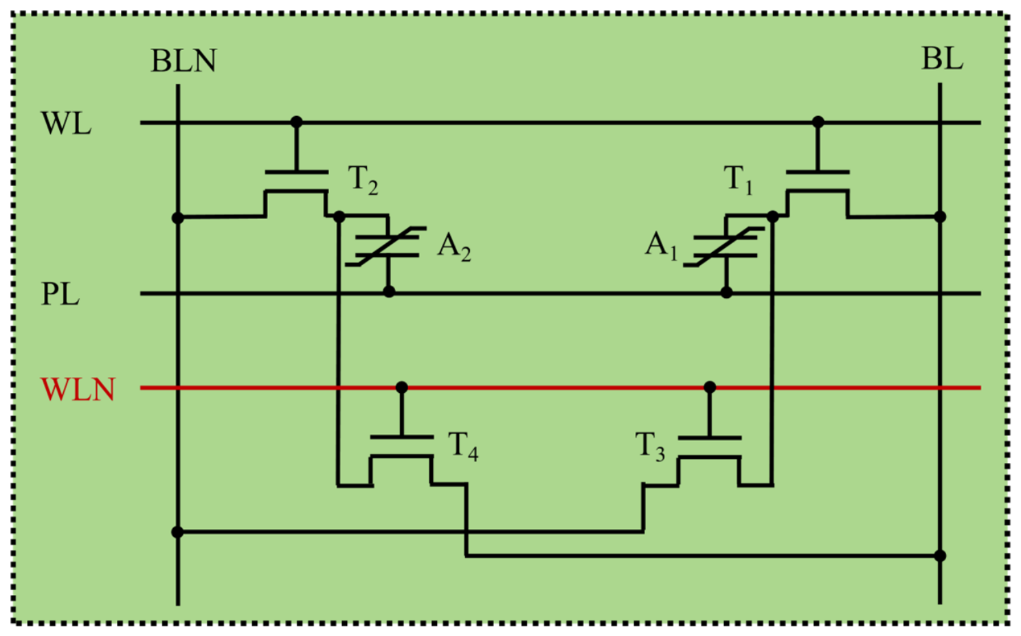
In this work, we propose a bitwise in-memory computing architecture based on 2T-2C and 4T-2C FRAM cells. We use the intrinsic characteristics of 2T-2C FRAM cells to complete computations by activating multiple word lines (WLs). The two vectors to be added are stored in the same column to avoid carry shifting and minimize data transfer. The proposed FRAM CiM technique supports column-parallel operation, while the larger 4T-2C cells are selectively deployed only in dedicated compute rows to limit area overhead.
To summarize, the key highlights of this work are:
A hybrid 2T-2C/4T-2C FRAM CiM architecture is proposed. The input operands, intermediate data, and output results are stored and processed within the same FRAM subarray, thereby reducing data movement between the memory array and external processing units. The conventional 2T-2C cells are retained as the primary storage and computing elements to preserve the density of the FRAM array.
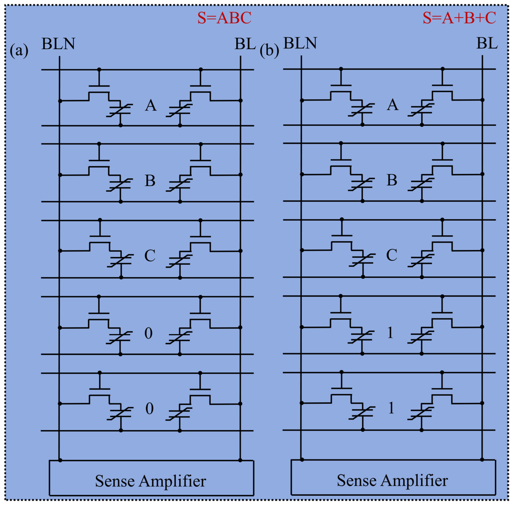
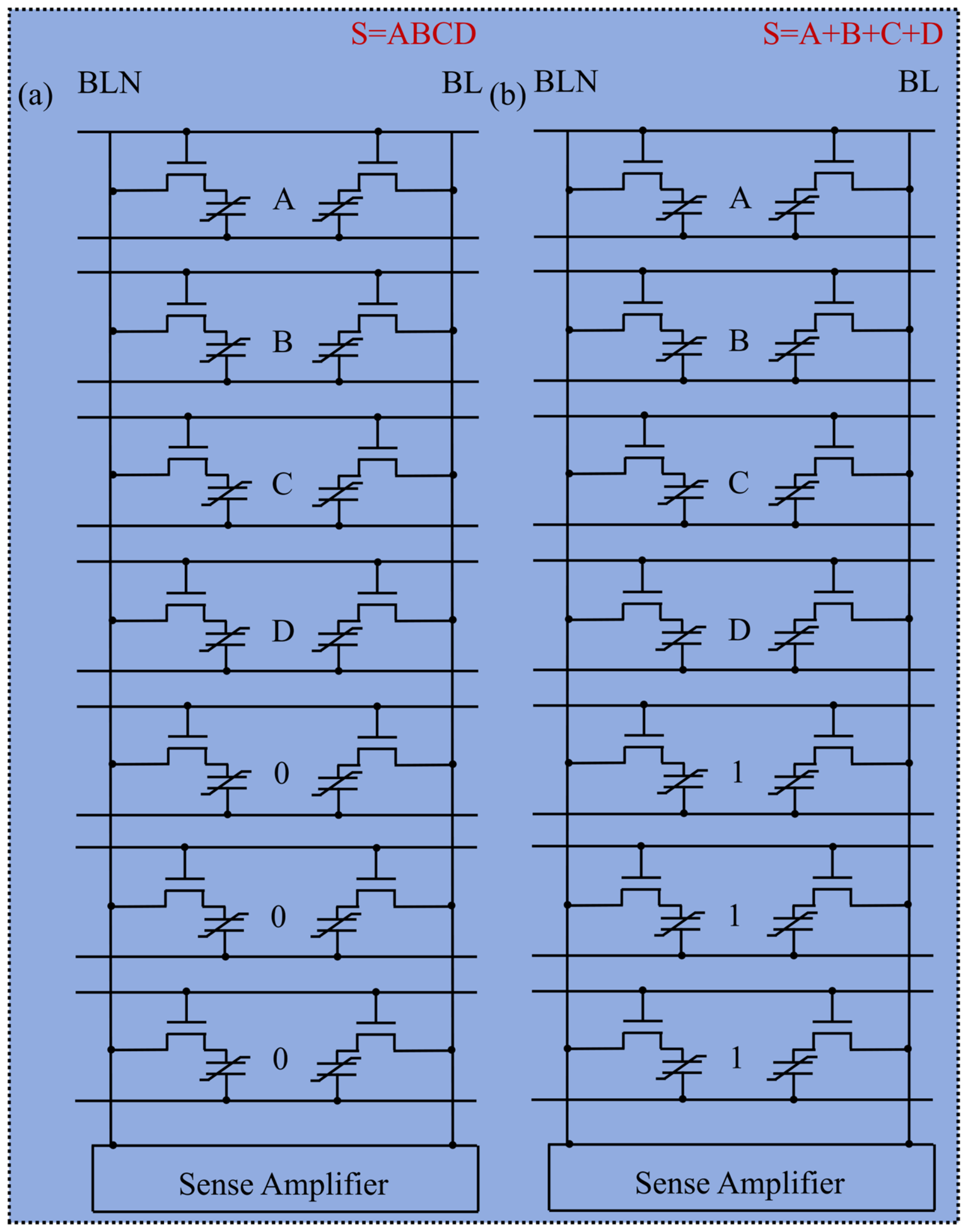
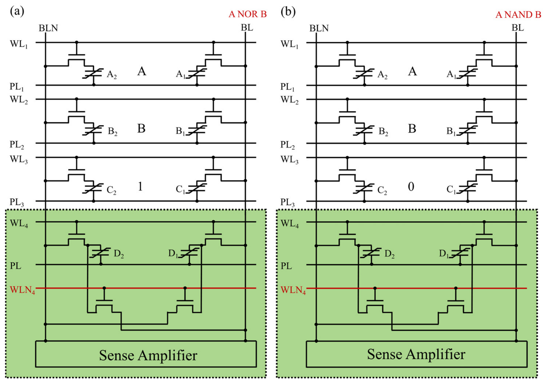
A 4T-2C FRAM cell with normal and cross-coupled bit-line access paths is introduced to support in-array inversion and complementary-result write-back. While the conventional 2T-2C cells perform majority-derived AND and OR operations through multi-row activation, the selectively embedded 4T-2C cells provide NOT functionality. Their combination enables NAND, NOR, functionally complete Boolean logic, and majority-based full-addition operations within the FRAM subarray.
HSPICE simulations indicate that the proposed FRAM CiM architecture provides a large sensing margin and stable sensing under the evaluated global PVT conditions: the minimum bit-line voltage difference reaches 337 mV during triple-row activation and 214 mV during quintuple-row activation, respectively. In addition, PVT simulations demonstrate less than 4.62% variation in the bit-line voltage difference over temperatures ranging from −40 °C to 125 °C.
The proposed architecture provides ADC-free bitwise computing with binary inputs and outputs, thereby avoiding the associated conversion-circuit overhead. The larger 4T-2C cells are selectively deployed only in dedicated computing rows, while conventional 2T-2C cells are used for dense data storage and majority computation. An 8 × 8 hybrid FRAM CiM prototype, consisting of six rows of 2T-2C cells and two rows of 4T-2C cells, was fabricated in a 180 nm CMOS process for physical implementation and basic array-level functional verification.
2. Background of 2T-2C FRAM Cell
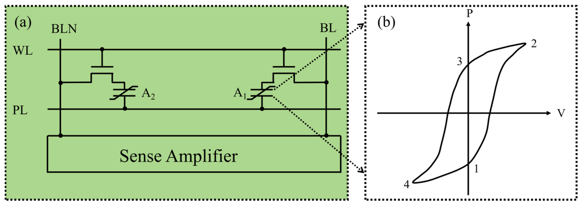
The structure diagram of the 2T-2C FRAM cell is shown in
Figure 1a. It consists of two transistors and two ferroelectric capacitors, one end of which is connected to the plate line (PL) and the other end is connected to a pair of complementary bit-lines (BL, BLN) through a transistor [
41]. The ferroelectric capacitor stores data according to its hysteresis loop, as shown in
Figure 1b [
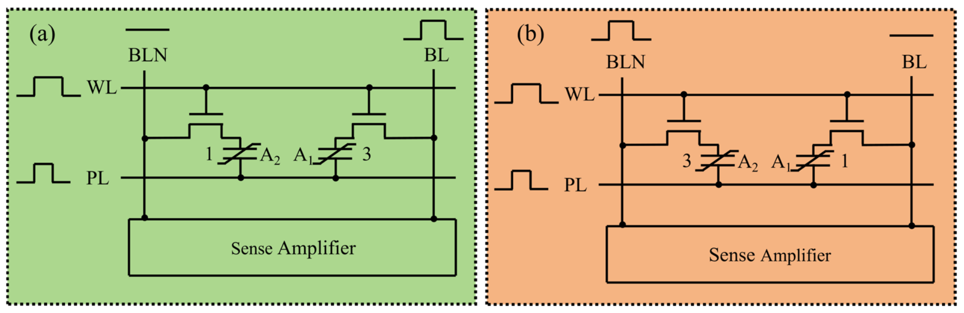
42]. When writing data “1” to the 2T-2C FRAM cell, a high voltage is applied at WL, ferroelectric capacitors A
1 and A
2 are connected to BL and BLN, and then a high voltage pulse is given at PL, while a high voltage pulse is given at BL and a voltage of 0 V is applied at BLN (
Figure 2a). At this time, the hysteresis loop of A
1 first reaches 2, and when the high voltage pulse on BL ends, the hysteresis loop of A
1 stays at 3. The hysteresis loop of A
2 reaches 4 first, and after the high voltage pulse on PL ends, the hysteresis loop of A
2 stays at 1. When reading data “1”, a high voltage is applied at WL, ferroelectric capacitors A
1 and A
2 are connected to BL and BLN, and then a high voltage pulse is given at PL, while both BL and BLN are subjected to 0 V. At this time, the hysteresis loop of A
1 starts at 3, and when the PL high voltage pulse is applied, the hysteresis loop of A
1 reaches 4, releasing charge Q
1 and forming voltage V
1 on BL. The hysteresis loop of A
2 starts at 1, and when the PL high voltage pulse is applied, the hysteresis loop of A
2 reaches 4, releasing charge Q
2 and forming voltage V
2 on BLN. Since Q
1 is larger than Q
2 and V
1 is larger than V
2, the sense amplifier will pull V
1 up to VDD and pull V
2 down to 0 V, finally resulting in a voltage of VDD on BL and 0 V on BLN, thus reading data “1”. When writing data “0”, the operation is the same as when writing data 1, except that a 0 V voltage is applied to BL and a high voltage pulse is applied to BLN (
Figure 2b). Reading the data “0” results in a voltage of 0 V on BL and VDD on BLN. The 2T-2C FRAM cell is fast-reading and non-volatile, making it suitable for in-memory computing.
4. The In-FRAM Full Adder Design
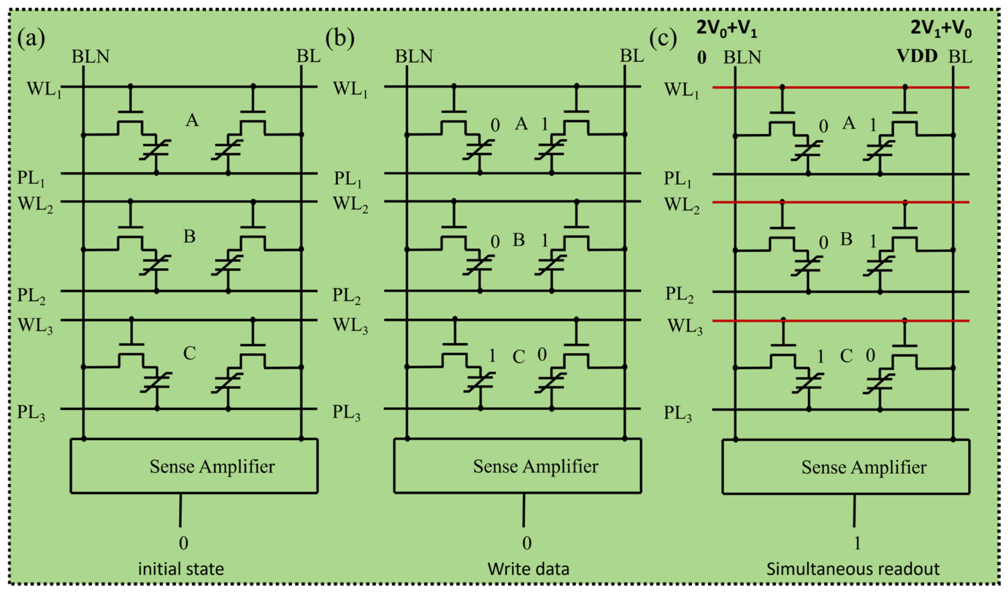
FRAM in-memory calculation involves reading the stored data by activating multiple WLs at the same time and obtaining the calculation results after amplification by the sense amplifier. Such calculations follow the majority function. In order to match the FRAM CiM subarray, we design the full adder based on the majority function. We calculate the carry-out and the sum using the following formula:
where A
i and B
i are the input data, C
i−1 is the input carry signal, C
i is the output carry signal, and S is the sum signal.
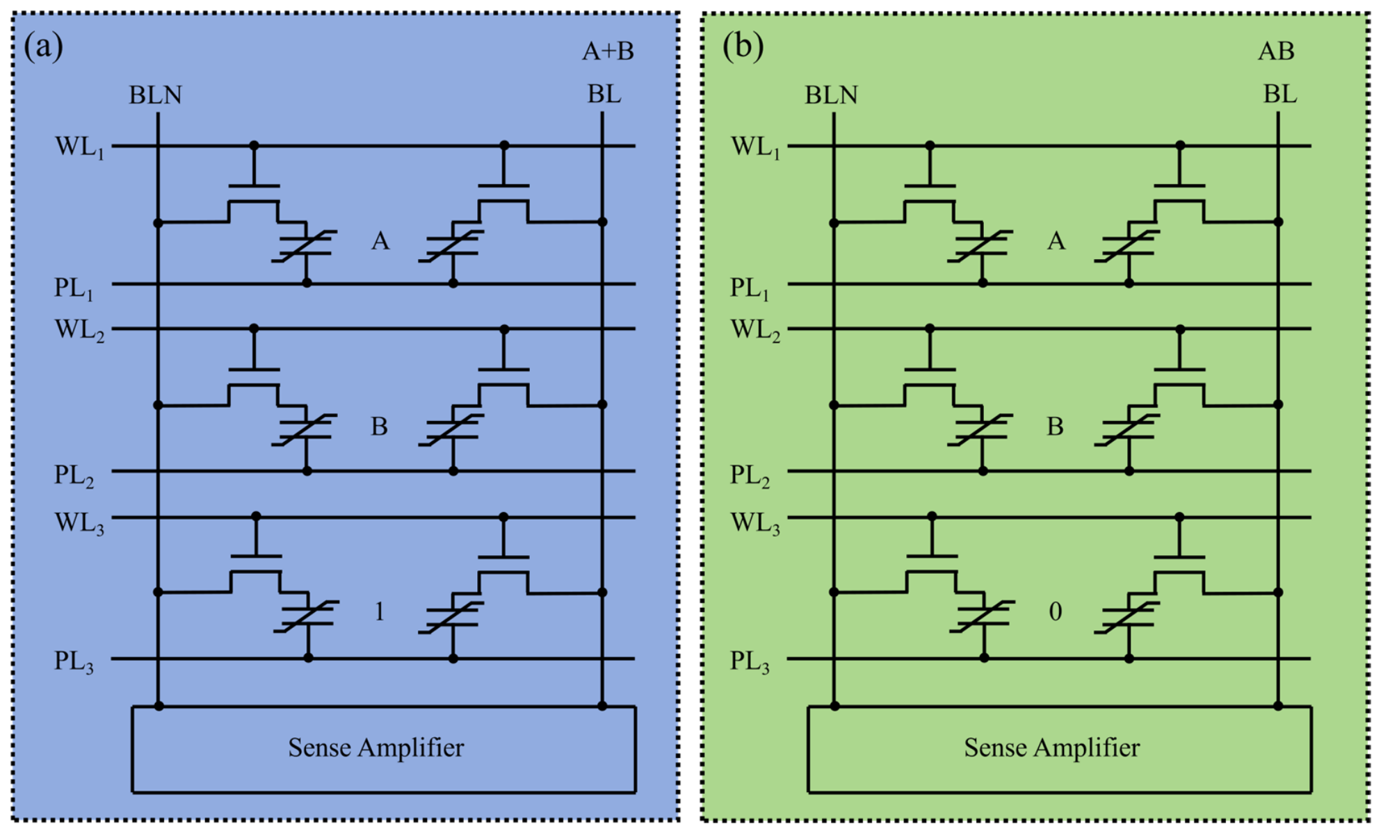
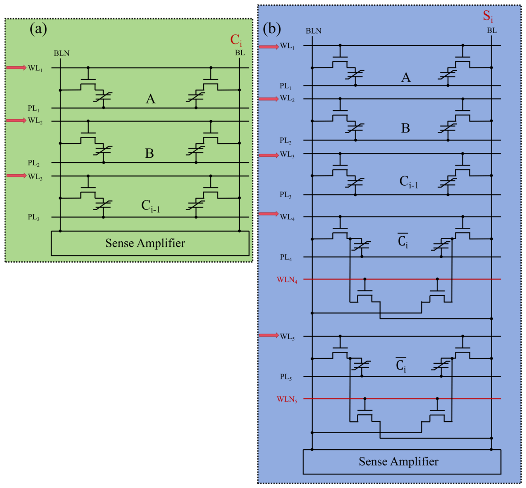
Under the FRAM CiM architecture, the full addition computation needs to be performed in two steps. The WLs corresponding to A, B and C
i−1 are first activated, and the carry output C
i is calculated according to the majority formula (
Figure 9a). It should be noted that the calculated C
i needs to be stored in two different 4T-2C cells to get the
data needed for the next calculation. Then, WLs corresponding to A, B, C
i−1 and two
are activated, and the calculated result sum is obtained on BL according to the majority formula (
Figure 9b).
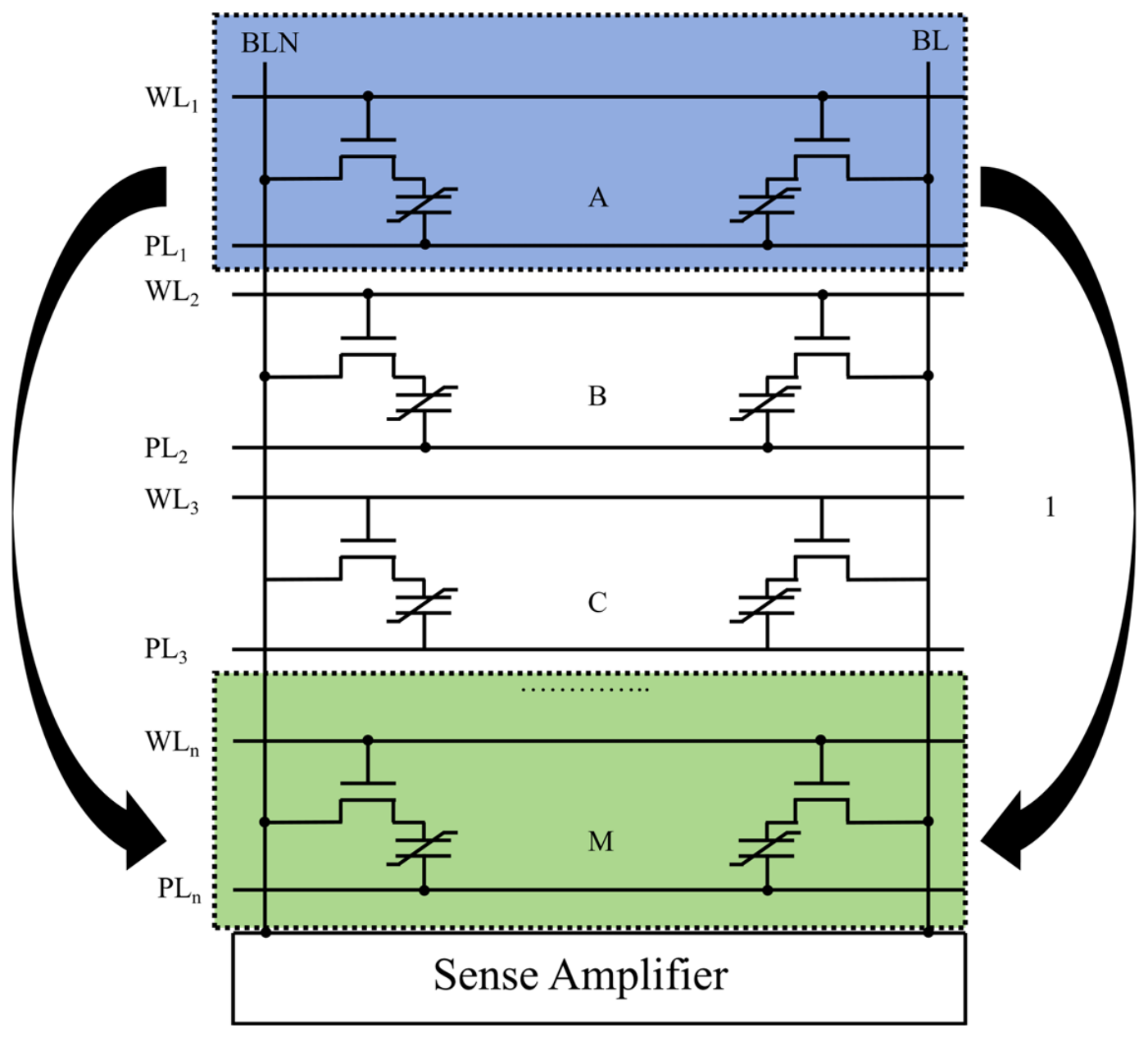
The data readout of the 2T-2C FRAM cell is destructive, so we adopt the method of copying data to avoid destructive readout of FRAM. Data in the same column of the FRAM subarray can be transferred from one row to another, as shown in
Figure 10. In a column of 2T-2C FRAM, data “1” is stored in cell A. First, a high voltage is applied to WL
1, and the data “1” in A is read out with the voltage pulse of PL
1. After resolution by the sense amplifier, the voltage on BL is VDD and the voltage on BLN is 0 V. A high voltage is applied to WL
n of the target M cell, and voltage pulses are applied to PL
1 and PL
n to write data “1” back to A and also to M. Finally, WL
1 and WL
n are turned off. Through the above operations, the data “1” is successfully copied from A to M without destroying the original data stored in A. Accordingly, one row-to-row replication comprises two sequential array-operation phases: (i) destructive readout and sensing of the source cell and (ii) simultaneous restoration of the source cell and writing of the destination cell. Each replication event, therefore, adds one read/sense phase and one restore/write phase before the subsequent CiM operation, and its energy overhead consists of the energy consumed by these two phases.
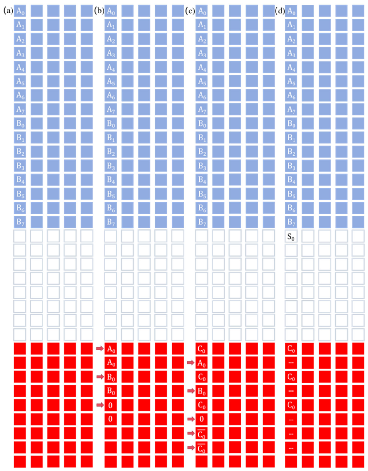
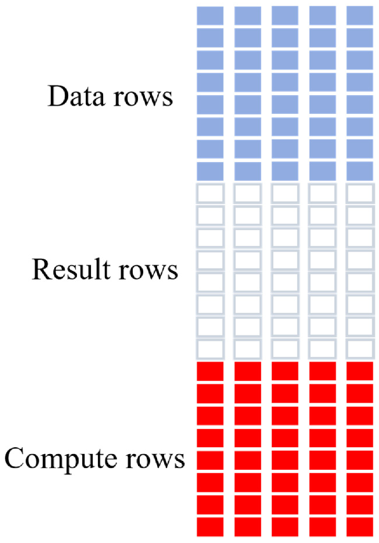
Therefore, the FRAM CiM subarray is divided into three parts: data rows, result rows and compute rows (
Figure 11). The data rows store the original input vectors, which are then copied to the compute rows for computation. This approach ensures that the original input data is not destroyed during the read-out process. The computed results are stored in the result rows, awaiting invocation or retrieval.
Based on the aforementioned FRAM CiM subarray, multi-bit full addition operations can be implemented. In the multi-bit full addition calculation, the lowest carry output (C
0) and sum (S
0) are calculated first. Then, C
1, S
1, C
2, S
2… are calculated. Taking the 8-bit full addition in the FRAM CiM architecture as an example (
Figure 12), first, the input vectors A and B are stored in the data rows (
Figure 12a). Then, A
0 and B
0 are copied from the data rows to the compute rows, and data “0” is written in the compute rows as the input carry (
Figure 12b). It should be noted that A
0 and B
0 are copied to two different FRAM cells, and the data “0” should be written to two different FRAM cells. This is because A
0, B
0 and “0” need to be read out twice in the subsequent calculation. A
0, B
0 and data “0” are then read out and calculated to get the output carry C
0. The C
0 is stored in the 2T-2C FRAM cell corresponding to the A
0, B
0, and data “0” that were read out previously.
is stored in two different 4T-2C cells (
Figure 12c). A
0, B
0, “0” and the two
are then read out to calculate the lowest sum signal (S
0). The calculated S
0 is written to the result rows. At this time, three 2T-2C FRAM cells in the compute rows are still storing C
0 data, which are used as the input carry to calculate the output carry of the higher bit (
Figure 12d). The serial calculation in FRAM memory ensures high accuracy in multi-bit calculation. Under this full addition computing architecture, the signal addresses in the compute rows are switched cyclically, making it convenient to design serial full addition computing. The input vector, output vector and all calculations are carried out in the FRAM computing-in-memory subarray, which reduces data transmission and cache, thereby reducing the transmission power consumption of the chip. Destructive readout during the bit-serial multi-bit full-adder operation in
Figure 12 is managed by performing majority reads on replicated operands in the compute rows, rather than on the original operands in the data rows. Within each BL/BLN column, bit positions are processed serially from the least to the most significant bit. Before bit
i, the replication operation in
Figure 10 copies A
i and B
i into designated compute rows while restoring the source cells; two working copies of A
i, B
i, and C
i−1 are prepared because these values are used in both the carry and sum evaluations. The first destructive majority read consumes one copy set and produces C
i, which is immediately written into the vacated 2T-2C working cells, while its complement is written into two 4T-2C cells. The second destructive majority read uses the remaining operand/carry copies and the two complementary carry values to produce S
i, which is written into the result row. The stored C
i then serves as the input carry for bit
i + 1, and the same compute rows are overwritten by the next operand copies and reused. Thus, destructive readout is confined to temporary compute-row copies, while the original multi-bit operands remain preserved in the data rows. Replication increases the number of polarization-switching events because each destructive read is followed by restoration. For context, HfZrO
x FRAM has demonstrated endurance of up to 10
12 cycles at 27 °C and 10
10 cycles at 120 °C [
43], providing a device-level reference for the additional access stress.
Within each column, successive full-adder bit positions are processed serially according to the schedule in
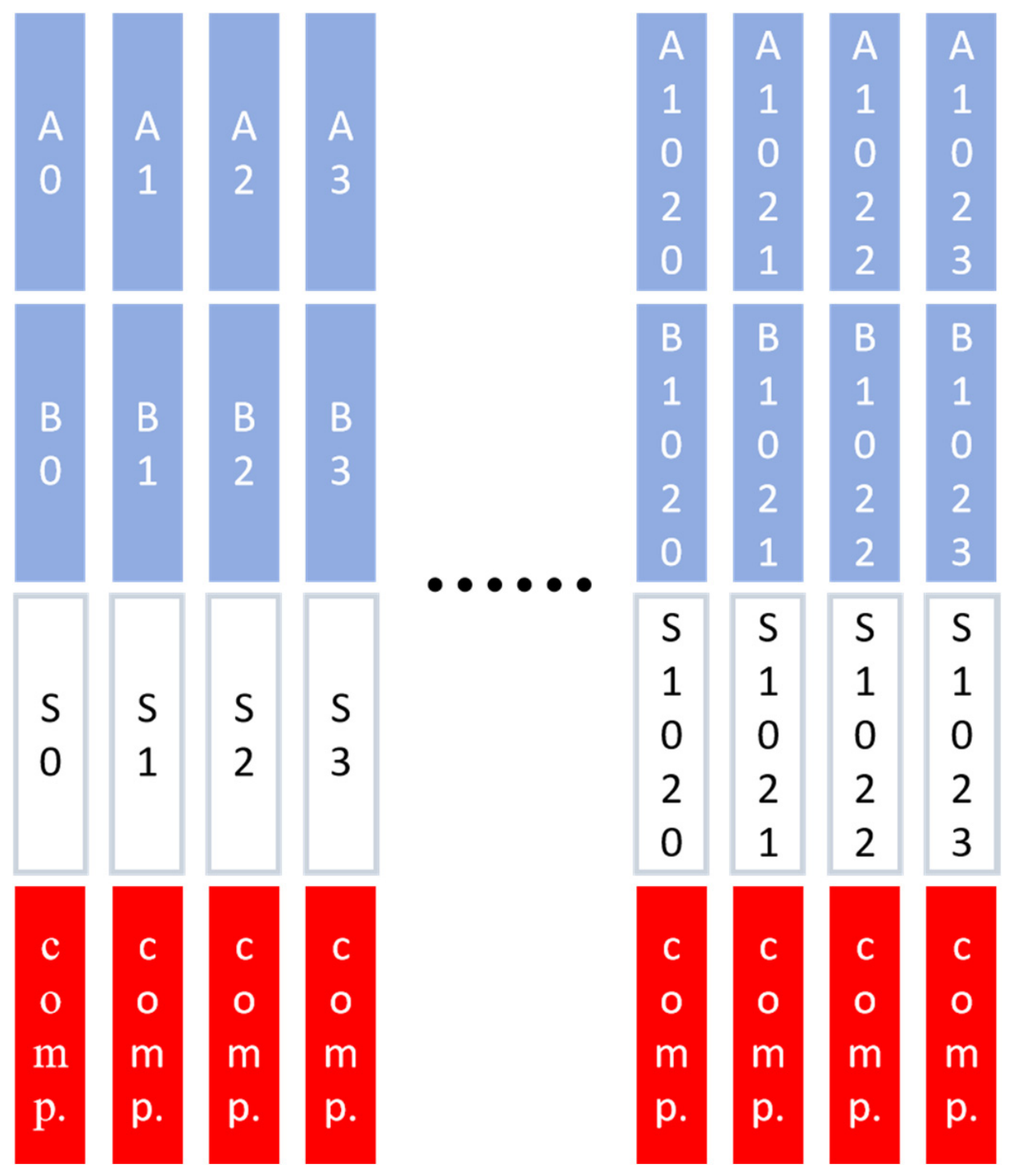
Figure 12, whereas independent columns can share the same WL/PL command sequence. Accordingly, the 512 × 1024 organization in
Figure 13 illustrates algorithmic column-level parallelism under uniform WL/PL delivery and adequate per-column sensing margin: 1024 independent 8-bit additions follow the same scheduled row-operation sequence as one 8-bit addition. This operation-count equivalence does not imply array-size-independent latency, energy, or sensing robustness because these quantities depend on array dimensions and interconnect loading, as discussed in
Section 5. In
Figure 13, A0–A1023 and B0–B1023 denote operand words, while sum0–sum1023 denotes the corresponding result words. The active column count and operand width depend on subarray partitioning and the target application.
5. Results and Discussion
To evaluate the functionality and PVT-dependent sensing stability of the proposed FRAM CiM circuit, HSPICE simulations were performed using a 180 nm CMOS process. All the ferroelectric capacitance models adopted the Lim model [
44,
45]. The circuit simulation power supply voltage, capacitance area and transistor parameters are shown in
Table 1.
Table 2 lists the principal parameters of the FeCAP Lim model.
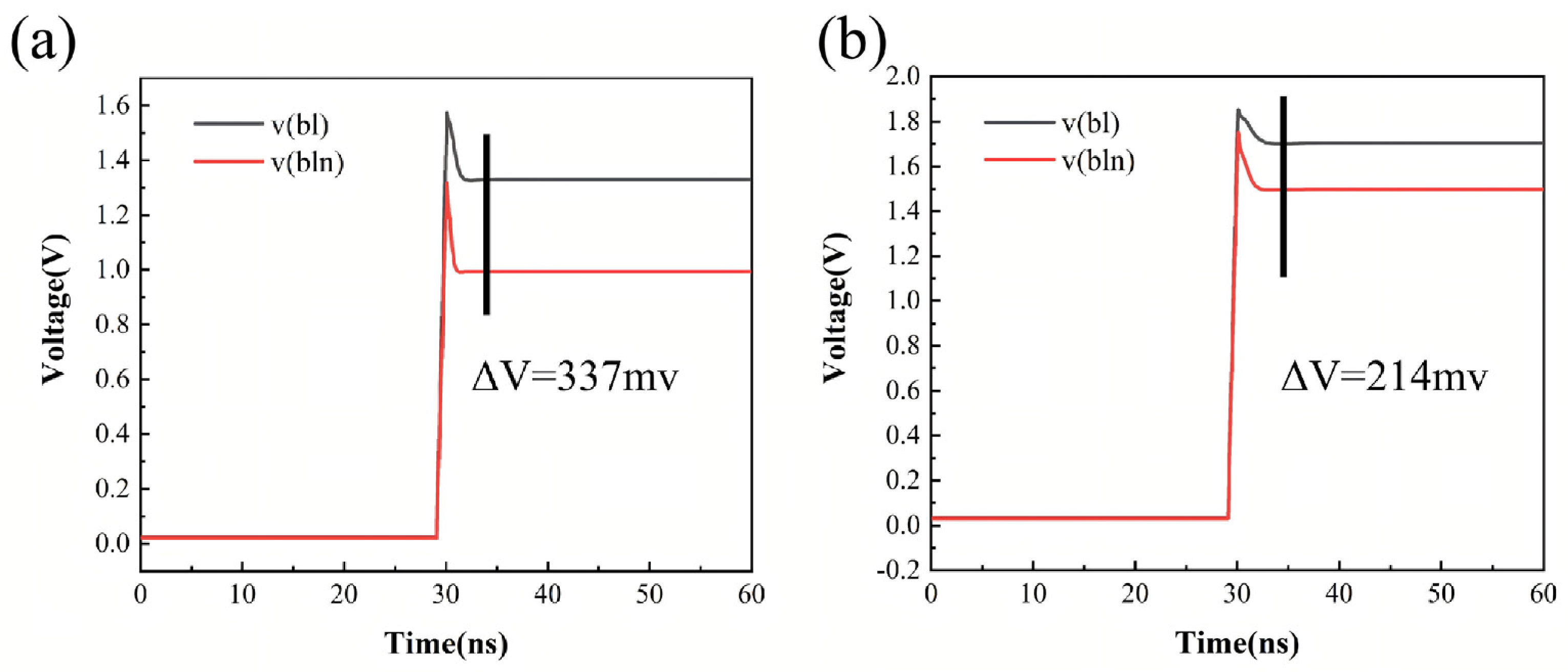
Figure 14a shows the transient simulation curve of the triple-row activation operation. In this operation, two of the three activated 2T-2C cells store data “1” and the others store data “0” (the voltage difference between BL and BLN is minimized). The three WLs are activated, and a high-voltage pulse is applied to the corresponding PL to read the cells.
Figure 14b shows the transient simulation curve of the quintuple-row activation operation. In this operation, three of the five activated 2T-2C cells store data “1” and the others store data “0” (the voltage difference between BL and BLN is minimized). The sense amplifier resolves the ΔV between BL and BLN and drives the complementary bit lines to VDD and 0 V, respectively. Therefore, the voltage difference between BL and BLN determines the accuracy and functionality of FRAM in-memory calculation. The ΔV of the triple-row activation operation proposed in this paper can reach 337 mV, which is much higher than the ΔV of the DRAM in-memory calculation circuit (only 65 mV,
Table 3) [
8]. These simulation results indicate a larger sensing margin than that of the referenced DRAM CiM circuit under the evaluated conditions.
In the practical application of the circuit, a load capacitance is typically present on each bit-line (bit-line capacitor) of the FRAM CiM subarray. The matching of bit-line capacitance in the FRAM CiM subarray is studied in this paper.
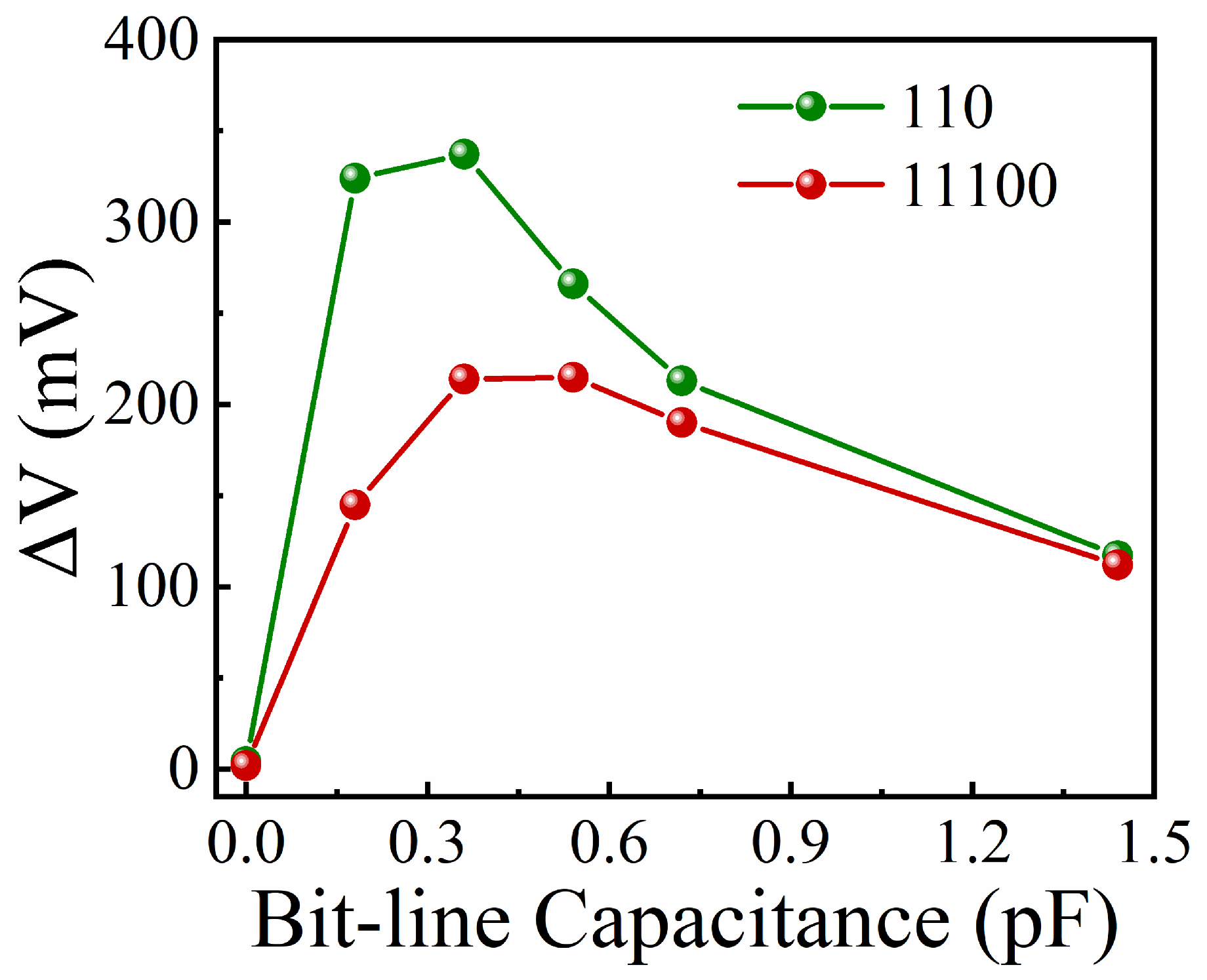
Figure 15 shows the ΔV resulting from a triple-row activation operation at 3.3 V with different bit-line capacitors when the stored data is “110”. When the bit-line capacitance is increased to 0.36 pF, the bit-line ΔV reaches a maximum of 337 mV. Continuing to increase the value of the bit-line capacitance causes the ΔV to decrease, and when the bit-line capacitance reaches 1.44 pF, the ΔV decreases to 117 mV.
Figure 15 also shows the ΔV resulting from a quintuple-row activation operation at 3.3 V with different bit-line capacitors when the stored data is “11100”. When the bit-line capacitance is increased to 0.54 pF, the bit-line ΔV reaches a maximum of 215 mV. However, when the bit-line capacitance is 0.36 pF, ΔV can also reach 214 mV, which is very close to the maximum value of ΔV. Similar to the triple-row activation operation, increasing the value of the bit-line capacitance causes the ΔV to decrease, and when the bit-line capacitance reaches 1.44 pF, the ΔV decreases to 112 mV. Considering both scenarios of triple-row and quintuple-row activation operations in computational requirements, a bit-line capacitance of 0.36 pF exhibits optimal compatibility with the FRAM CiM subarray.
Array scaling introduces different parasitic loads along the two array dimensions. Increasing the number of cells sharing a BL/BLN and the associated wire length increases bit-line capacitance and distributed resistance. Under the charge-sharing relation in Equation (1), the polarization-dependent charge is resolved against this load; once Cb exceeds its operating optimum, additional capacitance reduces ΔV and increases settling time.
Figure 15 directly shows this sensitivity: increasing Cb from 0.36 to 1.44 pF reduces ΔV from 337 to 117 mV for triple-row activation and from 214 to 112 mV for quintuple-row activation. These results indicate that bit-line segmentation, the sensing point, and the array dimensions must be co-optimized. Measurements of 2T-2C FeRAM circuits have likewise related bit-line capacitance to the number of connected cells and metal parasitics, while identifying the highly capacitive plate line as a major component of access timing [
46].
Increasing the number of columns increases the WL fanout to access-transistor gates and the PL load presented by ferroelectric-capacitor electrodes. Their distributed RC delay produces position-dependent rise/fall times and pulse skew, so far-end cells may be activated later or experience a different effective PL pulse. Multi-row activation imposes a separate, data-dependent constraint. For an odd-N majority operation at the nearest decision boundary, the useful polarization-charge excess corresponds to one cell while the total connected capacitance grows with N; under the idealized assumptions of Equation (1), the initial differential therefore tends to decrease. This is not a universal monotonic relation with row count because operand replication or a larger majority imbalance can increase the net charge difference. The allowable activation count must satisfy the worst-case ΔV relative to sense-amplifier offset and noise, together with decoder, WL/PL-driver, timing skew, peak current, and restoration constraints; related charge-sharing CiM analyses explicitly include BL/WL resistance, capacitance, and component variation [
30]. Septuple-row and higher-order operations should consequently be evaluated against the same worst-case margin criterion. Practical scale-up would therefore use segmented subarrays and short local bit lines [
40], local sense amplifiers, hierarchical or repeated WL/PL drivers, and bounded multi-row activation groups.
To evaluate the sensing stability of the FRAM CiM circuit under global PVT conditions, PVT simulations were conducted by varying three critical parameters: process corners, polarization voltage, and temperature. The simulation results are summarized in
Table 4 and
Table 5. Specifically,
Table 4 presents the PVT simulation during triple-row operations when the stored data pattern was “110”. Notably, variations in FRAM polarization voltage directly influence the polarization strength of ferroelectric capacitors, which governs bit-line voltage fluctuations. Consequently, an increase in polarization voltage leads to enhanced ΔV on the bit-line. When varying process corners and temperature in the FRAM CiM circuit, the bit-line ΔV exhibited only minor fluctuations of a few mV. Similarly, during quintuple-row activation operations with the stored data pattern “11100”, ΔV variations remained negligible under altered process corners and temperature conditions (
Table 5). PVT analysis showed <4.62% ΔV variation across the evaluated temperature range (−40 °C to 125 °C) for the triple-row and quintuple-row activation operations at 3.3 V. In FRAM CiM arrays, the output signal is achieved by amplifying the bit-line ΔV through a sense amplifier. Consequently, the stability of ΔV is a direct indicator of sensing stability under the evaluated global PVT conditions. The PVT simulation results indicate stable bit-line voltage differences across the evaluated process corners, polarization voltages, and temperatures.
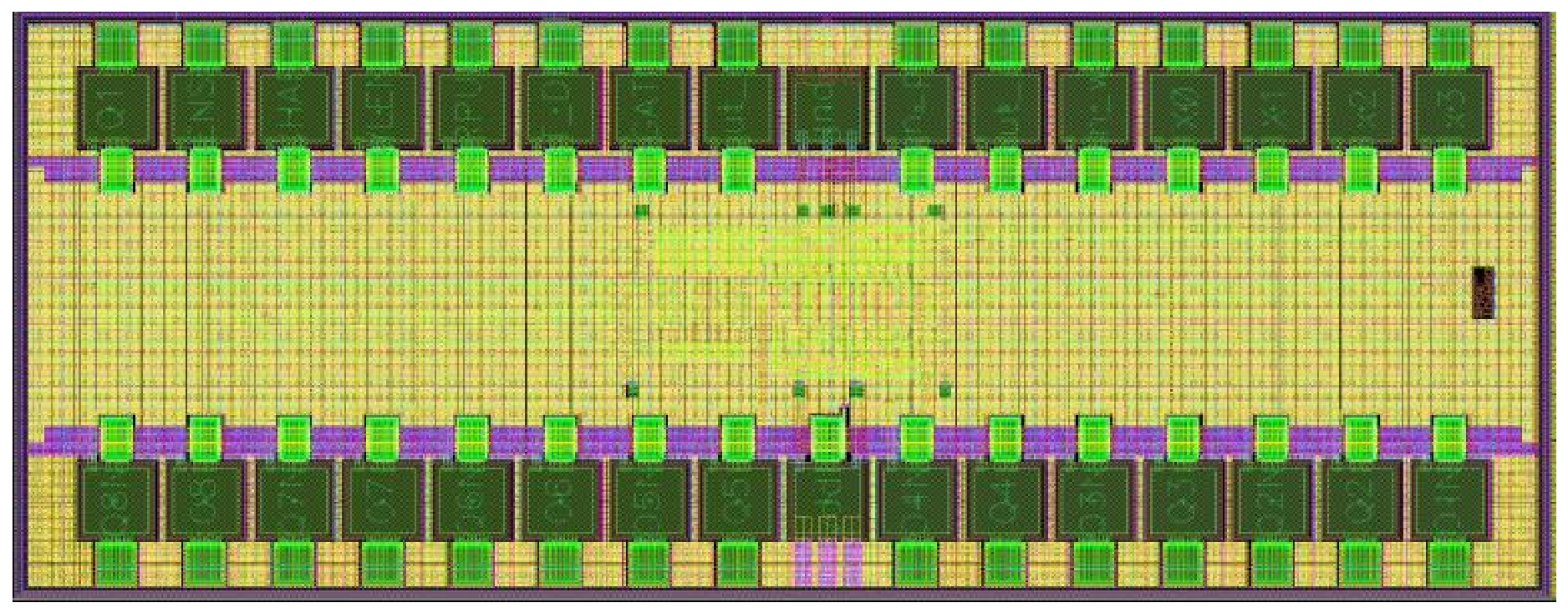
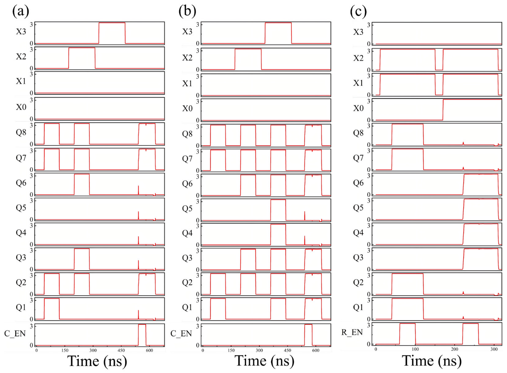
Figure 16 shows the layout of the 8 × 8 FRAM CiM circuit, which comprises six rows of 2T-2C FRAM cells, two rows of 4T-2C cells, and peripheral circuits. The size of the FRAM CiM circuit is 1930 um × 1080 um. SPICE simulations were conducted for the 8 × 8 FRAM CiM circuit, as shown in
Figure 17. In this configuration, X
3, X
2, X
1, and X
0 represent the 4-bit address signals, Q
1–Q
8 denote the data channels, and C_EN serves as the computation enable signal. When C_EN is at a logic-low level, the simulated circuit operates in the standard read/write mode, allowing data to be written into or read from the FRAM cells. When C_EN is asserted high, the circuit enters the computing mode and performs bitwise operations on the stored 8-bit data.
To further evaluate the performance of the proposed FRAM CiM architecture, the energy consumption and calculation latency of the OR, AND, and NOT operations were extracted from transient HSPICE simulations of the 8 × 8 FRAM CiM compute-array circuit model. The simulated circuit model includes the hybrid 2T-2C/4T-2C FRAM compute array, the address decoder, word-line boosting/driver circuitry, plate-line transmission circuitry, discharge modules, bit-line data paths, and sense amplifiers. The energy consumption per bit was obtained directly from the transient HSPICE simulation of one 8-bit parallel computing operation and normalized by the eight output bits. The simulated calculation latency was extracted from the activation of the computing control signals to the stabilization of the sensed output. As summarized in
Table 6, the OR and AND operations exhibit nearly identical energy consumption and latency because their operation sequences are the same, with the only difference being the logic value stored in the preset 2T-2C cell. The NOT operation is performed using the cross-coupled access paths of the 4T-2C cell and requires a different operation sequence.
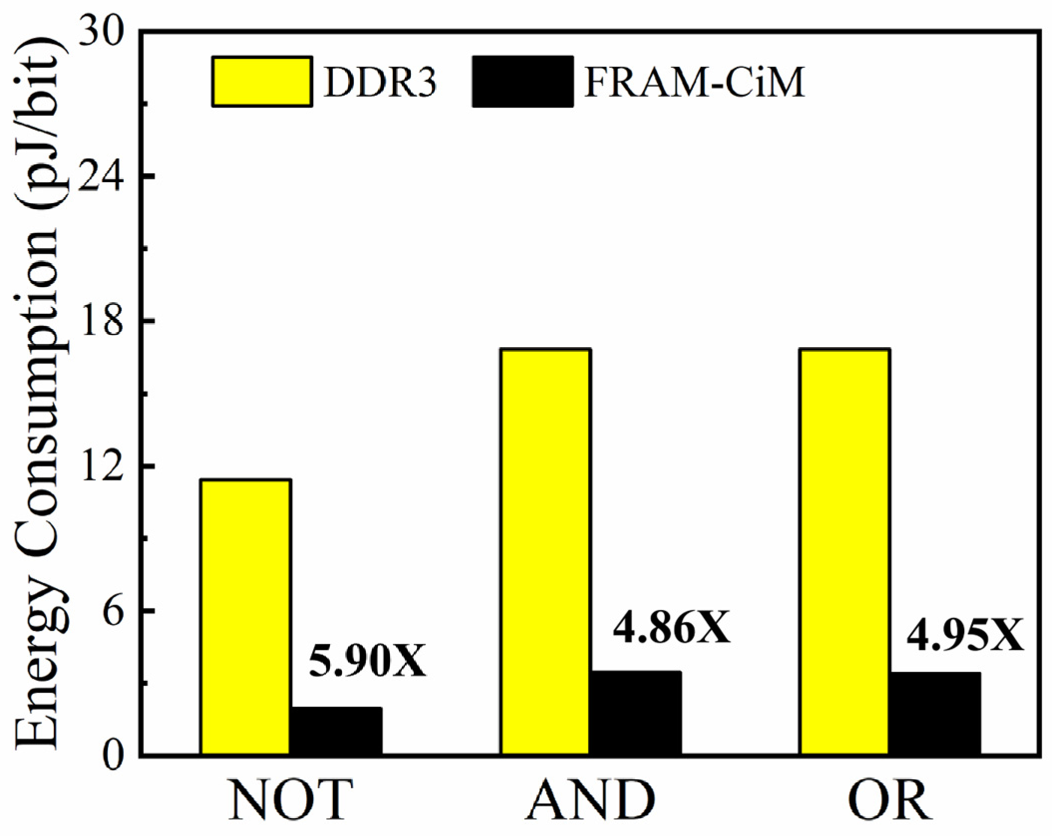
Figure 18 compares the simulated FRAM energy with the DDR3-interface baseline in [
30]. The DDR3 result includes DRAM and DDR3-channel energy, whereas the FRAM result includes the compute array and its peripheral circuits. Both results include their respective memory-side circuitry and exclude processor energy. Across the evaluated bitwise operations, the proposed FRAM CiM architecture reduces energy consumption by 4.86×–5.90× compared with the DDR3-based design.
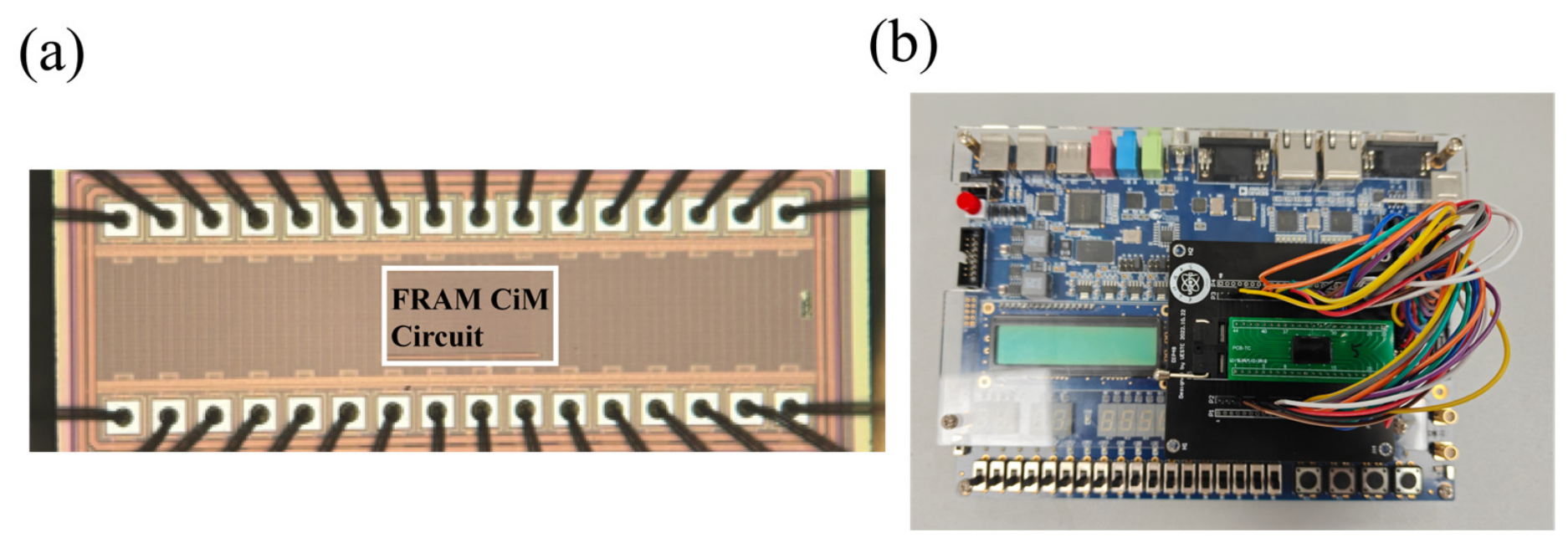
As a physical implementation of the proposed hybrid architecture, an 8 × 8 FRAM CiM prototype was fabricated in a 180 nm CMOS process. As shown in
Figure 19a, the fabricated prototype integrates six rows of conventional 2T-2C FRAM cells, two rows of 4T-2C FRAM cells, and the associated peripheral circuits.
Figure 19b shows the FPGA-based test setup, which consists of a DE2-115 FPGA board, the fabricated FRAM CiM prototype, and a dedicated test PCB. The FPGA-based setup was used to verify the basic functionality of the fabricated array, while the quantitative CiM performance results reported in this work were obtained from HSPICE simulations.
To provide a broader cross-technology context,
Table 7 compares the proposed FRAM CiM circuit with representative Boolean CiM designs based on SRAM [
47], DRAM [
48], RRAM [
49], and MRAM [
50]. Energy consumption is expressed in pJ/bit, and calculation latency in ns.
As shown in
Table 7, the proposed FRAM CiM circuit achieves calculation latencies of 0.599 ns for OR and AND and 1.167 ns for NOT. Within the reported results, these values demonstrate low computation latency despite the use of mature 180 nm technology. The short latency is mainly enabled by the 8-bit parallel operation and the direct sense-amplifier-based binary sensing path, which avoids ADC/DAC conversion. Moreover, the hybrid 2T-2C/4T-2C array provides a functionally complete OR, AND, and NOT set while retaining nonvolatile storage.
The simulated energy consumption of 1.94–3.46 pJ/bit is higher than the reported values of several comparison designs. This difference is partly attributable to the mature 180 nm technology and to the present simulation boundary, which includes the 8 × 8 compute array, word-line boosting and driver circuitry, plate-line transmission circuitry, discharge modules, bit-line data paths, and sense amplifiers.
Beyond the bitwise Boolean CiM designs summarized in
Table 7, the RRAM work in [
51] presents application-specific analog and hybrid-domain architectures for polynomial transformation, neural-network inference, and intelligent decision-making, whereas the PCM core in [
52] implements large-scale signed analog MVM with multibit input/output conversion and drift/temperature compensation. In contrast, the proposed FRAM architecture targets functionally complete bitwise Boolean computation: conventional 2T-2C cells provide majority-derived AND/OR, selectively embedded 4T-2C cells provide in-array inversion and complementary-result write-back, and the charge-sharing/sense-amplifier path produces binary outputs without ADC/DAC conversion. Accordingly, the novelty of this work lies in the hybrid-cell FRAM organization that combines nonvolatile storage, Boolean completeness, and full-adder support within the same subarray.