1. Introduction
Ultra-high voltage direct current (UHVDC) transmission has become a key technology for large-scale energy resource allocation and the realization of “dual-carbon” goals, owing to its advantages of high capacity, low losses, and flexible controllability [
1,
2,
3,
4,
5]. Conventional line-commutated converter (LCC) valves based on thyristors exhibit high efficiency and good economic performance. However, their inherent susceptibility to commutation failure poses a serious threat to the stability of weak receiving-end AC systems [
6,
7,
8,
9]. With the increasing penetration of renewable energy, system inertia continues to decrease, which further aggravates the risk of cascading commutation failures and restricts the development of UHVDC technology [
10,
11].
To mitigate commutation failure, extensive efforts have been made in both academia and industry, including the installation of synchronous condensers [
12], static var compensators [
13,
14], and the adoption of voltage source converter (VSC-HVDC) technology [
15,
16]. However, the use of auxiliary equipment increases system complexity and maintenance costs. Meanwhile, VSC-HVDC still suffers from relatively high losses under ultra-high power transmission conditions.
In recent years, the Controllable Line-Commutated Converter (CLCC) has been proposed as a promising solution [
17,
18,
19]. By introducing fully controlled devices into the valve arm, CLCC enables active turn-off capability [
20,
21], thereby ensuring reliable thyristor recovery even under severe AC voltage sags. The successful commissioning of the ±500 kV Ge-Nan HVDC renovation project in China in 2023 marked the practical application of CLCC technology in engineering [
22]. Existing studies on CLCC mainly focus on the “direct-string” topology, in which fully controlled modules are connected in series with thyristors. However, in this structure, the fully controlled devices are required to withstand the full DC current during normal operation and commutation processes. Although IGBT devices with ratings of 4.5 kV/2000 A or 4.5 kV/3000 A have been applied in HVDC engineering [
23,
24], higher-current devices suitable for large-capacity UHVDC applications (e.g., 6.5 kV/5 kA) remain technologically immature. Therefore, conventional direct-string CLCC topologies face considerable challenges in meeting the requirements of high-current UHVDC systems, where the current-carrying capability and thermal stress of fully controlled devices become critical constraints.
To overcome the limitations of conventional direct-string CLCC in high-current UHVDC applications, this paper proposes a high-reliability cascaded H-CLCC valve topology. Distinct from traditional direct-string structures, the proposed H-CLCC utilizes a cascaded H-bridge configuration that establishes a dual-path conduction mechanism in steady state. By distributing the DC current across multiple parallel paths, this configuration effectively bypasses the current rating bottlenecks of conventional CLCC designs. This feature effectively reduces the current stress on individual IGBTs and diodes, which is beneficial for modular design and device selection in high-current DC applications. Furthermore, to enhance system reliability under fault conditions of fully controlled sub-valves (e.g., device failure or communication loss), a redundant configuration is designed, where a two-stage cascaded H-bridge is connected in parallel with bypass thyristors. This structure enables faulty modules to quickly exit CLCC operation and revert to LCC mode, thereby ensuring high system availability. In addition, a detailed analytical model based on the Laplace transform is established to characterize the dynamic behavior of capacitor voltage, providing a theoretical basis for capacitance design. Simulation results obtained from the PSCAD/EMTDC platform demonstrate that the proposed H-CLCC exhibits strong fault ride-through capability and self-recovery performance under extreme conditions.
2. Topology Configuration and Design
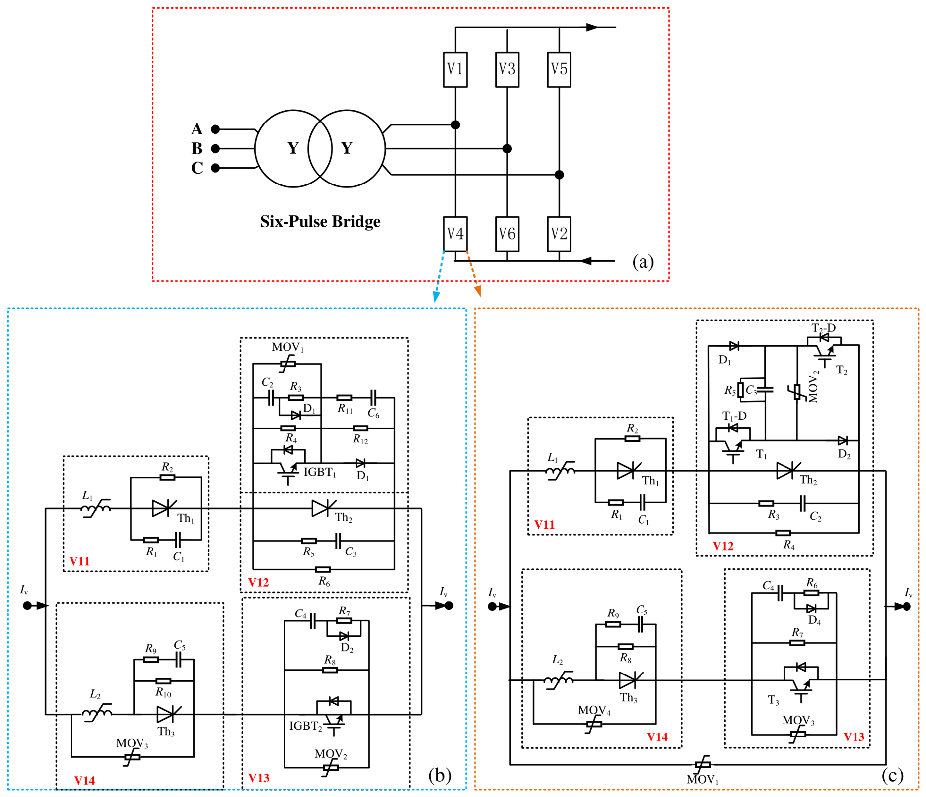
The topologies of the six-pulse commutation bridge, traditional CLCC, and H-CLCC converter valves are shown in
Figure 1a, b, and c, respectively. The H-CLCC topology is substantially consistent with the traditional CLCC, primarily consisting of two functional sections: the main branch and the auxiliary branch. The main branch is formed by the series connection of sub-valves V11 and V12, while the auxiliary branch comprises sub-valves V13 and V14 in series. The main branch serves as the primary conduction path during steady-state operation, optimizing efficiency and power density. Sub-valve V11 is identical to that of thyristor valves for HVDC, consisting of a thyristor level in series with a saturable reactor (
L1). As the primary conduction component, the thyristor (Th1) is utilized for its high power capacity, low conduction loss, high voltage rating, and superior cost-effectiveness [
20]. The thyristor level also integrates auxiliary components, including snubber resistors (
R1), snubber capacitors (
C1), DC grading resistors (
R2), and thyristor control equipment. The auxiliary branch is designed to divert and interrupt high-magnitude fault currents. Sub-valve V13 is constructed using multi-level, series-connected IGBTs. To ensure dynamic voltage balancing across the series string, each IGBT (T
3) is shunted with an RCD snubber circuit (
R6,
R7,
C4, and
D4). The structure of V14 is identical to that of V11, consisting of a thyristor level (Th
3), snubber circuit (
R9,
C5), DC grading resistors (
R8) and a saturable reactor (
L2). It provides the necessary voltage blocking and current-carrying capabilities during the fault interruption sequence.
The primary difference between the H-CLCC and the traditional CLCC valve lies in the topology of sub-valve V12. Unlike the direct-string IGBT structure employed in traditional CLCC valves, the H-CLCC sub-valve V12 adopts an H-bridge configuration, which is composed of an H-bridge assembly and an energy-dissipation branch (MOV
2). The former is composed of diodes (D
1, D
2), IGBTs (T
1, T
2) with their respective anti-parallel diodes (T
1-D, T
2-D), and capacitors (C
3), serving to facilitate current conduction and commutation control. During the conduction process, each IGBT device carries only half of the rated DC current, significantly reducing the current stress on individual components. Detailed conduction mechanisms are elaborated in
Section 3. Furthermore, V12 incorporates a bypass thyristor along with its associated damping and grading circuits (
R3,
C2 and
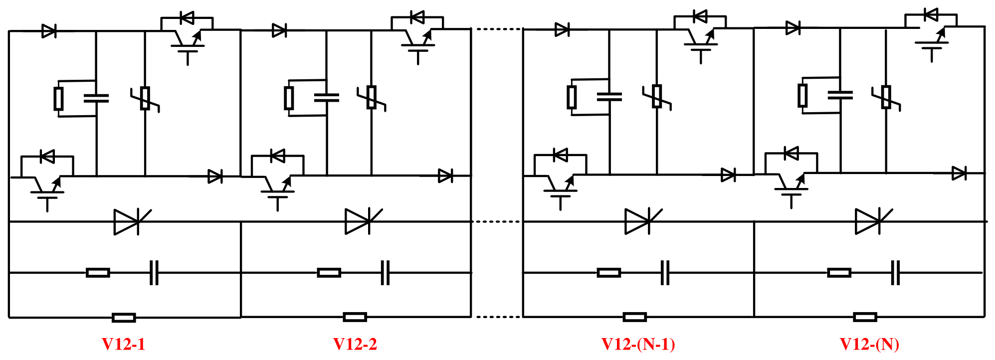
R4). It is worth noting that to enable V12 to exit CLCC mode and revert to LCC mode following an H-bridge failure, a topology consisting of two-stage H-bridges in series, paralleled with two-stage thyristors, is adopted, as shown in
Figure 2. Consequently, the number of levels
N for the H-CLCC sub-valve V12 must be an even integer. When a failure occurs in one H-bridge level, the faulty level and its adjacent level (both of which are configured under the same set of bypass thyristors) will simultaneously exit the CLCC mode. The rationale behind this design is that in a single-stage configuration (one thyristor paralleled with one H-bridge), an H-bridge failure—such as a T
1/T
2/C
3 breakdown—would prevent the establishment of the necessary forward voltage drop required to trigger the bypass thyristor, thereby failing to secure a reliable bypass path.
To further demonstrate the advantages of the proposed H-CLCC topology, a quantitative comparison among conventional LCC, direct-string CLCC, and H-CLCC is presented in
Table 1. The comparison focuses on topology configuration, applicable current level, commutation capability, and power loss.
Compared with conventional LCC, both CLCC and H-CLCC provide active turn-off capability, enabling improved immunity against commutation failure. However, the direct-string CLCC topology requires the fully controlled devices to carry the full DC current, which limits its application in high-current HVDC systems due to semiconductor current capability constraints. The proposed H-CLCC introduces cascaded H-bridge cells in the controllable sub-valve. Through the dual-path conduction mechanism, the DC current can be shared among multiple semiconductor devices, reducing the current stress of individual IGBTs and diodes. The semiconductor components are selected to accommodate a continuous 1.2 p.u. overload current requirement. Benefiting from the steady-state dual-path conduction of the H-bridge, each IGBT carries only 0.5 p.u. of the rated current (Id/2). This stress shunting enables 5 kA-class UHVDC applications using commercially mature 4.5 kV/3 kA IGBTs. Although the increased number of semiconductor devices results in slightly higher losses (approximately 0.346%), the proposed topology provides improved scalability for 5 kA-class HVDC applications while retaining the active commutation capability of CLCC.
It is worth noting that the use of bypass thyristors to clear faults and maintain normal system operation after an H-bridge device failure is subject to certain constraints. To ensure that the transfer branch can be reliably triggered under both steady-state and transient fault conditions, the DC voltage established by the H-bridge when interrupting the main branch current must exceed the break-over diode (BOD) triggering voltage of the two-stage V14 thyristor valve. Considering the voltage imbalance factor (
ki) and extreme operating conditions (N-stage BOD of the V14 sub-valve), the minimum number of series-connected H-bridge stages is defined as:
where
Vmov is determined by the initial threshold voltage of the energy-dissipation branch in each H-bridge stage. Consequently, if the number of H-bridge stages operating in CLCC mode falls below
, the entire arm will exit CLCC mode and revert to LCC operation. Under these conditions, the system remains operational but lacks the capability to mitigate commutation failure.
From an operational control perspective, there is no technical upper limit on N. However, in practical engineering applications, increasing N linearly elevates initial equipment capital costs and steady-state power dissipation. Thus, N is chosen to satisfy the system nominal voltage requirement and N + x redundancy while avoiding unnecessary cost and loss penalties.
3. Control Sequence and Operational Principles of H-Bridge
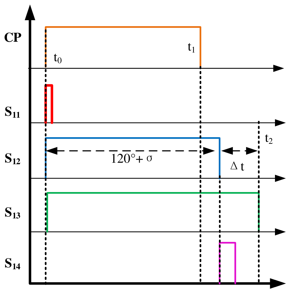
During normal operation, the switching sequence of the CLCC converter valve is illustrated in
Figure 3. At
t0, valve V11 is triggered, and the valve controller simultaneously sends firing pulses to sub-valves V12 and V13, establishing the conduction of the main branch. At
t1 (
t0 + 120° + σ), the IGBTs in the main branch sub-valve V12 are turned off, while the thyristors in the auxiliary branch sub-valve V14 are triggered. Consequently, the current begins to commutate from the main branch to the auxiliary branch. Given that σ > 0°, the moment t
1 occurs after the turn-on of arm VT3. Finally, at
t2 (
t1 + Δ
t), the IGBTs in the auxiliary branch sub-valve V13 are turned off, achieving zero-current switching. It is worth noting that under fault conditions, the turn-off of V12 and the triggering of V14 must be advanced to
t1 (a moment prior to the normal schedule) to facilitate the rapid transfer and subsequent interruption of the fault current.
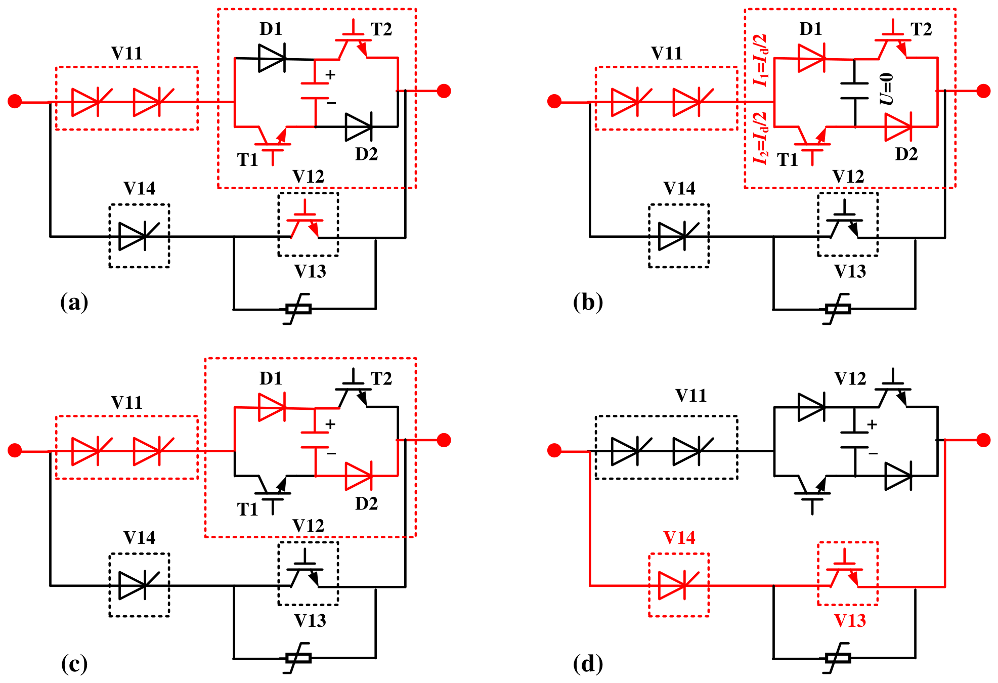
The current transition process of the H-CLCC during operation is illustrated in
Figure 4. Upon receiving the trigger pulse from the pole control system (t0), the valve control unit issues a signal to turn on V11, V12, and V13. Since V14 remains in a blocked state, the entire current initially flows through the main branch. Driven by the pre-charged voltage of the H-bridge capacitor C
3, the current first follows the T
1-C
3-T
2 path, as illustrated in
Figure 4a. Once the capacitor voltage discharges to zero, diodes D
1 and D
2 become forward-biased, leading to a dual-path conduction state within the H-bridge where each branch carries half of the rated current, as shown in
Figure 4b. Consequently, the H-CLCC can achieve high-capacity current conduction by utilizing power electronic devices with relatively lower current-carrying capacities. Specifically, IGBT components with a rated current of 0.5 p.u. are sufficient to meet operational requirements. Furthermore, during AC faults, the DC current level at the inverter side does not exceed twice the rated current, whereas the maximum turn-off capability of modern IGBTs can reach more than five times their own rated current [
20,
24]. Therefore, selecting the V12 IGBTs based on 0.5 times the rated DC current level is also sufficient to satisfy the turn-off requirements. At the falling edge of the pole control signal (after t1), the valve control unit issues a turn-off command to V12, shifting the current from the dual-path conduction mode to the C3 charging mode in
Figure 4c. Simultaneously with the V12 turn-off, V14 is triggered. As the accumulation of charge on C3 raises the voltage to the minimum turn-on threshold of V14, the current begins to transfer from the main branch to the auxiliary branch, as depicted in
Figure 4d. Detailed current characteristics are provided in
Section 5.
During normal operation, sub-valve V12 turns off when the main branch current decreases to a preset threshold between 0.7 kA and 1.3 kA, which allows the H-bridge capacitor C3 to build up a voltage margin of 1 kV to 2 kV for gate-drive energy harvesting. Under fault conditions, V12 turn-off and V14 triggering are initiated by the falling edge of the pole control signal. Considering controller processing latency and thyristor turn-on delays, the total execution delay is bounded within 25 µs. The selected H-bridge capacitance provides adequate design margin during this 25 µs window, enabling C3 to rapidly establish the required forward voltage and ensure successful forced commutation under severe 8 kA fault currents. Furthermore, integrating transient di/dt detection into local valve control to dynamically optimize turn-off timing and minimize power losses—such as implementing timer-based turn-off strategies for decaying fault currents or adaptive turn-off timings for varied current levels—will be explored in future research.
4. Investigation of the Selection Criteria of H-Bridge Capacitance
The parameter selection of the H-bridge capacitor C3 in the H-CLCC is critical to both operational reliability and the economic efficiency. On one hand, the capacitance determines the transient voltage rise rate and the peak charging voltage during the current transfer from the main branch to the auxiliary branch. An appropriate capacitance ensures that sufficient forward voltage is established to trigger the auxiliary thyristors within the specified commutation margin, while simultaneously preventing the arrester (which essentially limits the IGBT voltage) from experiencing excessive voltage stress. On the other hand, the energy-harvesting capability of the sub-valve—which powers the gate pole electronics—depends heavily on the capacitor’s charging dynamics. Therefore, establishing a rigorous selection criterion for the H-bridge capacitance is essential to balance the requirements of reliable commutation, device safety, and steady-state energy supply.
The selection of the H-bridge capacitance is primarily governed by two key constraints. The upper capacitance limit is specified to prevent slow energy-harvesting charging caused by excessive capacitance. This avoids situations where the device is forced to turn off at high currents to reach the required energy-harvesting voltage, which would otherwise lead to premature commutation and increased losses in the auxiliary branch. Conversely, the lower capacitance limit prevents an excessive dv/dt during fault turn-off caused by insufficient capacitance. The voltage rise rate must be controlled to prevent the capacitor voltage from exceeding limits, which would result in excessive energy absorption by the surge arrester.
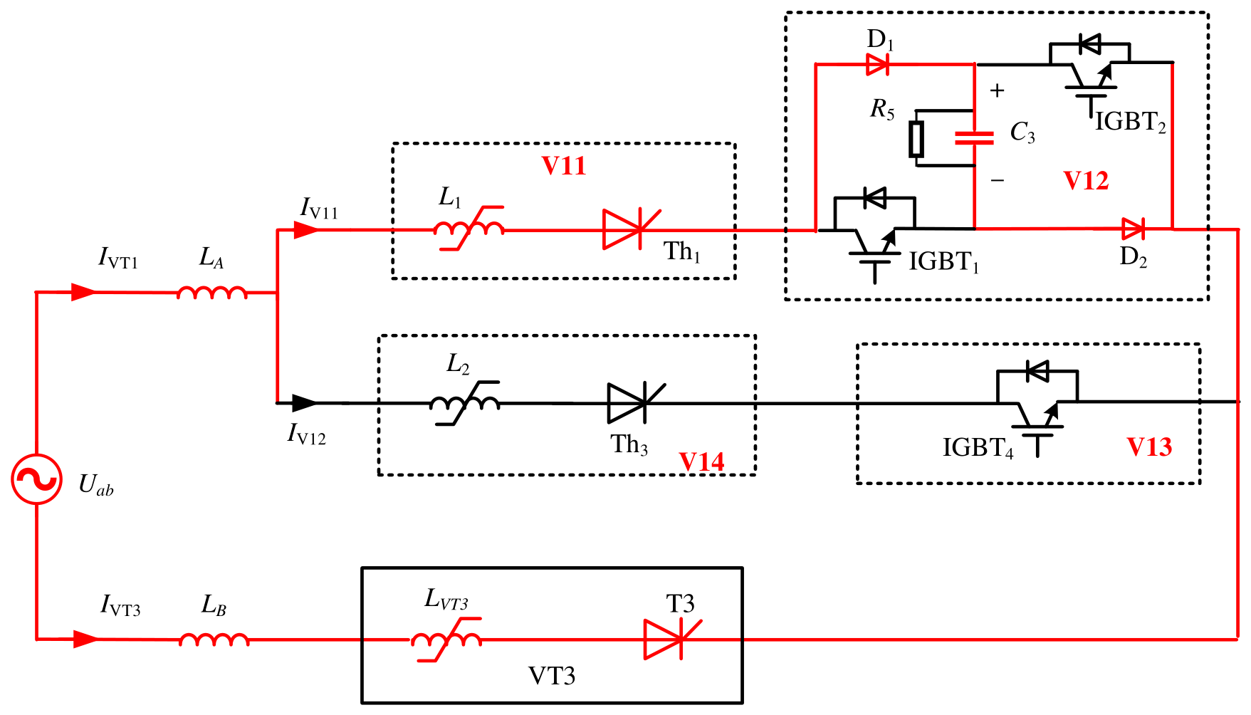
Taking the commutation process from VT1 to VT3 as an example, at the moment VT1-V12 turns off, the pre-conducting valve VT3 has already been turned on. Before the VT3 transfer branch conducts, the equivalent circuit diagram is shown in
Figure 5. At this stage, the voltage relationships in the circuit are as follows:
Here,
Uc denotes the capacitor voltage across the V12 H-bridge. Let
and
, then it follows that:
The line voltage on the valve side of the converter transformer is:
According to Kirchhoff’s Current Law:
For the VT1 main branch, the V12 capacitor current is:
By substituting Equations (4)–(6) into Equation (3), one obtains:
Applying the Laplace transform to Equation (7) and rearranging the terms gives:
Since the DC current remains constant at the moment T1/T2 turns off, and the capacitor starts charging from 0 kV, the following conditions hold:
Substituting Equations (9) and (10) into Equation (8) results in:
As shown in Equation (11), the capacitor voltage (Uc) is a function of the capacitance (C), the converter bus line voltage (), the equivalent system commutation inductance (), the DC current (), the inverter-side firing angle (), and the commutation time (t).
To investigate the voltage stress on V12 under extreme operating conditions, Equation (11) was solved using MATLAB R2021a. In this analysis, the inverter-side firing angle is assumed to be 142° [
25], and the RMS line-to-line voltage on the valve side of the converter transformer is 160 kV.
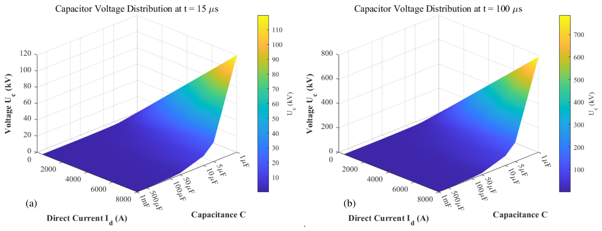
Figure 6a,b illustrate the relationship between capacitor voltage and capacitance at 15 μs and 100 μs after V12 turn-off under various current levels. It is observed that the capacitor voltage increases as the capacitance decreases or the turn-off current rises. Furthermore, the voltage magnitudes in
Figure 6b are significantly higher than those in
Figure 6a, which is attributed to the continuous accumulation of capacitor voltage over the charging duration.
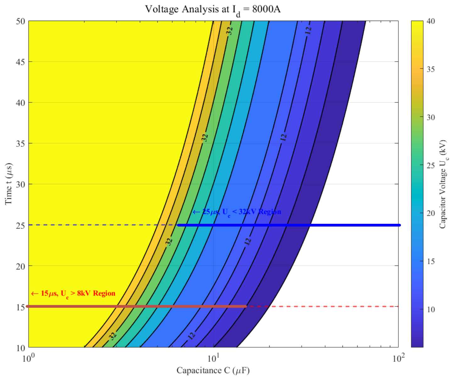
Considering the constraints of the V12 capacitance, to ensure reliable current commutation between the main and auxiliary branches, the capacitor voltage must be sufficient to establish the on-state voltage drop for the auxiliary branch thyristors (V14) at 15 μs after the turn-off of T1/T2. This voltage is calculated as 8000 V in total, based on 100 V per level across 80 levels of V14. Furthermore, taking into account the 10 μs turn-on delay of the thyristors, the peak capacitor voltage must remain below the device’s voltage withstand limit (calculated as 32 kV in this study, based on 4 kV per level across 8 levels of V12) under the most severe fault turn-off conditions.
To investigate the voltage stress on V12 under extreme operating conditions, the relationship between capacitor voltage and capacitance at various time intervals after V12 turns off an 8 kA current is detailed in
Figure 7. It can be observed that with a capacitance range of 6.5–15 μF, the capacitor voltage reaches 8 kV within 15 μs of V12 turn-off, satisfying the necessary condition for commutation between the main and auxiliary branches. Additionally, considering the 10 μs turn-on delay of the V14 thyristor, the capacitor voltage does not exceed 32 kV at 25 μs after V12 turn-off, providing a sufficient safety margin. Consequently, based on an 8-level series design for the V12 sub-valve, the capacitance for each level is determined to be 52–120 μF.
To further verify the accuracy of the range specified in
Figure 7, a theoretical analysis was conducted to determine the required turn-off current for various capacitance values. This analysis assumes a target charging voltage of 2000 V—the threshold required for V12 gate-drive energy harvesting—during the current turn-off process. During the charging phase (on the order of 100 μs), the charging current
i(t) is assumed to exhibit a linear decay characteristic, expressed as:
where
k is the current slope related to the commutation reactance. In this study,
k is assumed to be a constant, which is determined from the numerical simulation results detailed later in
Section 5. According to the principle of charge conservation, the total charge Q accumulated by the capacitor is given by:
where
tf is charging time. By substituting (11) into (12) and considering the boundary condition
i(t
f) = 0, the following relationship is obtained:
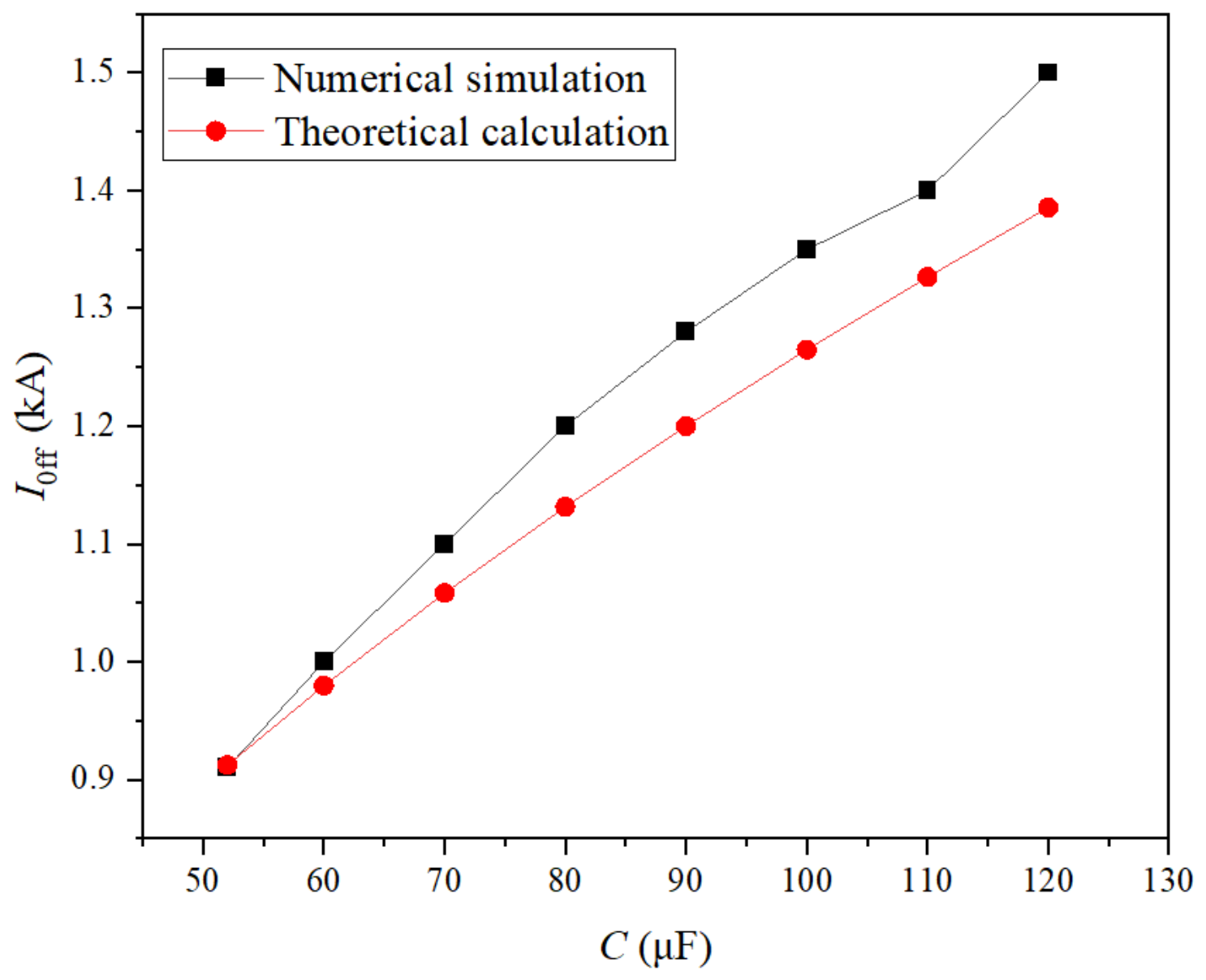
As indicated by Equation (14), the capacitor voltage after V12 turn-off depends solely on the capacitance value and is independent of the charging duration. To validate this analysis, numerical simulations were performed in PSCAD with capacitance ranging from 52 μF to 120 μF, as shown in
Figure 8. It is observed that as the capacitance increases, achieving a 2 kV post-turn-off voltage across V12 requires an earlier turn-off time and a corresponding increase in the turn-off current
. For instance, the simulation results show that for capacitances of 52 μF, 90 μF, and 120 μF, the required turn-off currents are 0.9 kA, 1.3 kA, and 1.5 kA, respectively. These findings further demonstrate that larger capacitance values are detrimental to the energy-harvesting process of V12 under low-power operating conditions. The theoretical derivations show excellent agreement with the numerical simulations at lower capacitance levels. However, a slight discrepancy arises at higher capacitance values. This is attributed to the increased current shunting through the auxiliary branches when the turn-off current is high.
5. Numerical Simulation and Analysis
Numerical simulations were conducted using PSCAD/EMTDC to evaluate the performance of the CLCC converter valve under normal commutation, single-phase ground fault, and capacitor short-circuit scenarios. The operational timeline is defined as follows:
- (1)
At 0.05 s: The converter valve is de-blocked to initiate operation.
- (2)
At 0.3 s: A single-phase-to-ground fault is applied to the AC grid side, while the H-CLCC operational mode is adjusted to forced commutation mode.
- (3)
At 0.6 s: A capacitor short-circuit fault occurs within a single-stage H-bridge of V12. Consequently, the two adjacent cascaded H-bridge stages exit the CLCC mode to maintain system integrity.
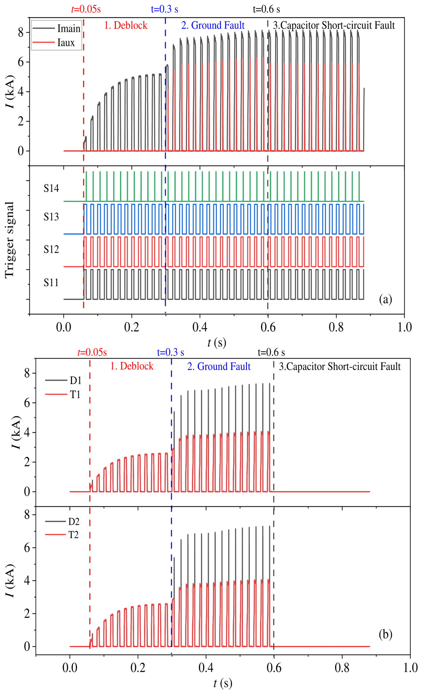
In this study, the simulation is conducted based on a HVDC system with a nominal current of 5 kA and a single-valve DC voltage of 200 kV. The firing angle is configured at 142°, and the simulated contingency is a single-phase-to-ground fault occurring on phase B of the AC grid side. Furthermore, the H-bridge capacitance (C3) is configured at 90 μF, with a measured turn-off current of 1.3 kA during the steady-state natural commutation process. The dynamic responses of the main and auxiliary branch currents, along with their respective gate triggering signals, are illustrated in
Figure 9a. Furthermore, the transient current distributions within the H-bridge assembly are depicted in
Figure 9b. It can be observed that the current trajectories and magnitudes exhibit distinct characteristics across the three aforementioned operational phases. A comprehensive analysis of these current profiles and the underlying physical mechanisms for each stage is presented in the following subsections.
5.1. Normal Conditions
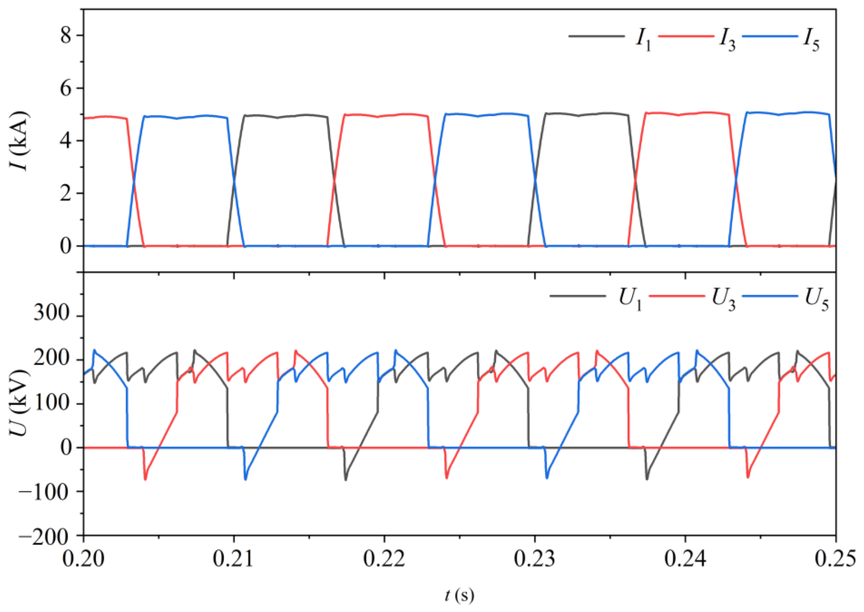
The transient voltage and current profiles of the VT1-VT3-VT5 bridge arms during the natural commutation process are illustrated in
Figure 10. It can be seen that the maximum current across each sub-valve is 5 kA, while the total arm voltage reaches approximately 200 kV.
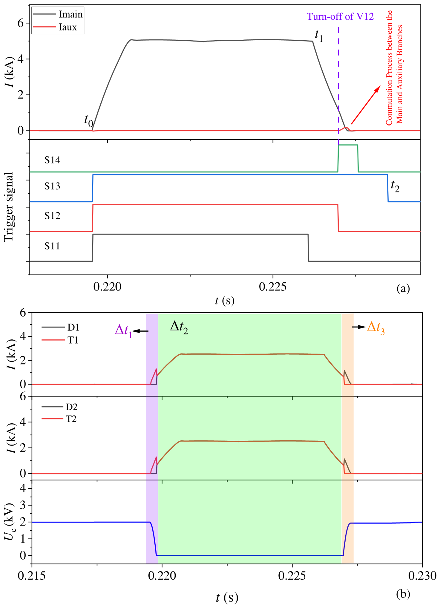
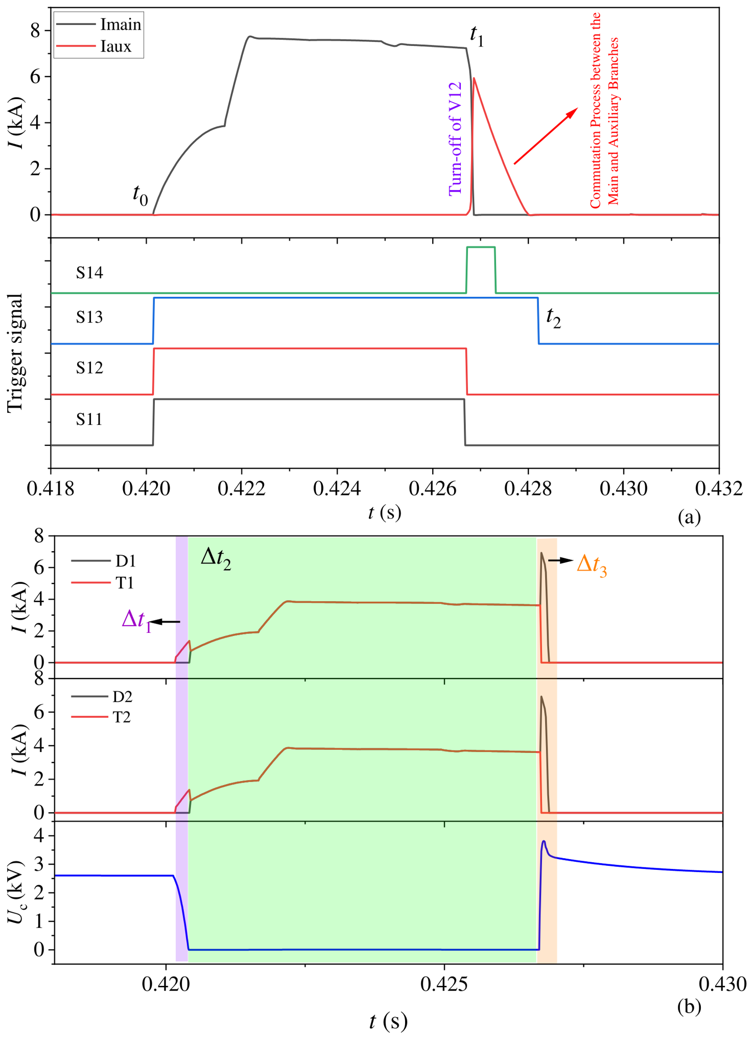
Figure 11a depicts the branch currents alongside the control pulse sequences for both the main and auxiliary paths. As observed, sub-valves V11, V12, and V13 are triggered simultaneously at t
0. Since V14 remains in a blocked state, the entire arm current is initially routed through the main branch. Following a 120° conduction interval, the arm current begins to ramp down at t1. Once the current decays to 1.3 kA, V12 is commanded to turn off, while V14 is concurrently triggered to conduct. This sequence initiates the H-bridge capacitor charging and the subsequent commutation process for main and auxiliary paths. Precisely 1.5 ms after the turn-off of V12, a turn-off signal is issued to V13, thereby achieving Zero-Current switching.
Figure 11b illustrates the transient currents flowing through the H-bridge IGBTs (T
1 and T
2) and diodes (D
1 and D
2). It can be observed that the current flow during the arm conduction stage is divided into three distinct phases. In the first phase (Δt
1), during the arm turn-on process, the current flows through T
1 and T
2. This stage represents the reverse charging process of the H-bridge capacitor, during which the capacitor voltage decreases; the corresponding current path is detailed in
Figure 4a. Once the capacitor voltage drops to zero, the current flow enters the second phase. At this point, the current is equally shared between the two internal parallel paths of the H-bridge (T
1-D
2 and D
1-T
2), with each path carrying half of the total current, as shown in
Figure 4b. This state is maintained until the arm commutation begins. When the arm current decreases to the preset turn-off threshold of V12, T1 and T2 are turned off, and the current enters the third phase. In this phase, the current flows through the D
1-C
3-D
2 path to charge C
3, as illustrated in
Figure 4c. The accumulation of voltage on C
3 serves two primary purposes: establishing the necessary forward voltage drop for the conduction of V14 and providing power for the energy-harvesting supply of V12.
5.2. Fault Conditions
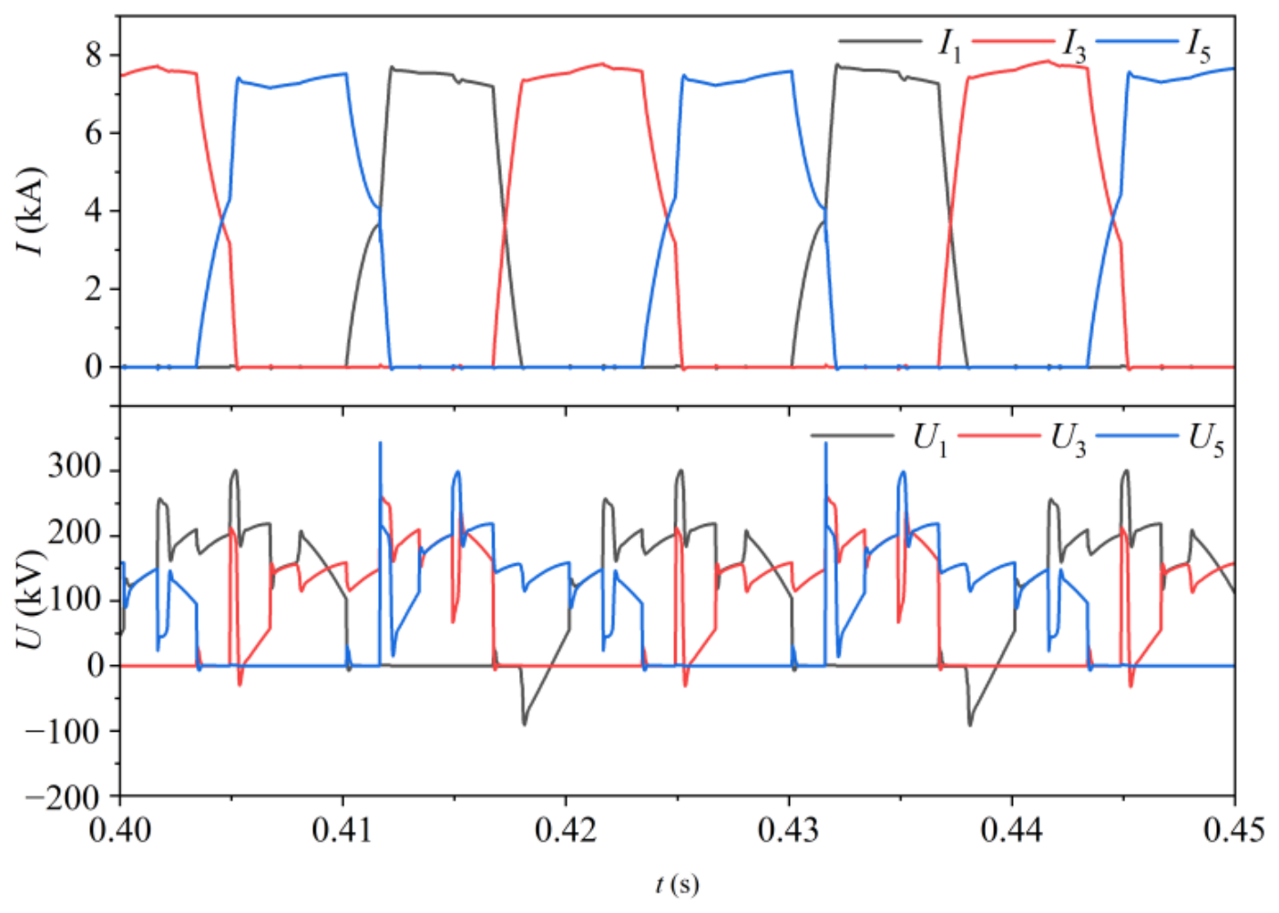
To investigate the immunity of the CLCC converter valve against commutation failure under fault conditions, a single-phase-to-ground fault is applied on the AC grid side in the numerical simulation. The resulting peak fault current reaches approximately 8 kA, with the simulation results presented in
Figure 12. It can be observed that despite the fault current magnitude, the CLCC valve successfully completes the commutation process, ensuring stable system operation. This validates the robust fault-ride-through capability of the H-CLCC converter valve. The underlying principle of the H-CLCC in mitigating commutation failure is consistent with that of the conventional series-connected CLCC valve, as detailed in references [
19,
20,
21].
Figure 13 illustrates the branch currents and control pulse sequences for both the main and auxiliary paths. The current flow under fault conditions is also divided into three stages, which is consistent with the natural commutation process. However, compared to natural commutation, several key differences are observed: (1) due to the ground fault, the current magnitudes in all branches increase significantly; (2) to guarantee successful commutation, the turn-off timing of V12 is advanced to the falling edge of the V11 conduction sequence; (3) owing to the increased turn-off current, the voltage across capacitor C3 rises more rapidly during the V12 turn-off process and is eventually clamped at approximately 3.8 kV by the surge arrester residual voltage. Furthermore, the commutation between the main and auxiliary branches becomes more pronounced, with the auxiliary branch current reaching a peak of 6 kA, compared to approximately 1 kA during natural commutation.
5.3. Device-Failure Conditions
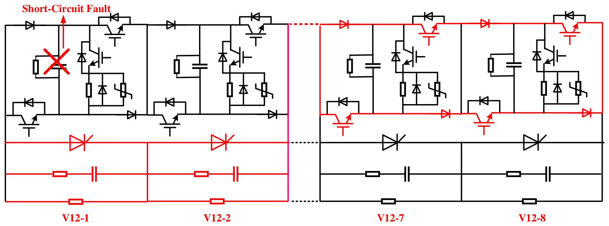
The proposed H-CLCC valve features a self-healing capability that allows specific H-bridge sub-modules to exit CLCC mode and revert to LCC operation in the event of device failure. For instance, upon an IGBT communication/breakdown failure or a capacitor flashover/breakdown, the faulty stage and its adjacent stage are simultaneously withdrawn from CLCC mode—i.e., the IGBTs are blocked and the H-bridge is bypassed—to ensure stable system operation. In such cases, the arm current of the faulty stage is diverted through the bypass thyristor. Once activated, the trigger timing of the bypass thyristor aligns with that of V11, thereby maintaining normal arm operation. Taking a capacitor short-circuit fault as an example (as shown in
Figure 14), when a short-circuit occurs in the V12-1 capacitor, both the V12-1 and V12-2 H-bridge stages exit operation with all IGBTs blocked. The current for these two stages flows through the bypass thyristor valve while the remaining H-bridges continue normal operation.
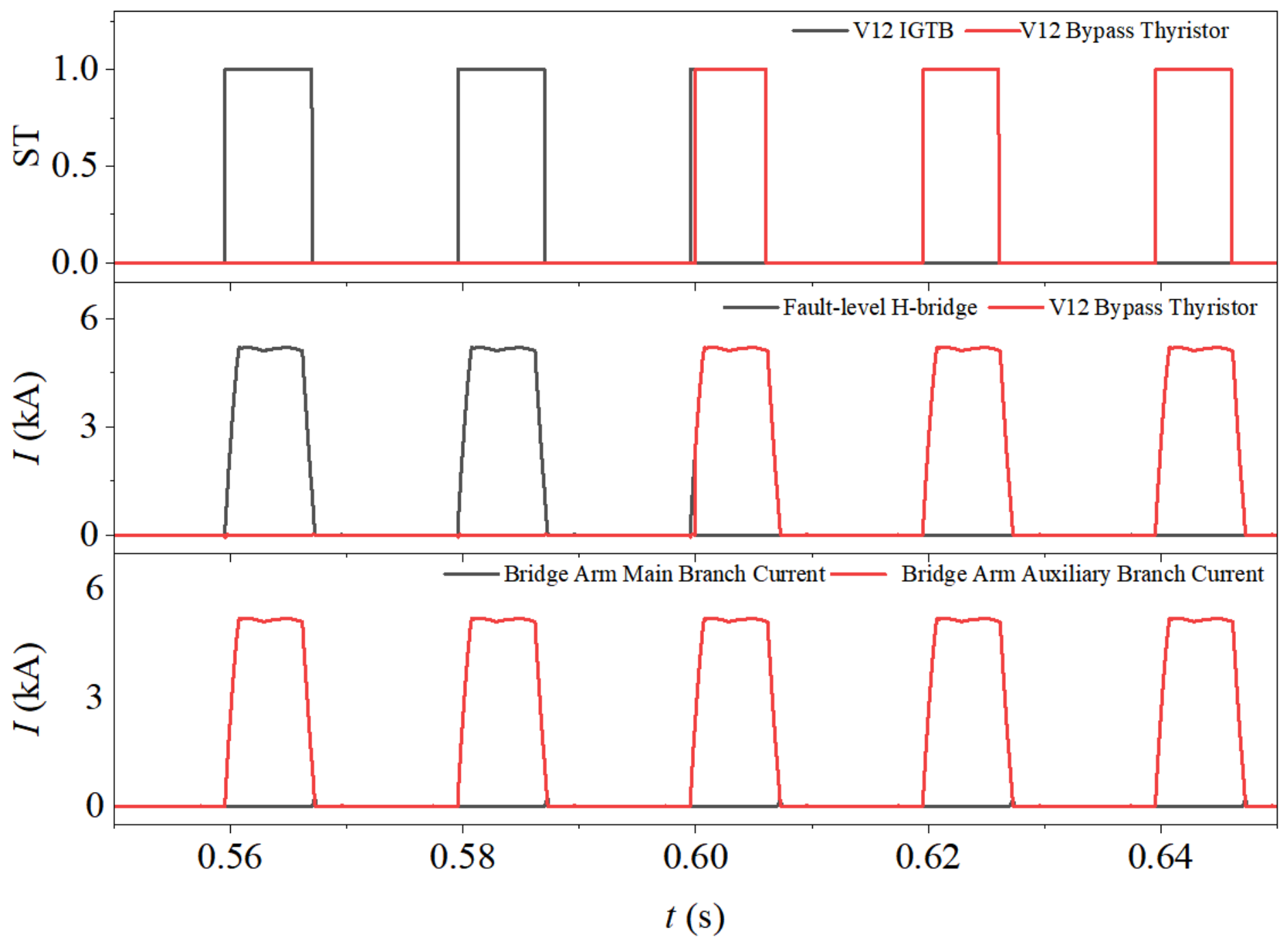
Figure 15 illustrates the trigger timings for the IGBTs and thyristors of the faulty stage, along with the main and auxiliary branch currents. It can be observed that at the moment of failure, the H-bridge current is rapidly diverted to the bypass thyristor valve; in subsequent cycles, the arm current consistently flows through the bypass path. Furthermore, since the remaining healthy V12 H-bridge stages continue to operate in CLCC mode, the current transfer between the main and auxiliary branches proceeds normally. Consequently, the converter valve retains its immunity against commutation failure.
To evaluate the operational boundaries and parameter adaptability of the proposed H-CLCC valve, sensitivity analyses regarding capacitance variations and module stage counts are conducted.
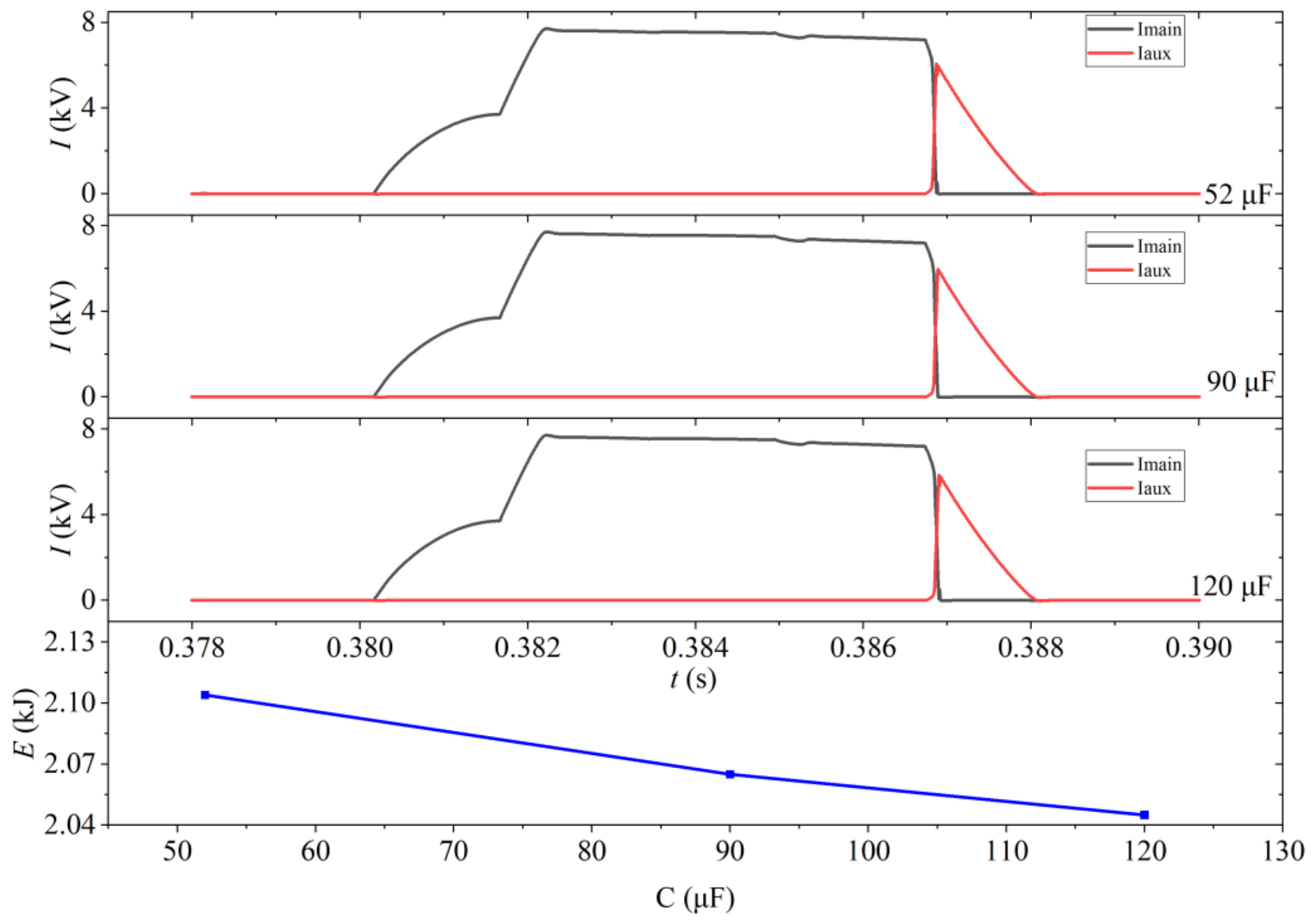
Figure 16 illustrates the transient current transfer profiles (
Imain and
Iaux) and MOV energy dissipation (
E) under dynamic fault forced commutation across capacitance values of 52 µF, 90 µF, and 120 µF. As observed in
Figure 16, the main branch current is successfully interrupted and transferred to the auxiliary path in all cases, confirming that the valve maintains robust immunity against commutation failure across the entire capacitance design window. Furthermore, increasing the capacitance from 52 µF to 120 µF reduces the peak energy dissipation absorbed by the MOV arrester from 2.10 kJ to 2.04 kJ. This benefit arises because a larger H-bridge capacitance allows sub-valve V12 to absorb a greater share of dynamic transient energy during the charging process, thereby alleviating thermal stress on the energy-dissipation branch. It is worth pointing out that although a larger capacitance reduces MOV energy stress, an excessively large capacitance value slows down the rate of voltage build-up across sub-valve V12 during normal operation and increases steady-state power losses; thus, the design range of 52–120 µF is specified based on the analytical trade-off established in
Section 4. Additionally, active forced commutation is strictly preserved across dynamic fault conditions provided the cascaded stage count N remains above N_min to fulfill the BOD triggering voltage requirement of V14.
Beyond fulfilling dynamic commutation requirements, the capacitor optimization framework directly supports long-term valve reliability and semiconductor device stress management. In high-power UHVDC applications, power capacitors experience gradual capacitance degradation over multi-year service lives. To compensate for parameter drift, real-time capacitor voltage monitoring is integrated into the valve control strategy. Upon detecting capacitance reduction, the control system adaptively delays the turn-off timing of sub-valve V12 to dynamically reduce the turn-off current, ensuring that the capacitor voltage reliably reaches the necessary thresholds without exceeding device safety margins. Furthermore, limiting voltage rise rates (dv/dt) via optimal capacitance selection and adaptive current control mitigates dynamic switching losses and junction temperature fluctuations in power semiconductors. Minimizing such thermal stress directly prevents bond-wire fatigue and solder-layer degradation, ensuring long-term structural integrity and high operational availability for the H-CLCC valve throughout its operating lifetime.
6. Conclusions
This paper presents an in-depth investigation into the principles, topology reliability, capacitance design criteria, and operational performance of a high-reliability H-CLCC valve. By establishing a dual-path conduction mechanism within the cascaded H-bridge sub-valves, each IGBT carries only 0.5 p.u. of the rated DC current during steady-state operation, effectively breaking through the current-carrying limitations of existing power electronic devices in 5 kA-class UHVDC applications. Furthermore, the two-stage cascaded H-bridge configuration, integrated with parallel bypass thyristors, establishes a robust self-healing redundancy mechanism. Upon local submodule failures such as capacitor short-circuits, the faulty stages are smoothly bypassed to revert locally to LCC mode without interrupting main system operation or compromising overall valve availability.
To ensure optimal transient and dynamic performance, a refined Laplace-transform-based analytical model was developed, defining a capacitance design window of 52–120 µF. This range guarantees that the forward voltage required for auxiliary branch triggering is synthesized within 15 µs while strictly bounding peak voltage stress during energy harvesting. Extensive PSCAD/EMTDC numerical simulations confirm that by advancing the H-bridge turn-off timing, the proposed H-CLCC valve achieves superior immunity against commutation failure, maintaining reliable forced commutation even under severe AC single-phase-to-ground faults with peak fault currents reaching 8 kA.
To further advance the engineering implementation and theoretical framework of the proposed H-CLCC converter valve, future research will focus on three main directions. First, comprehensive hardware-in-the-loop testing and full-scale experimental validations will be conducted to evaluate controller execution latency, gate-triggering delays, and overall control system burden under diverse dynamic conditions. Second, advanced local dynamic control strategies will be explored, particularly integrating transient di/dt detection to enable adaptive, timer-based turn-off algorithms for decaying fault currents, thereby optimizing switching losses. Third, multi-parameter sensitivity analyses will be expanded to encompass a broader spectrum of complex fault scenarios—including multi-phase grounding, AC/DC hybrid faults, and varying short-circuit ratios—to fully map the performance boundaries and long-term reliability of the H-CLCC topology.




 ,
,