1. Introduction
Low-noise amplifiers (LNAs) are a fundamental building block of radiofrequency (RF) receivers, as they determine the overall sensitivity of the system by amplifying very weak input signals while introducing minimal additional noise. For this reason, the first stage of the receiver chain is typically an LNA designed to provide both high gain and a low noise figure (NF).
In recent years, advanced CMOS technologies have enabled the implementation of highly integrated RF front ends operating at microwave frequencies [
1,
2,
3]. Among these technologies, FinFET nodes have attracted significant interest due to their excellent electrostatic control, improved short-channel behavior, and high-frequency performance [
4]. Several studies have demonstrated the suitability of FinFET devices for RF and millimeter-wave integrated circuits across a wide range of applications [
5], from broadband wireless communications [
6] and sensing systems to cryogenic instrumentation, radio astronomy, high-energy physics experiments [
7], and emerging quantum-computing readout architectures [
8,
9,
10,
11]. These properties make FinFET technologies attractive candidates for implementing high-performance RF systems.
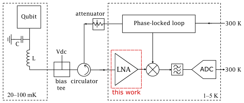
Among the emerging application domains, quantum computing represents a particularly demanding scenario for RF integrated circuits. In superconducting qubit platforms, the information encoded in the qubit state is typically read out through microwave signals in the few-GHz range. As illustrated in
Figure 1, the readout chain resembles a conventional RF receiver, where extremely weak signals must be amplified while preserving the signal-to-noise ratio. In this context, LNAs operating around the 5 GHz band at a cryogenic temperature (typically around 4 K) represent a key building block [
12,
13].
The implementation of LNAs in deeply scaled FinFET technologies presents several design challenges. In particular, the simultaneous achievement of a low NF and accurate input matching often relies on integrated inductive networks, whose practical realization becomes increasingly critical as technology nodes scale. The limited quality factor of integrated inductors, layout constraints, and parasitic effects may significantly impact the achievable RF performance and introduce non-negligible discrepancies between the theoretical and measured results [
14,
15,
16,
17]. Understanding these limitations is therefore essential for the development of high-performance RF front ends in advanced CMOS technologies.
In this work, two LNAs operating at 5 GHz were designed and experimentally characterized in 16 nm and 7 nm FinFET technologies. Both circuits employed a cascode common-source topology with inductive degeneration, but different design approaches were adopted. The first implementation followed a conventional simultaneous noise and input-matching strategy, while the second prioritized the minimum noise figure (NFmin) through an iterative electromagnetic-aware optimization procedure. The comparison focused on two practical design strategies rather than on the intrinsic performance of the two technology nodes, as the two technologies offer comparable RF front-ends. This work highlights the practical trade-offs between the matching accuracy, passive implementation losses, and achievable noise performance in advanced FinFET technologies.
2. Proposed LNA Architecture and Design Considerations
The LNAs proposed in this work use a cascode common-source topology, widely adopted in RF front-end design for its excellent performance in terms of gain, stability, and reverse isolation [
18]. In this architecture, the input transistor operates as a common-source stage, providing the main transconductance and dominating the noise performance of the amplifier, while the cascode device improves the isolation between the input and output, and increases the effective output resistance, enabling a higher voltage gain [
19,
20,
21].
Two similar structures, with slightly different design approaches, were implemented in both FinFET 16 nm and FinFET 7 nm technologies to compare the two design strategies and assess their respective advantages and limitations.
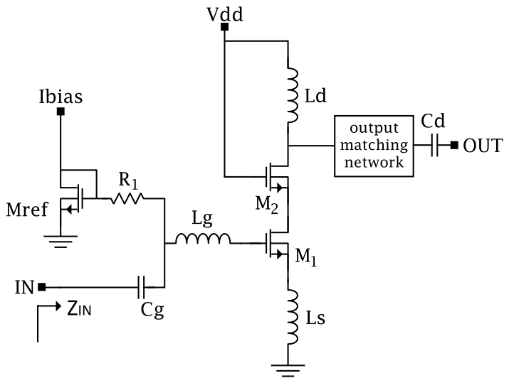
The schematic of the proposed LNA is shown in
Figure 2. The bias of the main transistor
is provided by a current mirror, while the cascode
is biased by connecting its gate to
. The bias resistor
was chosen to be sufficiently large (
) to provide the required DC gate bias while effectively isolating the RF signal from the bias network. Although
generates thermal noise, its contribution to the overall NF is negligible because the large resistance presents a very high impedance at RF, resulting in the minimal coupling of its noise to the input transistor. At the output side, the inductor
at the drain terminal of
is used as a DC feed. At the same time, its finite impedance at the operating frequency is used as part of the output-matching network to achieve the desired output impedance.
Regarding the input network, to simultaneously achieve low noise and proper input matching, a matching network consisting of source degeneration inductance (
) and gate inductance (
) was introduced at the input of the common-source stage. Considering the small-signal model of the input transistor and neglecting higher-order parasitic elements, the input impedance of the stage can be approximated as [
19]:
where
is the gate-source capacitance and
is the transition angular frequency. From this expression, it can be observed that the source inductance introduces a real component in the input impedance equal to
, which is used to match the input resistance to the
RF source impedance. At the same time, the imaginary part of the input impedance can be compensated for by properly selecting the gate inductance so that it resonates with the device’s intrinsic gate capacitance at the selected operating frequency.
Since the noise and input-matching properties of the LNA are largely determined by the electrical characteristics of the input transistor, this was first analyzed under the bias conditions used in the amplifier design. In particular, at the minimum channel length, the 16 nm technology provides a higher current per effective width and a higher transconductance (
) than its 7 nm counterpart, where the effective width is defined as:
Overall, the two FinFET processes showed very similar device characteristics. In both cases, the transition frequency extracted from the simulation was around 300 GHz, while the gate–source capacitance was on the order of a few tens of femtofarad. Only minor differences were observed, with the 7 nm node exhibiting a slightly higher and a slightly lower .
Using the device parameters extracted from PDK simulations and according to Equation (
1), the required inductance values were estimated to be approximately
and
, which are not practically realizable as on-chip passive components. In particular, a source inductance of a few picohenry would make the design extremely sensitive to layout parasitic effects and process variations, while a gate inductance of several tens of nanohenry would require an unrealistically large on-chip spiral inductor, far beyond the area and quality factor limits achievable in FinFET processes. Therefore, a different matching strategy must be adopted to obtain practical inductance values compatible with integrated implementation. The solution adopted in this work was to artificially increase the input capacitance by
by adding a metal–oxide–metal (MOM) capacitor at the input side, obtaining a “capacitance-augmented transistor”. The value of the additional capacitance (
) was chosen to make the values of
and
more feasible in integrated solutions. Equation (
1) becomes
where the last term is reduced as a consequence of the additional
. Since the
can be approximated as
and the external MOM capacitor adds to the intrinsic input capacitance while leaving
essentially unchanged, the effective
of the “capacitance-augmented transistor” becomes
Therefore,
showing that the effective
is reduced in approximately inverse proportion to the increase in the input capacitance. In particular, in this work, the effective
of the “capacitance-augmented transistor” decreased from approximately
to about
[
21]. In this way,
was increased to around
and
was decreased to around
, enabling more practical passive implementations.
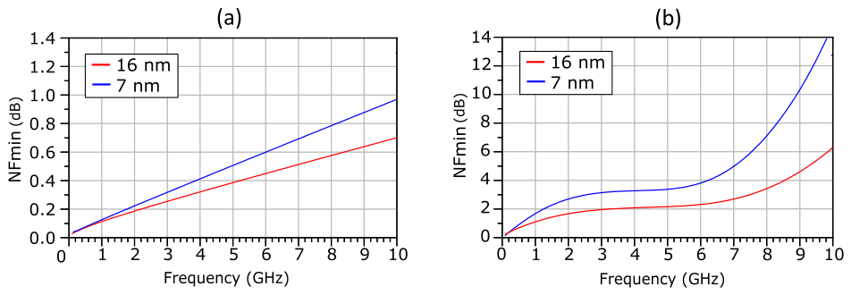
The intrinsic noise performance of the input device can be evaluated through conventional noise parameters such as the NF. To evaluate the intrinsic noise performance of the two technology nodes, the NFmin of the two devices in common-source configuration is reported in
Figure 3a. In both cases, the maximum number of fingers (32) and fins (20) was adopted at the minimum channel length. The maximum nominal voltage was applied, meaning that the 16 nm FinFET was biased with a higher current. The values obtained from the simulations represent only a first-order estimation and correspond to the theoretical limit that it is difficult to achieve in practice. Indeed, the minimum NF condition occurs under a strong input impedance mismatch, which is undesirable from a practical RF design standpoint. Moreover, the analysis considered only a single non-stabilized transistor, while any additional elements introduced to improve the stability or matching inevitably degrade the NF.
When an additional capacitance of
is inserted between the gate and source of
, and the source and gate inductances are chosen according to Equation (
3), the NFmin in the two configurations becomes the one reported in
Figure 3b.
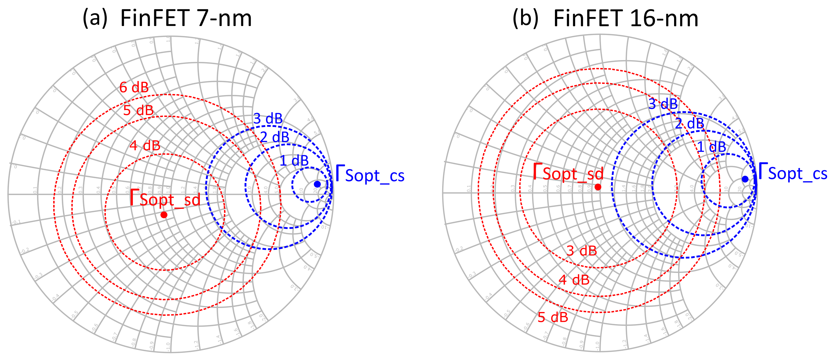
Figure 4 shows the noise circles of the 16 nm and 7 nm transistors with a 1 dB spacing, together with
, i.e., the optimal source reflection coefficient that minimizes the NF of the transistor. In particular,
is reported for both the simple common-source topology (
) and the source-degenerated capacitance-augmented common-source topology (
). In the latter case, the optimum is significantly closer to the center of the Smith chart, indicating that a better trade-off between the NF and the input matching can be achieved.
3. Implementation and Results of the 7 nm LNA
Based on these considerations, an LNA in 7 nm technology was designed to achieve simultaneous input and noise matching. To further facilitate the input matching, the channel length of the main transistor was increased to
. This choice reduced the
and increased the
, thereby relaxing the matching requirements and enabling more practical values for the input inductors, as discussed in the previous section. Referring to
Figure 2, both transistors
and
were implemented with 32 fingers and 20 fins. The source and gate inductors were selected to be 400 pH and 4.2 nH, respectively, according to Equation (
3), while the drain inductor was set to 2 nH to provide enough isolation for the RF signal from the supply.
The design was fabricated and the LNA was experimentally validated through room-temperature S-parameter and noise measurements. The supply voltage was set to 750 mV and the total power consumption of the proposed LNA was
, while the occupied area was
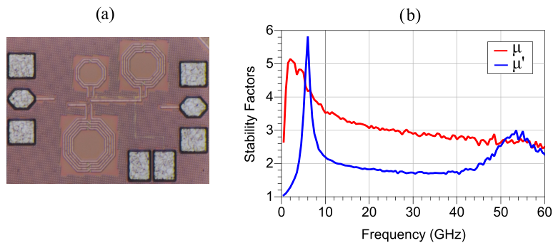
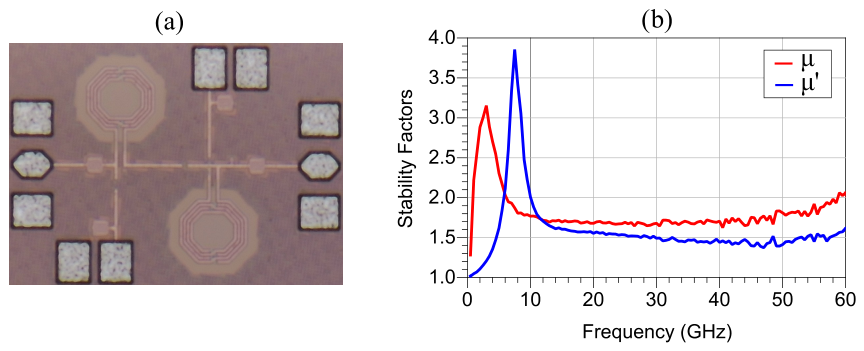
. A micrograph of the circuit is shown in
Figure 5a. The S-parameter measurements were performed using a vector network analyzer (VNA) capable of a continuous sweep from 70 kHz to 220 GHz (Antitsu MS4647B, (Anritsu Corporation, Atsugi, Japan)); a high-resolution (2
V; 10 fA) and high-accuracy (V: 0.01%, I: 0.1%) semiconductor analyzer (Keysight B1500, (Keysight Technologies, Santa Rosa, CA, USA)) for providing the bias for the DUT; and a custom software based on NI LabVIEW (2024 Q1) for instrument control and data acquisition.
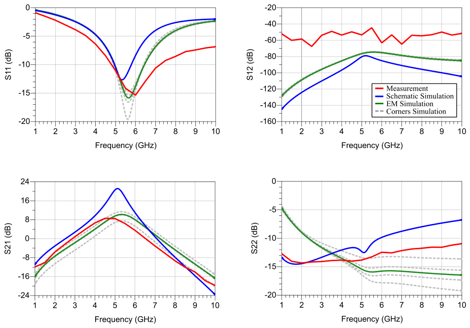
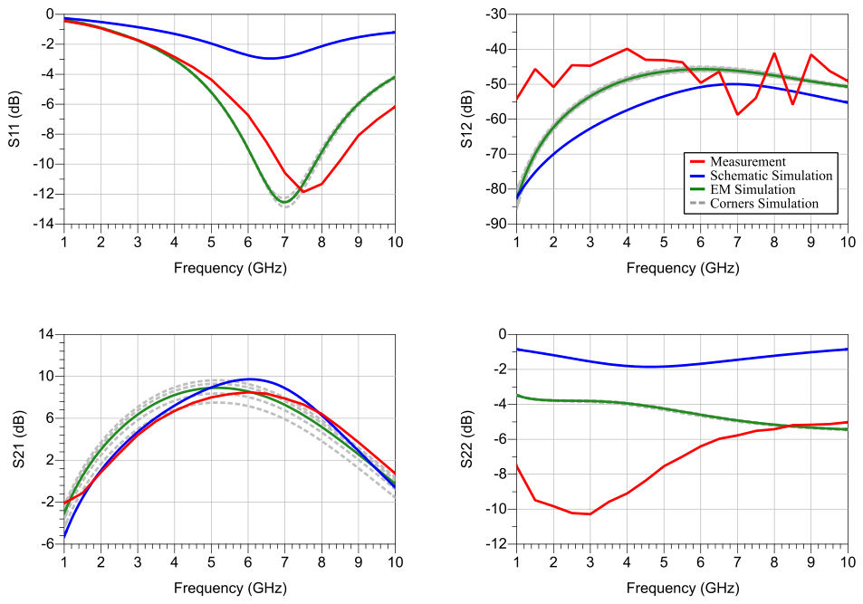
The measured results, reported in
Figure 6, confirm that the design was centered around the target frequency of 5 GHz.
Figure 6 also compares the measurements with schematic-level simulations (typical corner) and post-layout EM simulations. EM simulations were carried out using Cadence EMX. The on-chip inductors and critical RF interconnects were EM-extracted using the foundry substrate model while the active devices were simulated using the foundry PDK models across the process corners. Single-ended lumped ports referenced to the ground were adopted for the EM simulations. Overall, a good agreement was observed between the simulations and measurements. The measured input matching closely followed the predicted response, while the output matching agreed well with the schematic-level simulations, with a slight degradation at lower frequencies in the EM results. The EM simulations also predicted the gain reduction caused by passive implementation losses, resulting in a lower peak gain than the schematic-level simulations. The measured gain closely matched the EM prediction, with only a slight frequency shift. Both the simulations and the measurements were performed at the same bias current in the main amplifier branch. The amplifier achieved a maximum gain (
in
Figure 6) of 8.5 dB, a 3 dB bandwidth extending from 3.8 GHz to 5.6 GHz, and satisfactory input matching across the operating band, with
dB at 5 GHz. Output matching was also achieved using a pMOS buffer, providing an output impedance of approximately
with a low current consumption and an output return loss of
dB at 5 GHz.
The measured
and
stability factors up to 60 GHz are shown in
Figure 5b, indicating that the circuit is unconditionally stable over a wide frequency range.
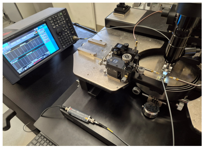
The NF at room temperature was measured using a 26.5 GHz EXA N9010B spectrum analyzer from Keysight equipped with the NF application, together with an external Keysight 346C noise source [
22]. The on-wafer measurements were carried out while accounting for the losses introduced by the cables and RF probes via the noise table feature, which can be properly configured within the instrument. A photograph of the experimental setup is reported in
Figure 7.
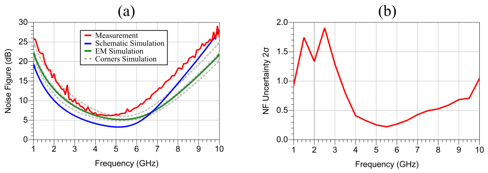
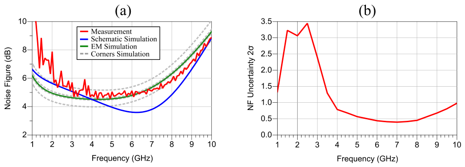
As shown in
Figure 8a, the measured NF reached a minimum value of 5.8 dB in the 4.5–5 GHz frequency range, which corresponds to the intended operating band. However, this value is higher than the one predicted by the simulations under typical-corner conditions. The results suggest that passive losses associated with the integrated inductors and critical RF interconnection paths significantly affect the achievable NF in these deeply scaled FinFET technologies. In particular, implementing inductors with a sufficiently high-quality factor is challenging because the available metal width is strongly constrained by technology design rules.
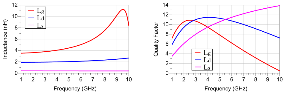
The EM simulation results of the three adopted inductors are shown in
Figure 9, while their main characteristics are summarized in
Table 1. The gate inductor (Lg) exhibited a self-resonant frequency of 9.4 GHz, whereas the self-resonant frequencies of Ld and Ls were significantly higher. Moreover, the quality factor of Lg at 5 GHz was approximately 8, while those of Ld and Ls exceeded 10. Finally, the series resistance Rs is also reported.
Moreover, additional degradation mechanisms may arise from layout-dependent effects that are difficult to accurately capture through electromagnetic simulations alone. In particular, the metal filling structures required to satisfy local density rules may further reduce the effective quality factor of the inductors. Finally, although the active core occupies a very compact area, the large passive components increase the overall layout dimensions, introducing additional parasitic resistive contributions due to interconnections and metal routing. These effects collectively contribute to the measured NF degradation.
Figure 8b also includes the noise figure measurement uncertainty, calculated using the Keysight Noise Figure Uncertainty Calculator. The reported uncertainty corresponds to the
uncertainty obtained by considering the user-defined calibration (User Cal).
4. Implementation and Results of the 16 nm LNA
Since the measured results of the 7 nm implementation indicate that passive losses strongly affect the overall noise performance, a different approach was adopted for the 16 nm design. During the design phase, the primary focus was on minimizing the NF rather than enforcing simultaneous input matching.
Therefore, the design procedure followed an iterative electromagnetic-aware optimization approach. In particular, the EM models included on-chip inductors, input capacitances, and interconnection parasitic elements, enabling a more realistic evaluation of the overall RF behavior of the circuit.
Through this iterative optimization procedure, different configurations were explored in order to identify a suitable trade-off between the noise performance and the circuit complexity. In particular, it was observed that a good compromise can be achieved by removing the source-degeneration inductor and implementing a single gate inductor of 2 nH. This solution allows the circuit to maintain a relatively low NF while keeping the passive network simple and limiting the additional parasitic effects introduced by large on-chip inductors. Referring to
Figure 2, both transistors
and
were implemented with 32 fingers and 20 fins, while the channel length was fixed to 16 nm. The drain inductor was set to 2 nH. The supply voltage was set to 800 mV and the total power consumption of the proposed LNA was
, while the occupied area was
. A micrograph of the circuit is shown in
Figure 10a.
The design was experimentally validated at room temperature using the same setup adopted for the 7 nm LNA.
Figure 10b shows that the proposed LNA was stable over a wide frequency range. The S-parameter measurements, reported in
Figure 11, show that
reached a maximum value of 8 dB at 6 GHz and exhibited a 3 dB bandwidth extending from 3.4 GHz to 8.4 GHz. The results showed a good agreement between the measurements and the EM simulations for both the forward gain (
) and the input reflection coefficient (
). A larger discrepancy was instead observed for the output reflection coefficient (
) at lower frequencies, where the EM simulations do not fully reproduce the measured response. However, since the iterative process based on EM simulations was primarily focused on minimizing the NF, neither the input nor the output matching was centered at the operating frequency, resulting in
and
values of −4.1 dB and −7.2 dB, respectively, at 5 GHz. In contrast, the measured NF, reported in
Figure 12a, showed a clear improvement over the 7 nm design, and was closer to the result obtained by the EM simulation. The minimum measured NF was 4.5 dB and remained essentially flat over the 4–5 GHz frequency range.
Figure 12b also reports the
uncertainty of the noise figure measurements.
5. Practical Design Considerations for Deeply Scaled FinFET LNAs
The experimental results provide several insights into the implementation of RF LNAs in deeply scaled FinFET technologies. Although simultaneous noise and impedance matching can theoretically improve both the input return loss and the noise performance, its practical implementation often requires relatively large integrated inductors. In advanced technology nodes, these passive components may exhibit a limited quality factor and introduce additional losses that are difficult to fully capture during the design phase.
The comparison between the two implementations suggests that the degradation introduced by passive components can become comparable to, or even larger than, the expected benefit of enforcing ideal matching conditions. In the proposed designs, the simplified matching strategy adopted in the 16 nm implementation achieved a lower measured NF, despite its poorer input-matching performance. These observations highlight the importance of considering passive implementation losses as a primary design constraint when developing RF front-end circuits in deeply scaled CMOS technologies. In
Table 2, a summary of the measured results is finally reported, together with a comparison with recent FinFET-based designs operating over similar frequency ranges. The design in [
23] achieved a lower minimum NF while targeting a lower operating frequency (2.0–2.7 GHz), where the implementation of high-Q on-chip inductors could be less challenging than 5 GHz. The LNA in [
24] demonstrated an excellent performance around 4.5 GHz, suggesting that alternative design techniques not based on inductive source degeneration may be advantageous in this frequency range for scaled technologies. Finally, the topology proposed in [
20] is similar to the present work, although only cryogenic measurement results are reported, preventing a direct comparison with the room-temperature results presented here. However, the large difference in NF can give an idea of the expected benefits at cryogenic temperatures.
6. Conclusions
This work presents the design and experimental characterization of two LNAs implemented in 7 nm and 16 nm FinFET technologies and operating in the 4.0–6.0 GHz band.
The 7 nm implementation was designed to achieve simultaneous noise and input matching through source degeneration and gate inductive tuning. The measured results confirmed proper operation around the target frequency and a satisfactory matching performance, but also revealed a degradation of the NF associated with the implementation of large integrated passive components.
A different design strategy was therefore adopted for the 16 nm implementation, where the primary objective was on minimizing the NF through an iterative electromagnetic-aware optimization procedure. By simplifying the matching network and reducing the passive complexity, the measured NF improved from to approximately , despite the less accurate input matching.
The comparison between the two implemented prototypes highlights a practical trade-off between the matching accuracy and passive implementation losses in advanced FinFET technologies. For the designs presented in this work, the measured results indicated that reducing the passive losses provided a greater benefit than enforcing simultaneous noise and impedance matching. Although this observation is specific to the investigated implementations, it suggests that passive-loss minimization should be carefully considered as a design strategy for future microwave front-end circuits implemented in advanced FinFET technologies.



 ,
,