Review

AI-on-Chip Systems: A Cross-Layer Review of Architectures, Interconnects, Design Automation, and Embedded Intelligence

James C. Morriss Division of Engineering, Texas A&M University Texarkana, Texarkana, TX 75503, USA
Electronics 2026, 15(12), 2645; https://doi.org/10.3390/electronics15122645
Submission received: 2 May 2026 / Revised: 5 June 2026 / Accepted: 8 June 2026 / Published: 15 June 2026
(This article belongs to the Topic AI Agents: Progress, Architecture, and Applications)

Abstract

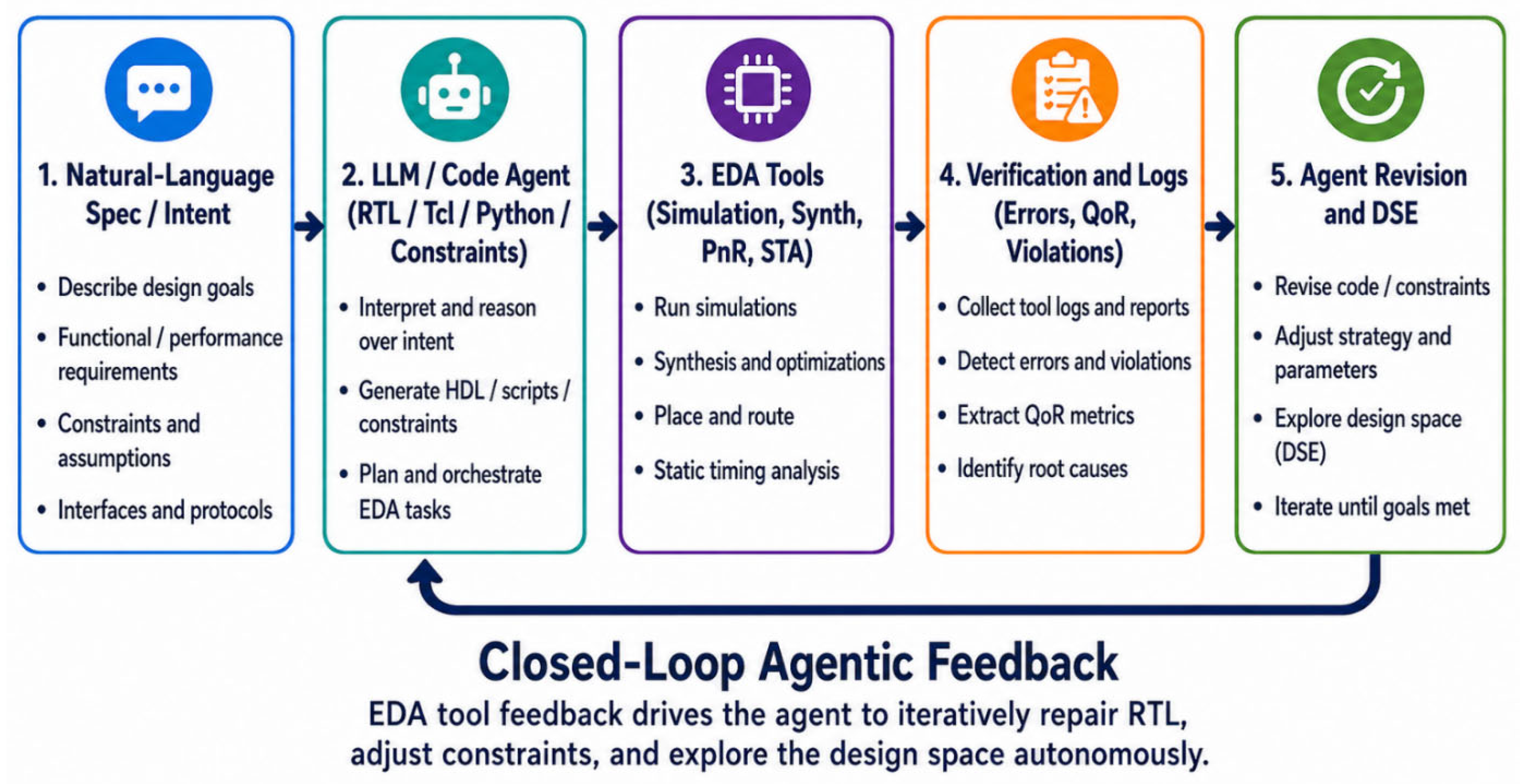
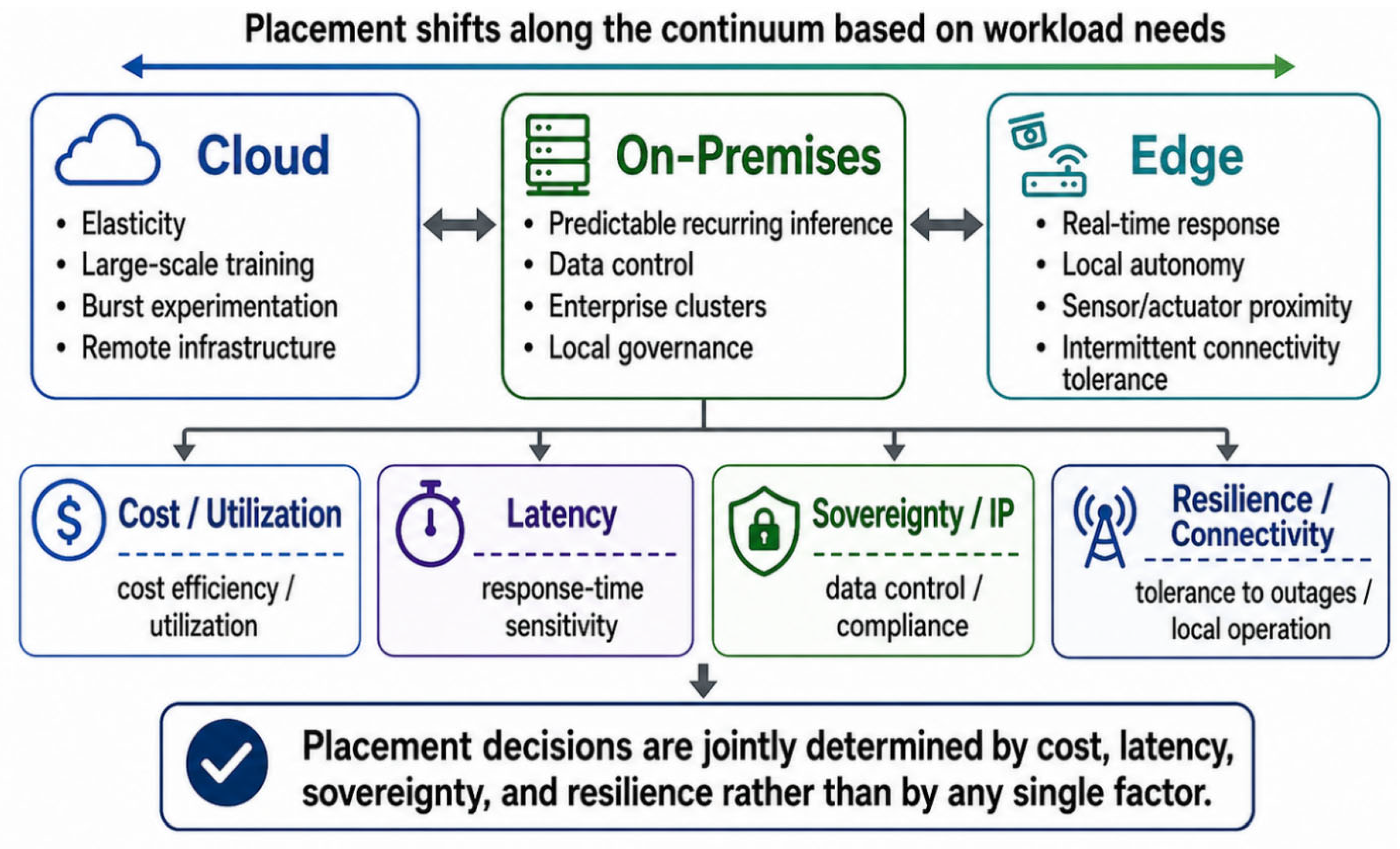
The rapid growth of artificial intelligence (AI) workloads is reshaping semiconductor design across architecture, interconnect, memory hierarchy, packaging, timing, and design automation. Rather than converging on a single hardware solution, the field is expanding into a heterogeneous ecosystem that includes data-center graphics processing units (GPUs), edge neural processing units (NPUs), and application-specific integrated circuits (ASICs), field-programmable gate array (FPGA)-based and hybrid AI system-on-chip (SoC) platforms, chiplet-enabled systems, and emerging beyond-conventional-silicon approaches such as photonic, neuromorphic, and analog in-memory processors. This paper presents a comprehensive review of AI-on-chip systems from a cross-layer perspective. It examines AI chip architectures and hardware platforms, network-on-chip (NoC) designs for AI communication patterns, and algorithm–hardware co-design methods for model acceleration, including compression, quantization, and sparsity-aware optimization. It also reviews clocking, synchronization, and clock-domain-crossing (CDC) challenges in large heterogeneous systems and chiplets, as well as manufacturing, advanced packaging, and reliability issues, including two-and-a-half-dimensional (2.5D) and three-dimensional (3D) integration, thermal and mechanical constraints, assembly quality, and long-term yield considerations. In parallel, the paper surveys the growing role of AI in chip design itself, covering machine-learning-assisted analysis, Bayesian and reinforcement-learning-based optimization, and the emerging use of large language models (LLMs) and AI agents for register-transfer level (RTL) generation, design-space exploration, and autonomous electronic design automation (EDA) workflows. Finally, it discusses beyond-silicon AI chip directions and the broader economic and industry context shaping cloud, on-premises, and edge deployment. By integrating these topics into a unified framework, this review highlights the key technological drivers, system-level tradeoffs, and future research directions that will define next-generation scalable, reliable, and energy-efficient AI-on-chip systems.

1. Introduction

Artificial intelligence (AI) has rapidly evolved from software-centric innovation to a hardware-driven paradigm that demands unprecedented computational throughput, memory bandwidth, and energy efficiency. Modern AI workloads—particularly deep neural networks (DNNs), convolutional neural networks (CNNs), and large language models (LLMs)—contain billions of parameters and require massive parallel data movement. These trends have exposed fundamental limitations of general-purpose computing architectures, especially those based on traditional central processing units (CPUs) and even graphics processing units (GPUs), where memory bottlenecks, interconnect congestion, and power constraints increasingly dominate system performance [1,2,3].
The long-standing scaling trajectory guided by Moore’s Law is no longer sufficient to sustain the exponential growth of AI model complexity. Instead, a transition toward system-level innovation—often referred to as “SysMoore”—has emerged, emphasizing heterogeneous integration, chiplet-based design, advanced packaging, and algorithm–hardware co-optimization. Recent advances demonstrate that performance improvements now rely as much on architectural reconfiguration, network-on-chip (NoC) redesign, and packaging technologies as on transistor scaling itself. For instance, architectural innovations for high-performance AI computing highlight the need for co-optimization across technology, system architecture, and algorithms. Similarly, emerging design strategies for advanced and AI chips stress coordinated advances in materials, circuits, architectures, and packaging to meet the energy and scalability demands of next-generation workloads [4,5,6,7].
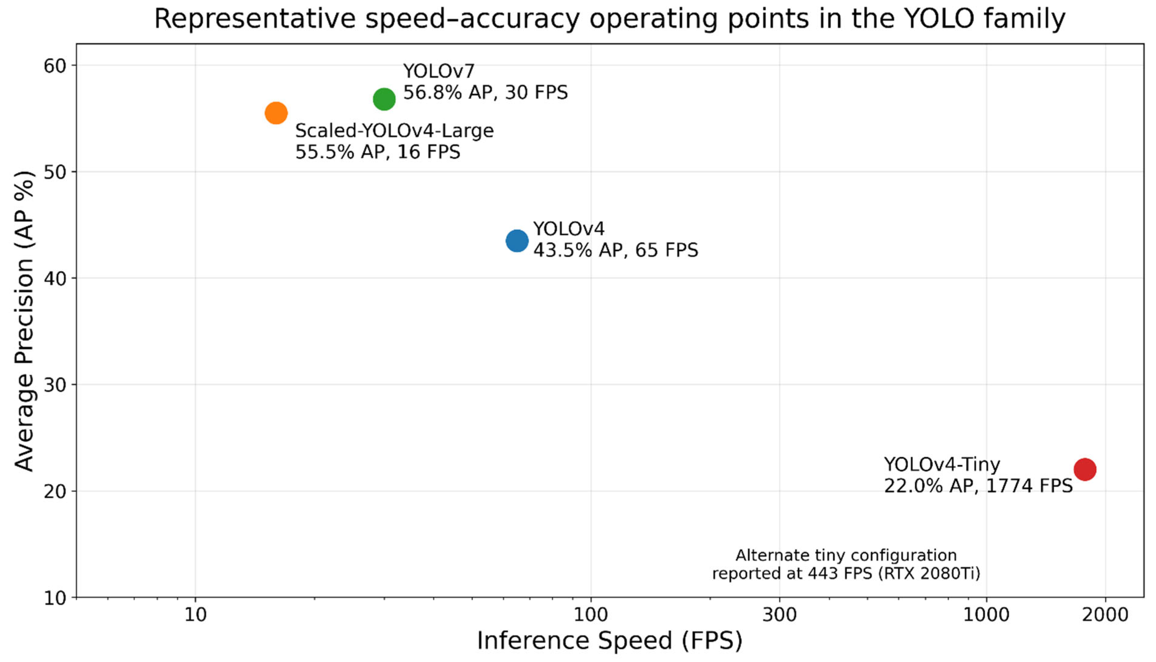
Beyond cloud-scale training accelerators, AI-on-chip solutions increasingly target edge computing scenarios where latency, power consumption, and real-time responsiveness are critical. Edge sensing, preprocessing, and inference in a unified platform. Likewise, acceleration strategies for CNN-based object detection models, including YOLOv5 optimizations on embedded AI chips, illustrate the importance of quantization, pruning, and heterogeneous acceleration in constrained hardware environments [6,8,9,10,11,12,13,14].
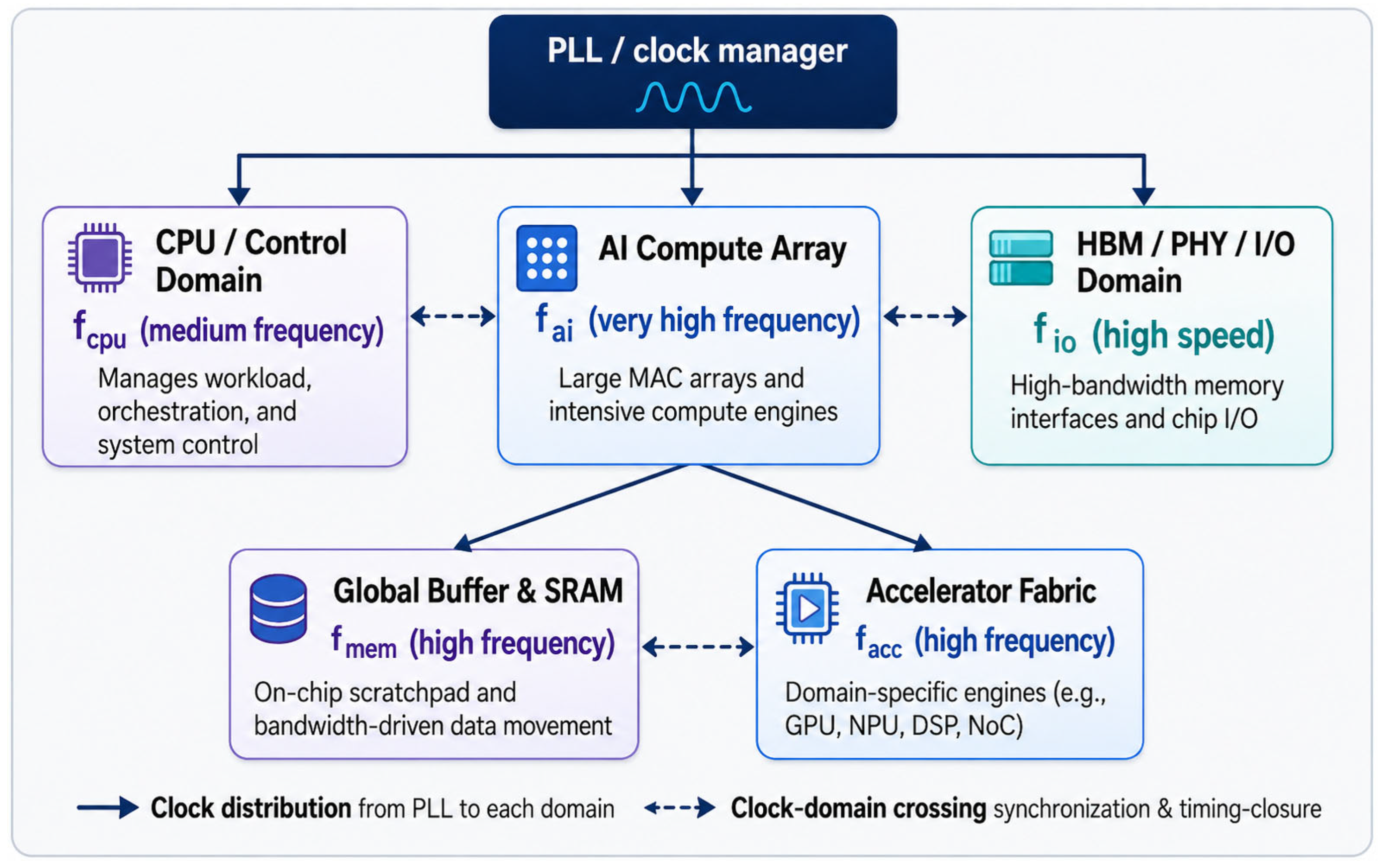
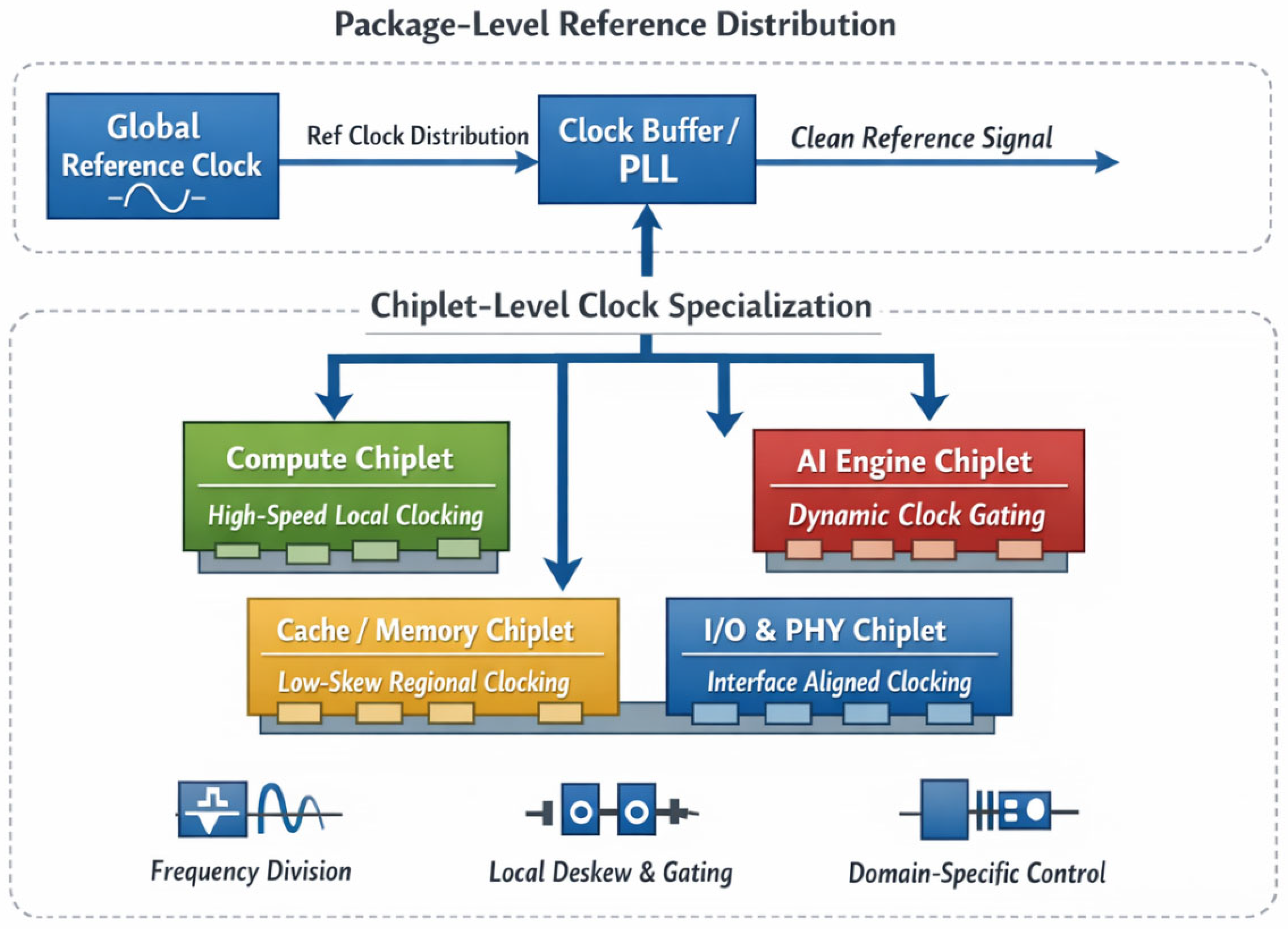
At the architectural level, communication has become a first-order design constraint. AI workloads are inherently multicast-heavy and data-movement intensive, placing significant pressure on on-chip interconnects. Traditional bus-based system-on-chip (SoC) designs struggle to scale, motivating the adoption of NoC architectures and hierarchical interconnect fabrics. Multicast-optimized and mesh-based NoCs, along with heterogeneous chip multiprocessor (CMP) chiplets, offer scalable solutions for high-throughput AI inference. In large heterogeneous chiplets, clock distribution and synchronization also become critical challenges. For example, energy-aware clock distribution strategies such as the Conical-Fishbone clock tree have been proposed to reduce skew and power consumption in multi-chiplet AI systems [15,16,17].
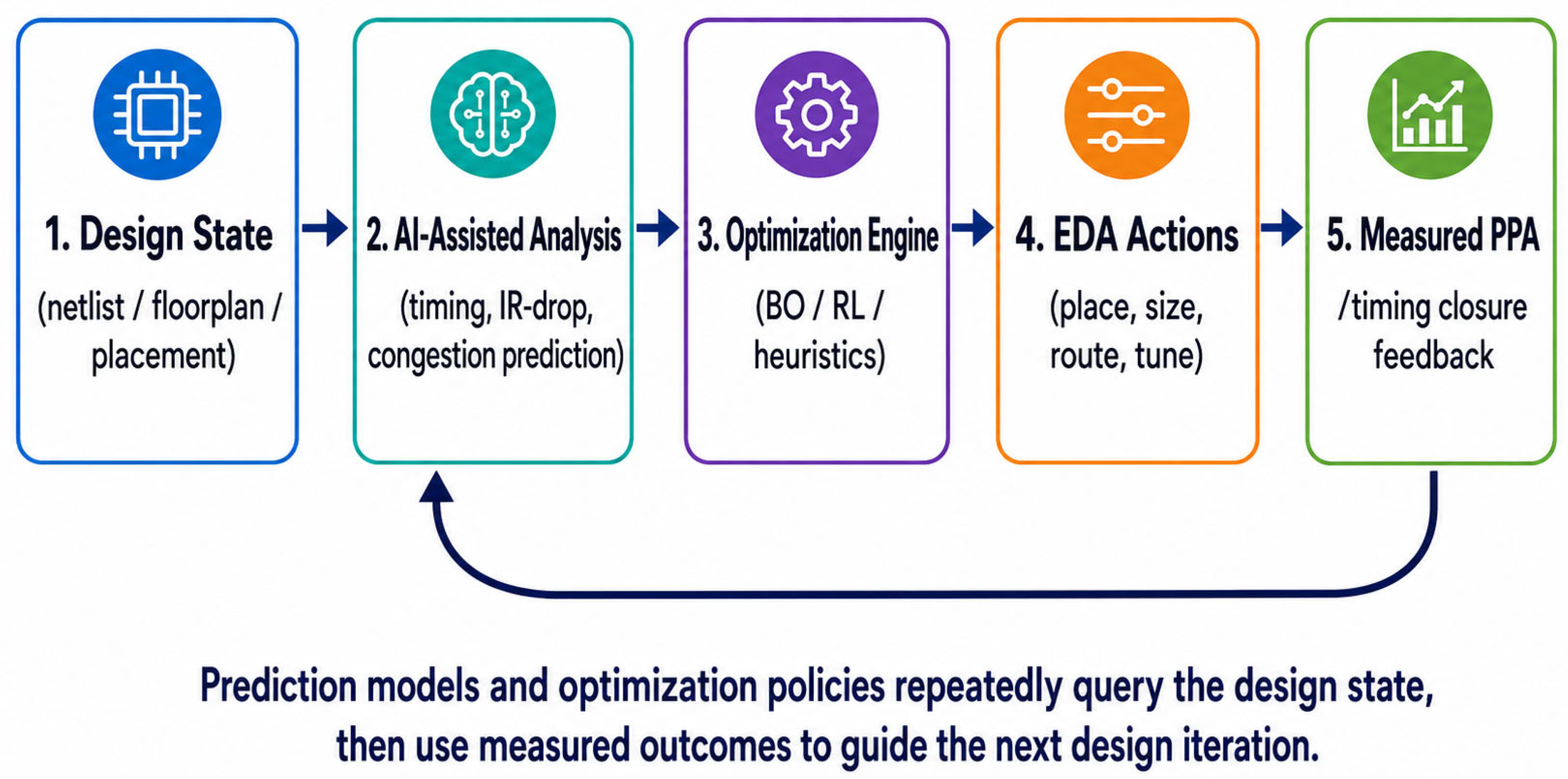
Simultaneously, AI is transforming the chip design process itself. Machine learning techniques are now employed for electronic design automation (EDA), including timing prediction, congestion analysis, and reinforcement-learning-based optimization. This “AI for chip design” paradigm complements “AI on chips,” forming a feedback loop in which AI accelerates hardware development while specialized hardware enables more advanced AI models [18,19,20].
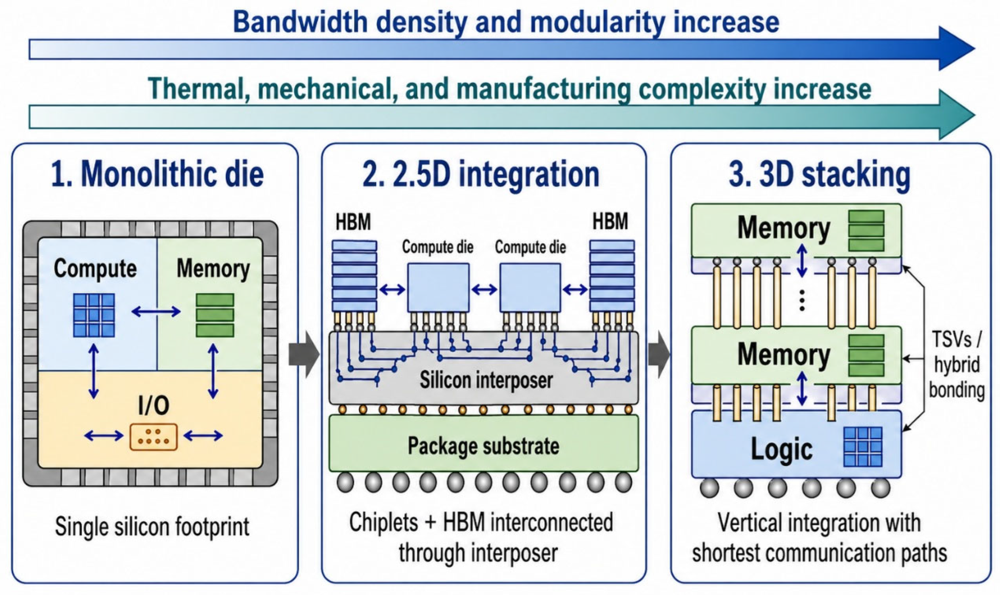
Manufacturing and packaging technologies further define the performance envelope of AI chips. High-density interconnects, 2.5D and three-dimensional (3D) integration, and advanced soldering techniques are essential to support chiplet communication, thermal management, and reliability. As AI chip complexity increases, yield optimization and long-term reliability become as important as peak computational throughput [21].
In parallel with silicon-based scaling, research in photonic computing, neuromorphic architectures, in-memory computing (IMC), and non–Von Neumann paradigms is redefining the boundaries of AI hardware. Photonic accelerators promise ultra-high bandwidth and energy-efficient matrix operations, while neuromorphic systems aim to emulate brain-inspired event-driven computation for sparse and adaptive processing. These approaches highlight a broader shift from pure digital acceleration toward heterogeneous, multimodal, and co-designed systems [7,22,23].
This review is organized to provide a comprehensive and structured perspective on AI-on-chip systems. Section 2 introduces a dual taxonomy of AI-on-chip paradigms, distinguishing functional roles (AI for design, AI on chips, and AI with chips) and structural forms (monolithic SoCs, NoC-enabled multi-core systems, and chiplet-based architectures). Section 3 surveys AI chip architectures across data-center GPUs, edge accelerators, FPGA-based systems, and heterogeneous chiplet platforms. Section 4 focuses on NoC architectures tailored for AI workloads, including multicast-aware interconnects and IIoT-enabled edge systems. Section 5 discusses model acceleration techniques and algorithm–hardware co-design methodologies. Section 6 addresses clocking, synchronization, and timing strategies in large-scale AI chips. Section 7 examines AI-driven design automation and the emerging role of large language models (LLMs) in EDA workflows. Section 8 reviews manufacturing, packaging, and reliability considerations. Section 9 explores emerging beyond-silicon paradigms, including photonic, neuromorphic, and in-memory AI hardware. Section 10 presents economic and industry perspectives, and Section 11 outlines open research challenges. Finally, Section 1 concludes with key insights and future outlooks for AI-on-chip systems.

2. Taxonomy of AI-on-Chip Paradigms

The rapid evolution of artificial intelligence (AI) workloads has fundamentally transformed semiconductor system design, leading to the emergence of specialized AI-on-chip paradigms optimized for performance, energy efficiency, scalability, and application adaptability. Unlike conventional computing architectures, AI chips integrate algorithmic intelligence directly into hardware through heterogeneous computing units, optimized dataflow mechanisms, and domain-specific accelerators. Recent developments span edge inference processors, lab-on-chip intelligent systems, heterogeneous programmable platforms, and large-scale GPU accelerators designed for high-performance computing environments.
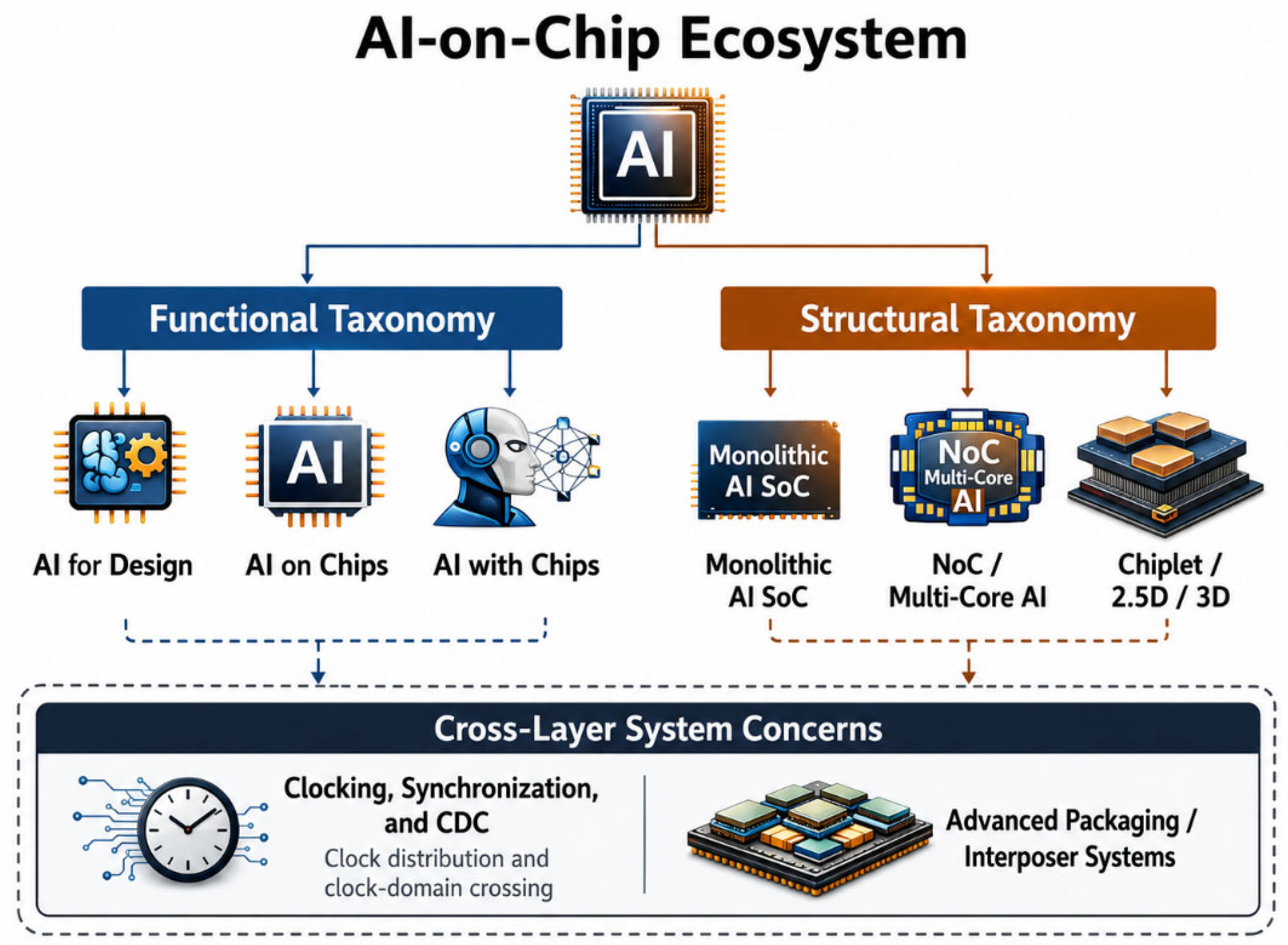
Based on functionality and architectural organization, AI-on-chip systems can be broadly categorized into functional taxonomy and structural taxonomy, as illustrated conceptually in Figure 1.

2.1. Functional Taxonomy

Functional taxonomy classifies AI-on-chip paradigms according to how artificial intelligence interacts with semiconductor design and system operation. Three dominant categories have emerged: AI for chip design, AI on chips, and AI with chips.

2.1.1. AI for Chip Design (EDA Automation and Optimization)

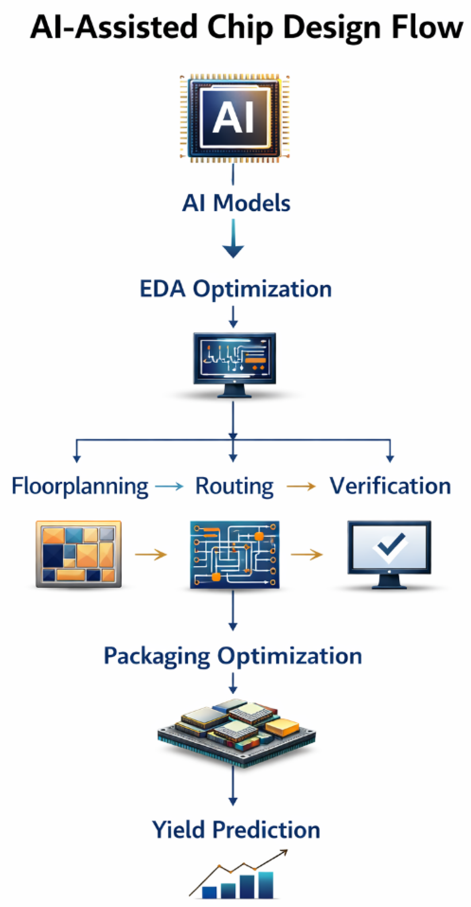
AI is increasingly playing a transformative role in semiconductor design and electronic design automation (EDA) workflows. The growing complexity of modern AI chips—often integrating hundreds of billions of transistors—demands intelligent optimization across multiple stages of development, including technology scaling, circuit layout, manufacturing yield, packaging reliability, and system-level performance as shown in Figure 2. Traditional design methodologies are increasingly insufficient to manage this multidimensional design space, motivating the integration of data-driven and learning-based optimization strategies [19,20,24].
Recent studies on graphics processing unit (GPU) co-optimization demonstrate that AI-driven methodologies can simultaneously optimize technology nodes, architectural configurations, algorithms, and deployment environments, enabling performance scaling beyond conventional Moore’s Law trends. These approaches incorporate design-for-manufacturing (DFM), reliability prediction, and intelligent testing mechanisms to jointly improve power efficiency, computational performance, and manufacturing yield. In parallel, architectural investigations highlight the growing importance of AI-assisted verification frameworks, including simulation-based fault injection and automated validation pipelines required for heterogeneous AI accelerators operating in mission-critical environments [25,26].
Within modern EDA ecosystems, AI-enabled tools are increasingly applied to several key design stages, including:
  • Floorplanning optimization
  • Routing congestion prediction
  • Thermal and power estimation
  • Manufacturing defect prediction
  • Yield optimization in advanced packaging technologies
Beyond circuit and layout optimization, manufacturing innovations further illustrate the impact of data-driven intelligence on semiconductor reliability. For example, optimized vacuum fluxless reflow processes and micro-bump interconnection analysis demonstrate how machine learning techniques improve packaging quality and yield in high-density AI chip integration.
These developments align closely with the emerging SysMoore paradigm, in which system-level co-optimization increasingly replaces transistor scaling as the primary driver of performance improvements. Under this paradigm, AI-assisted system-on-chip (SoC) optimization frameworks integrate machine learning with software-defined communication and networking concepts to enhance data exchange efficiency among densely integrated processing cores and heterogeneous computing elements. AI-driven design-space exploration enables substantial improvements in routing strategies, floor planning decisions, congestion mitigation, and power distribution analysis.
As conceptually illustrated in the SoC–network-on-chip (NoC) co-design framework discussed in this work, integrating AI with intelligent on-chip networking architectures significantly improves scalability for data-intensive workloads generated by emerging Internet of Things (IoT) and 5G/6G communication systems.
In addition, AI techniques are increasingly applied to critical verification and reliability tasks, including design rule check (DRC) prediction, layout optimization, yield enhancement, and packaging reliability assessment. Recent comprehensive reviews of advanced AI chip development further emphasize that next-generation optimization must simultaneously consider materials engineering, circuit design, architectural innovation, and advanced packaging technologies to achieve multimodal processing capability and improved energy efficiency.

2.1.2. AI on Chips (Inference, Perception, and Control)

The most widely recognized AI-on-chip paradigm embeds artificial intelligence computation directly into silicon to efficiently execute machine learning workloads. In this approach, neural network inference is performed within specialized hardware accelerators optimized for low latency and energy efficiency. These systems integrate neural network acceleration engines, specialized memory hierarchies, and optimized interconnect structures to support real-time processing at the edge, reducing reliance on cloud infrastructure.
Edge AI processors exemplify this category. Dedicated inference accelerators, such as the ARIES chip, achieve high computational throughput while maintaining low power consumption, making them suitable for embedded deployment environments. Its architecture integrates optimized deep learning acceleration engines and supporting software toolchains, enabling efficient deployment across multiple AI frameworks. Similarly, CNN-based embedded inference hardware implements convolutional neural networks directly within integrated circuits to minimize latency and energy consumption in vision applications, such as human detection systems. FPSoC (Field-Programmable System-on-Chip) is another platform that integrates microprocessors, memory (RAM), programmable logic blocks, and various input/output peripherals into a single configurable semiconductor device, enabling both software execution and hardware customization on the same chip. Table 1 shows examples of AI inference platforms and their applications.
Programmable heterogeneous platforms further extend this paradigm by integrating multiple compute resources within a unified system-on-chip (SoC) architecture, including:
  • CPU
  • Neural Processing Units (NPUs)
  • FPGA fabrics
  • Digital Signal Processors (DSPs)
This heterogeneous integration supports adaptable edge AI workloads and enables flexible acceleration strategies across diverse applications.
Key characteristics of AI-on-chip inference systems include:
  • Low-latency inference
  • Energy-efficient computation
  • Localized data processing
  • Reduced cloud dependence
Edge AI deployment increasingly relies on heterogeneous architectures combining CPUs, DSPs, neural processing engines, and dedicated inference accelerators. A representative example is the acceleration of YOLOv5 object detection models on embedded AI processors. Optimization strategies such as algorithm compression, convolution acceleration, and neural inference engine tuning significantly improve real-time performance under constrained power budgets [12].
The YOLOv5 AI-chip deployment architecture typically illustrates tight integration between [12,13]:
  • Neural Network Inference Engine (NNIE)
  • CPU/DSP subsystems
  • Image signal processors
  • Heterogeneous acceleration pipelines
These architectural optimizations enable practical edge applications, including:
  • Smart surveillance
  • Industrial monitoring
  • Autonomous inspection systems
Table 2 shows AI-on-Chip optimization techniques presented in [12,13].

2.1.3. AI with Chips (Co-Designed Intelligent Systems)

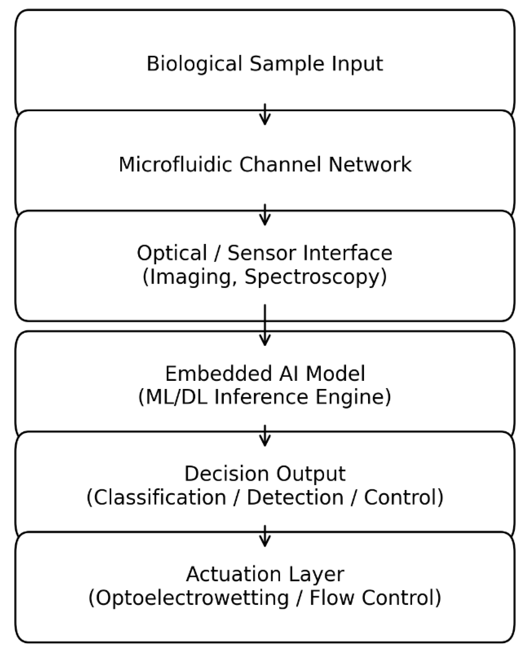
AI-with-chip paradigms integrate sensing, communication, and decision intelligence into unified cyber-physical platforms. Among the most prominent examples are AI-enabled lab-on-chip technologies, where sensing, computation, and control are co-designed within microscale environments as illustrated in Figure 3. For instance, AI-assisted optofluidic platforms analyze biological samples in real time using embedded machine learning models within microfluidic systems, enabling identification of cellular morphology or environmental characteristics without destructive testing. Similarly, AI-assisted optoelectrowetting chips leverage deep learning models to dynamically control droplet manipulation through adaptive light pattern generation, enabling programmable digital microfluidics without mechanical actuation.
These systems exemplify co-optimization across sensing, actuation, computation, and decision intelligence, producing unified intelligent platforms rather than loosely coupled subsystems. Their applications span biomedical diagnostics, environmental monitoring, smart laboratory automation, and autonomous chemical processing.
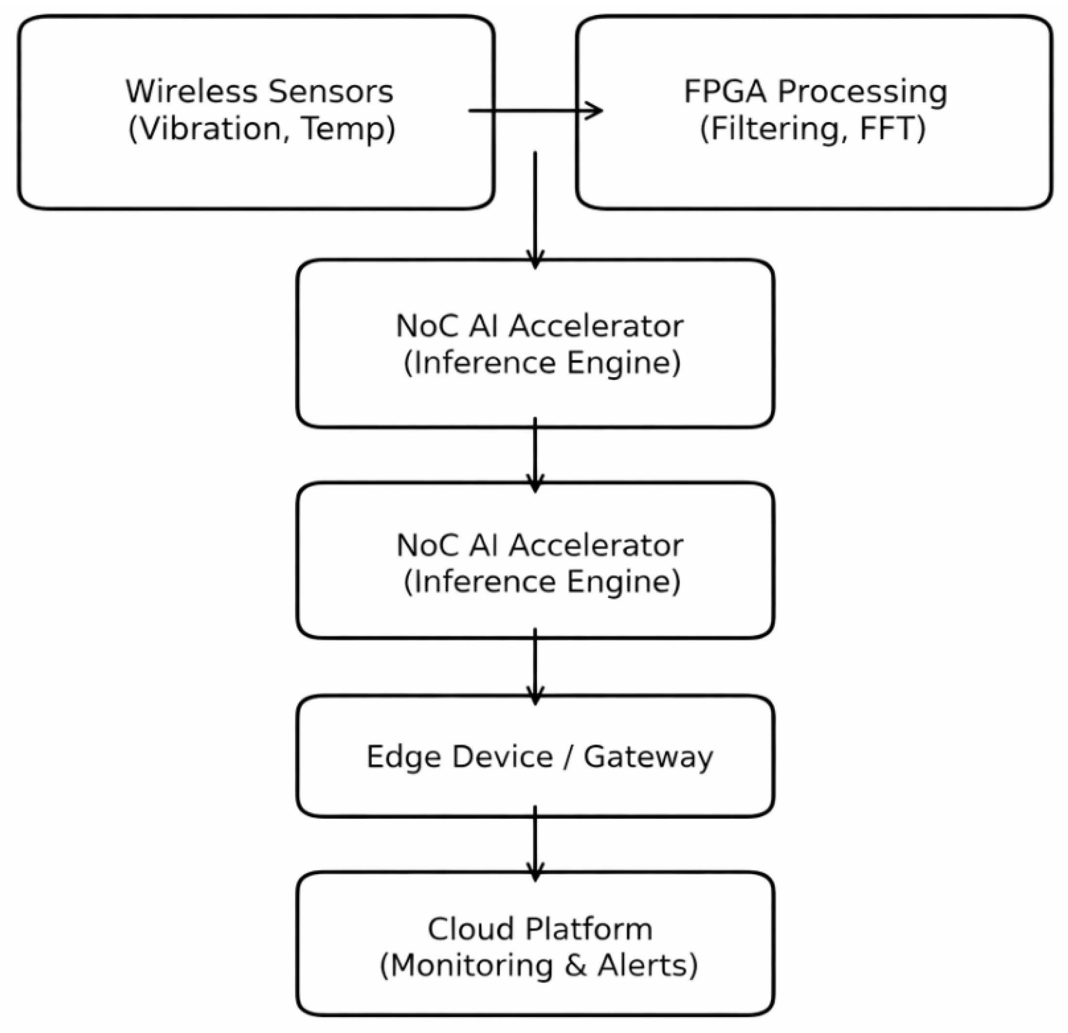
More broadly, AI-with-chip paradigms extend this integration beyond microscale bio-platforms to larger cyber-physical infrastructures, combining sensing, communication, and decision intelligence within cohesive architectures. A representative example is the Industrial Internet of Things (IIoT) fault diagnosis platform that integrates wireless sensors, FPGA-based preprocessing, and a Network-on-Chip (NoC) AI accelerator for real-time machinery monitoring [6]. In this architecture, vibration signals are captured by distributed wireless sensing modules, preprocessed on FPGA hardware, analyzed using NoC-based AI inference engines, and subsequently transmitted to cloud-connected edge devices for fault reporting and predictive analytics, as illustrated in Figure 4.
Such architectures enable predictive maintenance and intelligent monitoring in Industry 4.0 environments, demonstrating how tightly integrated sensing–communication–AI platforms are redefining real-time decision-making across biomedical and industrial domains. A comparison between Lab-on-Chip and IIoT AI-with-Chip systems is shown in Table 3.

2.2. Structural Taxonomy

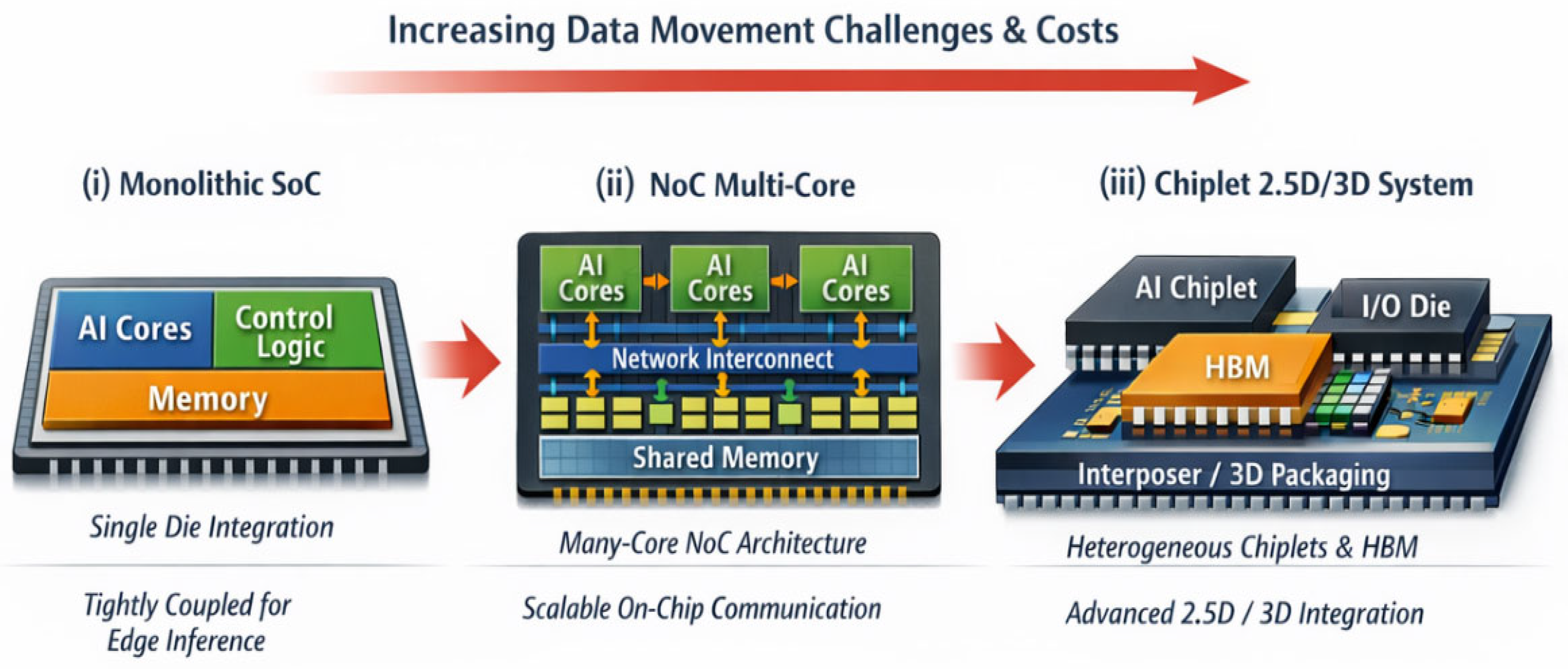
AI-chip architectures can be classified according to structural integration scale: (i) monolithic AI systems-on-chip (SoCs), (ii) network-on-chip (NoC)-enabled multi-core AI chips, and (iii) chiplet-based 2.5D/3D AI systems. Rather than treating these categories as unrelated product classes, the paper frames them as successive responses to the same underlying bottleneck: the rising cost of data movement relative to arithmetic as shown in Figure 5. Monolithic SoCs excel when control logic, accelerators, and memory interfaces must be tightly coupled on a single die, especially for edge inference. NoC-enabled many-core chips emerge when spatially distributed processing elements require explicit routing, multicast, and memory-hierarchy coordination. Chiplet and advanced-packaging approaches become attractive when reticle limits, yield pressure, heterogeneous process requirements, and HBM proximity dominate system design [17,27,28].

2.2.1. Monolithic AI SoCs

Monolithic AI SoCs place the main heterogeneous functions of an AI system within a single die. Typical blocks include host CPUs, neural-network accelerators, image-signal processors, codecs, security logic, memory controllers, and peripheral I/O. Their central strength is tight integration: the designer can coordinate task scheduling, data formatting, sensor ingress, and accelerator execution without crossing a package boundary. This makes monolithic SoCs especially well suited to edge devices, embedded vision, robotics, automotive subsystems, and battery-constrained systems where latency, integration cost, and power matter as much as peak arithmetic throughput.
There are several examples of this logic. Mobilint’s ARIES is presented as an edge-AI inference chip manufactured in a 14 nm process with 64 TOPS peak performance (80 TOPS boost) and tightly integrated on-chip memory and control logic. The CNN-based human-head-detection and the fully programmable heterogeneous FPSoC similarly reflect the monolithic or tightly integrated edge-AI design philosophy, where inference, control, and peripheral functions are placed as close as possible to reduce latency and board-level overhead [29,30].
Architecturally, monolithic SoCs benefit from short on-die interconnects, unified clocking strategies, and simplified coherency domains. They can also exploit local SRAM aggressively. Canonical single-die AI accelerators such as TPU-class systolic processors and Eyeriss illustrate how strong locality and dataflow-aware memory reuse can produce large efficiency gains when the working set can be staged near compute [31,32,33].

2.2.2. NoC-Enabled Multi-Core AI Chips

NoC-enabled AI chips arise when distributed compute must be treated as a first-class architectural problem. In these chips, accelerators are not just large blocks attached to a host fabric; they are arrays or clusters of processing elements whose efficiency depends on systematic data distribution, multicast, reduction, and buffer reuse. The NoC is therefore not merely an implementation detail. It is often the central enabler of scalability.
The mTREE paper is directly relevant here. It shows that AI-chip traffic is heavily multicast-oriented because neural-network data are repeatedly broadcast from shared buffers to many compute endpoints. By modifying router microarchitecture for multicast, the work shows how the NoC structure itself can become a first-order optimization variable rather than just a background transport mechanism [34].
NoC thinking, where a NoC AI chip is combined with wireless sensing and FPGA-based preprocessing to support real-time multi-machine diagnosis and notification, is also analyzed in the literature. Although it is system-level rather than purely architectural, it reinforces the point that communication organization is central once computation is spatially distributed [4,6].
The tradeoff is that NoC-centered chips move complexity from packaging to microarchitecture and mapping. Congestion, arbitration, deadlock avoidance, credit management, synchronization, memory tiling, and placement all become decisive. Performance is often strongly workload-dependent: a network optimized for regular tensor broadcast may be much less effective for irregular sparsity or control-heavy inference. Nevertheless, once a design reaches many-core scale, a structured NoC is usually more principled than an oversized shared bus. This is why NoC designs remain a defining middle layer in the taxonomy between single-die SoCs and package-level chiplet systems.

2.2.3. Chiplet-Based 2.5D/3D AI Systems

Chiplet-based AI systems separate the design into multiple dies while using advanced packaging to preserve enough bandwidth that the overall system behaves like a tightly integrated accelerator. In 2.5D integration, chiplets communicate through an interposer or other high-density package substrate; in 3D integration, vertical stacking and through-silicon vias move memory or logic into closer proximity. In this class, packaging becomes part of architecture rather than only a manufacturing afterthought [17,35].
The uploaded literature already points in this direction. The nano-Abacus chiplet paper describes a 2.5D SoC integrating a silicon interposer, a 3D memory stack, an FPGA, and three computational chiplets, while the conical-fishbone clock-tree work highlights one of the less-discussed but important chiplet problems: scalable clock distribution in heterogeneous multi-die systems [17,36].
Recent industrial accelerators reinforce this trend. AMD’s MI300X uses a multi-chip package and high-bandwidth memory to combine large local capacity with dense accelerator communication. Intel’s Ponte Vecchio and NVIDIA’s recent multi-die GPU packages similarly show that advanced packaging is now the scaling vehicle for high-end AI systems, while wafer-scale engines push the idea further by expanding the compute domain itself [37,38,39,40,41].
Chiplet systems offer three major architectural benefits. First, they allow function-specific partitioning: compute, I/O, SRAM/cache, analog PHYs, and memory interfaces need not share the same optimal process technology. Second, they improve manufacturability and binning flexibility relative to a single extremely large monolithic die. Third, they shorten the effective distance to HBM or other high-capacity memory resources, which is increasingly critical for transformer-class workloads. Their challenges are equally important: package design, thermal management, die-to-die coherency, test coverage, known-good-die strategy, and software/runtime awareness. As packaging becomes an architectural resource, validation and system orchestration become harder, not easier.

2.2.4. Directions of Structural Taxonomy

The three classes should not be interpreted as winners and losers. They are better understood as structurally different responses to specific system objectives. Monolithic SoCs are generally preferred when sensor integration, deterministic latency, low board cost, or tight power envelopes dominate. NoC-enabled multi-core chips are compelling when the primary challenge is on-chip scaling of dataflow-rich computation across many processing elements. Chiplet-based and 2.5D/3D systems become attractive when the arithmetic engine, memory system, and product scale exceed what is practical on one die. Table 4 compares the three structural classes.
A second observation is that modern AI hardware often combines the classes. A chiplet package may contain monolithic accelerator chiplets, and each chiplet may internally rely on a NoC. Thus, the taxonomy is layered rather than exclusive. The most advanced systems increasingly operate at all three levels at once: local monolithic integration inside each die, structured NoC communication inside the die, and package-level fabrics between chiplets and HBM stacks.
A third observation concerns software. The further one moves from monolithic SoCs toward chiplet systems, the more architectural value depends on mapping and runtime quality. Compiler partitioning, graph lowering, tensor tiling, collective communication scheduling, memory placement, and fault handling increasingly determine realized efficiency. This is one reason industrial white papers emphasize co-optimization across technology, architecture, system, and algorithm rather than treating the chip as a self-contained artifact.
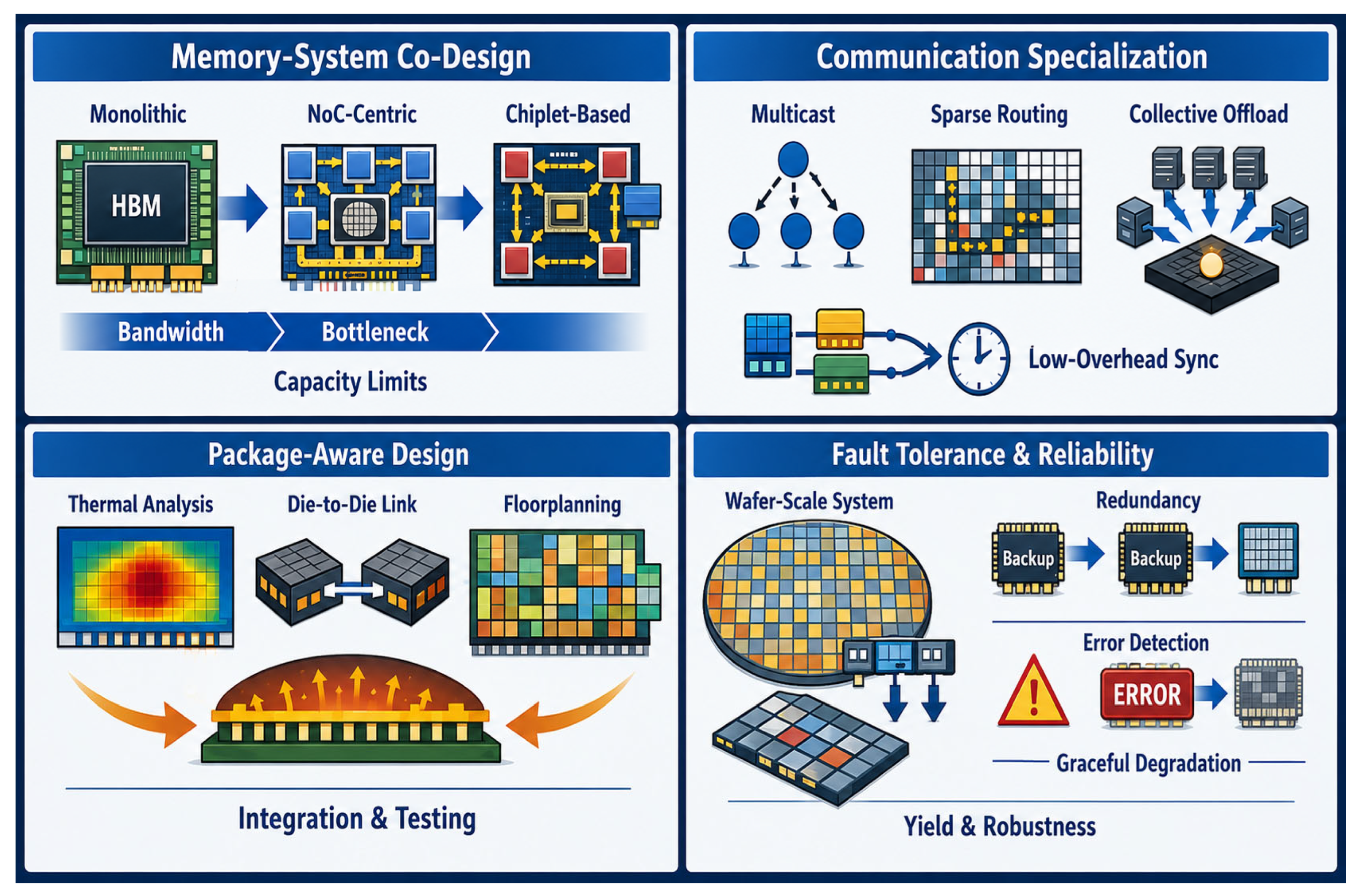
Several research questions cut across the taxonomy. First, memory-system co-design remains central. Whether the platform is monolithic, NoC-centric, or chiplet-based, bandwidth and capacity limits dominate utilization on modern AI workloads. Second, communication specialization is increasingly valuable. Multicast support, sparsity-aware routing, collective offload, and low-overhead synchronization are becoming architectural differentiators. Third, packaging-aware design methodologies remain immature relative to classic single-die flows. Thermal analysis, package-aware floorplanning, die-to-die protocol verification, and test strategy need tighter integration with AI workload models.
A related direction is fault tolerance and graceful degradation. This is visible both in industrial-scale packages and in wafer-scale systems, where yield and reliability must be handled architecturally rather than hidden below the software stack. Figure 6 summarizes these research challenges [38,42].

3. AI Chip Architectures and Hardware Platforms

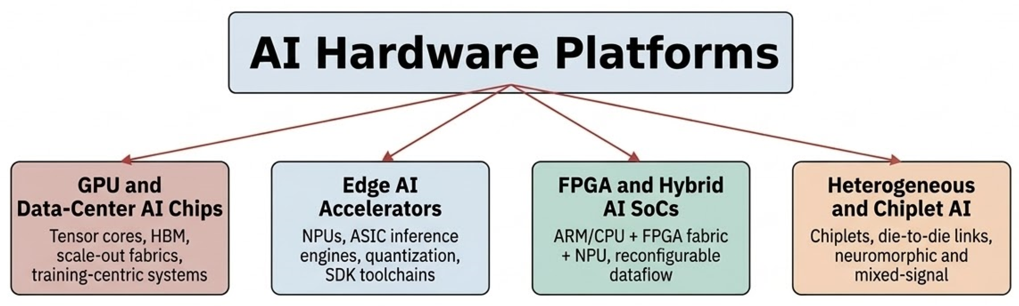
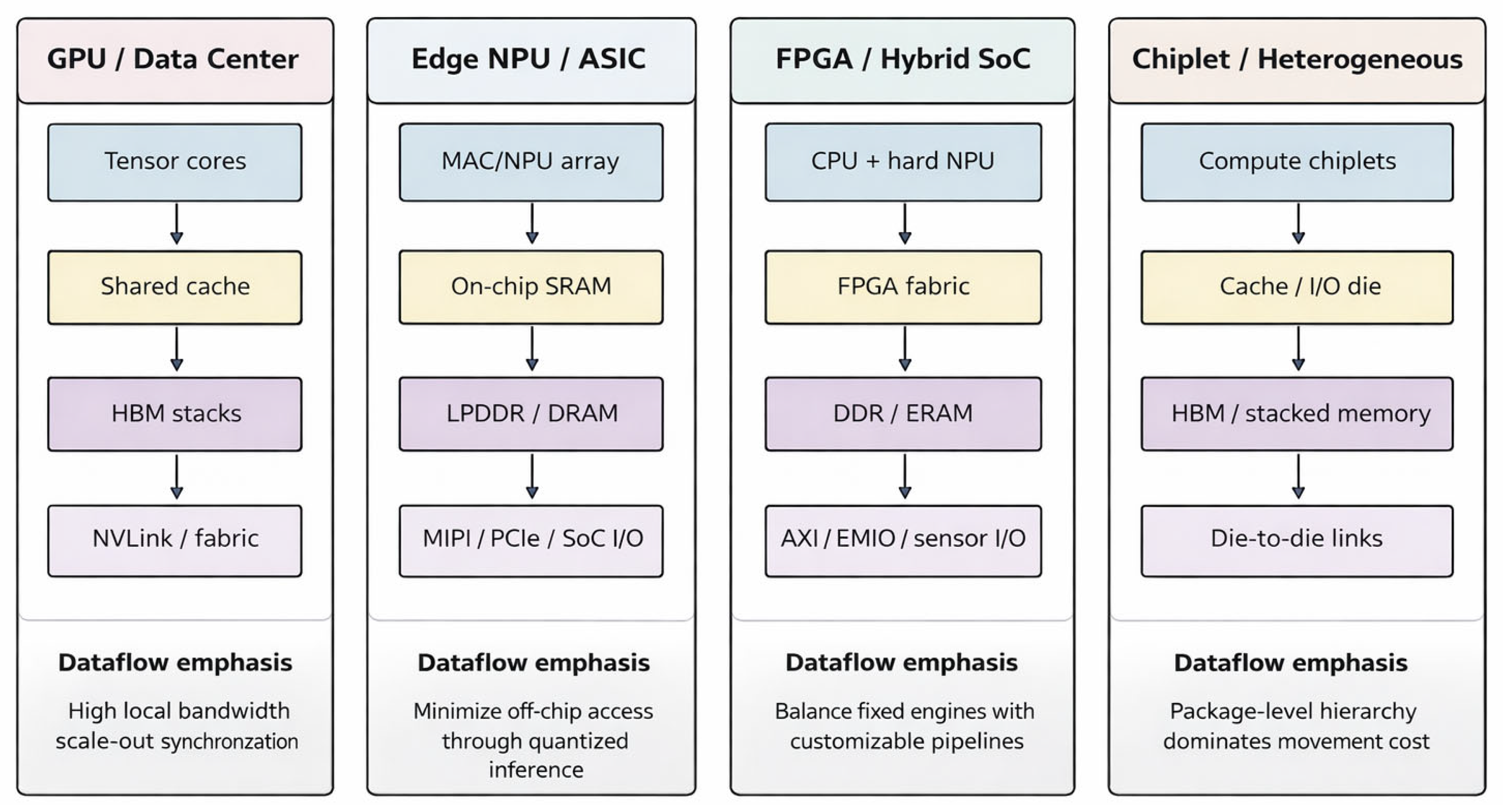
The rapid growth of deep learning workloads has driven a clear diversification of hardware platforms for artificial intelligence. Instead of relying on a single dominant architecture, the field now spans training-oriented GPUs and data-center accelerators, low-power edge NPUs and ASICs, FPGA-based and hybrid SoCs, and increasingly heterogeneous chiplet-based systems as summarized in Figure 7. This diversification is largely a response to the mismatch between AI workload characteristics and conventional von Neumann computing, especially under the pressure of memory bandwidth, interconnect efficiency, latency, power density, and deployment flexibility. Recent reviews and application papers consistently show that AI-chip design has become a multi-objective optimization problem involving compute throughput, data movement cost, programmability, packaging, and software–hardware co-design [36].

3.1. GPU and Data-Center AI Chips

3.1.1. Training-Centric Architectures

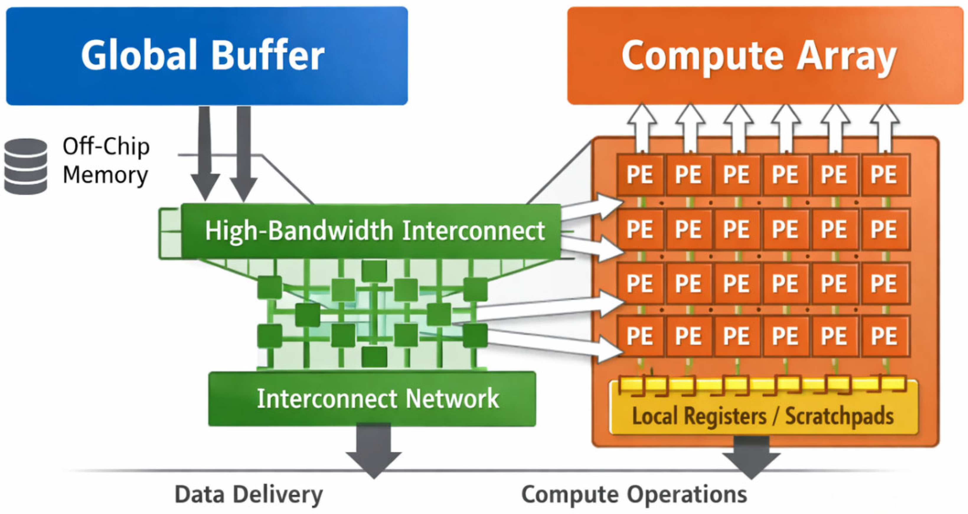
GPUs remain the dominant platform for large-scale AI training because their massive parallel execution model maps effectively onto dense linear algebra, tensor operations, and mixed-precision training. Modern data-center GPUs are no longer merely graphics processors adapted for machine learning; they are now highly specialized training-centric architectures built around tensor cores, high-bandwidth memory, and large-scale interconnect fabrics. For example, NVIDIA’s Hopper-based H100 integrates tensor-oriented acceleration units, support for the Transformer Engine, and HBM3 memory to target large language models and other compute-intensive AI workloads. As illustrated in Figure 8, these systems rely on a hierarchical organization in which high-throughput compute units are tightly coupled to high-bandwidth local memory, while multi-GPU scaling depends on dedicated communication fabrics [43].
In this context, NVLink serves as a high-bandwidth direct GPU-to-GPU interconnect, whereas NVSwitch acts as the switching fabric that connects multiple GPUs and enables all-to-all communication at NVLink speed within a server or scale-up domain. This communication layer is critical for large-model training because it reduces bottlenecks associated with model parallelism, tensor exchange, and collective communication [44,45]. At hyperscale, AI training is not governed solely by chip-level performance, but by the architectural design of the full supercomputing system. Google’s TPU v4 demonstrates this system-level orientation by combining domain-specific matrix acceleration with optically reconfigurable interconnect support, showing that large-scale training increasingly depends on topology-aware communication and system-level co-design [46]. Likewise, recent architectural reviews emphasize that state-of-the-art AI training systems have shifted from CPU-centric nodes toward heterogeneous accelerator-centric clusters that combine GPUs, high-bandwidth memory, and high-speed communication fabrics [7].
A common architectural pattern in training-oriented platforms is therefore the co-optimization of matrix engines, local memory bandwidth, inter-accelerator communication, and compiler/runtime support. This is particularly critical for transformer-based workloads, in which arithmetic throughput alone is insufficient; performance is increasingly limited by the cost of moving activations, weights, and optimizer states across memory hierarchies.

3.1.2. Energy and Scalability Challenges

Despite their performance advantages, GPU-centric AI platforms face persistent energy and scalability limitations. A major challenge is that data movement often consumes more energy than arithmetic itself. Even with tensor-core acceleration, the training of frontier AI models is constrained by memory bandwidth, synchronization overhead, collective communication costs, and rack-level power and thermal limits. As model and cluster sizes continue to grow, scaling efficiency tends to degrade because the cost of all-reduce operations, parameter synchronization, and remote memory access increases significantly [7,47].
These challenges are pushing the field toward more communication-aware and memory-rich architectures. AMD’s MI300 family, for instance, illustrates this trend by emphasizing large HBM capacity and very high local memory bandwidth to reduce off-package traffic and improve support for large-model execution [40]. More broadly, recent literature identifies packaging, memory-system design, thermal density, and interconnect scalability as primary constraints in next-generation AI accelerators. Consequently, the central bottleneck in data-center AI hardware is no longer compute alone; it is the scalable and energy-efficient movement of data across memory, package, board, and cluster boundaries [7].

3.2. Edge AI Accelerators

3.2.1. NPUs and ASIC Accelerators

Edge AI accelerators have emerged as a distinct hardware class because the optimization goals of edge inference differ fundamentally from those of cloud and data-center AI. Rather than maximizing absolute training throughput, edge platforms are typically designed around low latency, low power, compact form factor, thermal limits, and deployment cost, while still maintaining enough compute density for real-time inference in vision, audio, robotics, and industrial systems [7,29,30,48,49]. In this context, NPUs (neural processing units) and edge-oriented ASIC accelerators are especially important because they provide dedicated support for neural-network inference with much better performance-per-watt than general-purpose CPUs and, in many scenarios, better deployment efficiency than discrete GPUs [7].
A representative example from the uploaded literature in [48], explicitly presented as an edge AI chip rather than a general-purpose processor. It describes ARIES as a dedicated edge AI accelerator and highlights its emphasis on deployment-oriented metrics such as inference performance, system integration, and software support rather than training capability alone [48]. A later production announcement about the same platform reports that ARIES was commercialized as a 14 nm AI inference SoC tested across more than 200 open-source deep-learning models and targeted at applications such as robotics, smart-city infrastructure, healthcare diagnostics, edge servers, and cloud-edge inference. Together, these sources illustrate an important point: modern edge AI accelerators are increasingly designed as application-directed inference platforms that combine model execution efficiency with a deployment-ready software stack [48,50].
In [30], this same architectural direction, from the application side, is reinforced. That work describes an integrated human-head detection pipeline implemented on an edge AI chip and shows how a dedicated CNN-capable hardware platform can support practical embedded vision tasks in indoor detection scenarios. The significance of this kind of system is not merely that inference occurs on-device, but that the hardware is tailored to the restricted model family, latency target, and energy envelope of the target application. In edge deployments, this specialization can be more valuable than raw peak throughput because real-world systems are constrained by board power, heat dissipation, sensor interfaces, and standalone operation [30].
From an architectural standpoint, NPUs and edge ASICs commonly rely on a few recurring design strategies: low-precision arithmetic, operator fusion, static dataflow scheduling, aggressive on-chip buffering, and limited but efficient support for dominant neural-network kernels such as convolution, matrix multiplication, depthwise convolution, and activation operations. This approach contrasts with data-center GPUs, which prioritize broader programmability and higher training throughput. In edge devices, the dominant objective is usually to reduce external memory traffic and maximize useful inference work per joule. For this reason, many edge accelerators emphasize local SRAM usage, quantized execution, and streamlined execution paths that avoid the software and energy overhead of more general-purpose architectures [29,30,48,49].
The FPSoC design presented in [32] is also relevant here, as it shows that edge AI systems often combine NPU-style fixed-function acceleration with configurable logic and embedded processors rather than relying solely on a fixed datapath. That paper presents a fully programmable heterogeneous FPSoC integrating processors, NPU resources, JPEG processing, and FPGA logic to improve both acceleration capability and flexibility for edge AI applications. Although this platform falls into the hybrid SoC category, it remains highly relevant to edge AI because it demonstrates that practical edge deployments often require a mix of dedicated inference acceleration and configurable system-level support rather than a single monolithic compute block [29].
Overall, the literature suggests that edge NPUs and ASIC accelerators should be viewed less as “small GPUs” and more as specialized inference engines embedded within a larger system context. Their architectural value lies in their focus on the hardware requirements of deployment: compact models, quantized execution, real-time response, modest cooling, and direct interaction with sensors or embedded control logic.

3.2.2. SDK-Driven Deployment Ecosystems

A second defining feature of edge AI is that hardware competitiveness depends not only on silicon capability but also on the quality of the deployment ecosystem surrounding the device. In practice, an edge accelerator is useful only if trained models can be converted, quantized, compiled, profiled, deployed, and maintained through a stable software workflow. For this reason, many successful edge AI platforms are best understood as SDK-centered systems where the SDK (software development kit) provides the software tools, libraries, compilers, and runtime interfaces needed to convert trained models into deployable applications [29,48,49].
This point is especially clear in [48], which describes the company’s qb SDK as a central component of the platform. It states that the SDK supports deployment from major frameworks, including ONNX, TensorFlow, PyTorch, and TVM, and provides compilation and runtime support through software interfaces such as Python and C++ APIs. This type of stack is critical because it bridges the gap between model training and field deployment. Without such an SDK, even a high-performance edge chip would be difficult to integrate into production workflows. Thus, in edge AI, the software layer is not secondary to the hardware; it is part of the accelerator architecture itself [48].
In [29], the argument is made from a different angle. It describes a deployment flow in which models are trained offline, quantized, and converted, then mapped across heterogeneous hardware resources, including CPU cores, hard NPU blocks, soft NPU logic, and FPGA fabric. This workflow shows that edge inference increasingly depends on compiler–runtime–hardware co-design, especially when different parts of a model or application pipeline must be assigned to different compute resources. In such systems, the deployment framework determines whether the underlying hardware can actually be used efficiently in practice.
This SDK-centered pattern is also visible in widely used commercial edge ecosystems. Google’s Edge TPU software model requires neural networks to be converted to TensorFlow Lite and then compiled specifically for the Edge TPU, with the compiled model executed on Coral devices [49,51,52]. Coral’s official documentation explicitly presents the Edge TPU as part of a deployment workflow that includes model compatibility checking, compilation, APIs, and supported runtimes rather than as a standalone chip. In other words, successful edge deployment depends not only on having an accelerator on the board, but also on a practical path from the trained model to the executable artifact [49,51,52].
A similar principle applies to GPU-based inference deployment with NVIDIA TensorRT, which NVIDIA describes as a high-performance inference SDK that imports trained models, applies graph optimization and layer fusion, and generates an optimized runtime engine with C++ and Python APIs. Although TensorRT is often used in larger embedded GPU devices rather than minimal NPUs, it illustrates the same broader lesson: edge and embedded AI performance is increasingly determined by the maturity of the deployment stack, including optimization tools, parsers, runtimes, precision support, and developer tooling [53].
Therefore, edge AI accelerators should be analyzed as full-stack platforms whose value depends on the interaction among hardware datapaths, memory systems, compilers, quantization flows, and runtime APIs. This is one of the clearest distinctions between edge AI and traditional embedded processing. In edge AI, the deployment SDK is not merely a convenience layer; it is a core architectural enabler that determines portability, ease of integration, optimization quality, and ultimately the real-world usability of the hardware [29,48,53].
Representative edge AI platforms and their deployment characteristics are summarized in Table 5, which compares the hardware class, architectural emphasis, software ecosystem, and practical deployment implications of selected edge AI accelerators.

3.3. FPGA and Hybrid AI SoCs

3.3.1. ARM-FPGA-AI Integration

FPGAs and hybrid AI SoCs occupy an important middle ground between fixed-function ASICs and fully programmable processor platforms. Their value lies in integrating heterogeneous elements—typically ARM processors, programmable logic, dedicated AI engines, memory controllers, and peripheral interfaces—into a single platform. This integration enables embedded AI systems to perform control, signal processing, data pre-processing and post-processing, and neural-network inference on the same device [6,29]. In practice, this architecture reduces board complexity and avoids the latency and power penalties associated with partitioning these functions across multiple chips.
The fully programmable heterogeneous FPSoC is especially relevant in this regard in [29]. Its architecture integrates CPU cores, hard NPU, soft NPU, FPGA fabric, and media acceleration in a single device, arguing that earlier split-chip SoC-plus-FPGA solutions suffered from inter-chip communication overhead, board complexity, and additional power loss [29]. By moving these functions onto a single heterogeneous platform, the design reduces latency and improves bandwidth efficiency. This type of organization is representative of a broader ARM–FPGA–AI integration trend, in which scalar processors manage system control and software execution, hardened AI blocks accelerate common neural-network kernels, and programmable logic implements custom data paths or application-specific interfaces [29].
This integration pattern is especially useful in industrial and embedded systems where sensor interfaces, safety logic, protocol handling, and evolving AI pipelines must coexist. The uploaded industrial IoT fault-diagnosis system similarly demonstrates a practical architecture that combines sensing, preprocessing, and AI inference across a heterogeneous hardware stack [6]. More broadly, adaptive computing platforms such as AMD Versal illustrate how programmable logic, scalar processing systems, and AI Engines can be combined in one heterogeneous device to support both deterministic system integration and AI acceleration [54]. AMD’s official architecture documentation likewise describes Versal adaptive SoCs as platforms that combine programmable logic, processing systems, AI Engines, and memory/interfacing resources for heterogeneous acceleration across edge and embedded workloads.

3.3.2. Reconfigurability Versus Performance

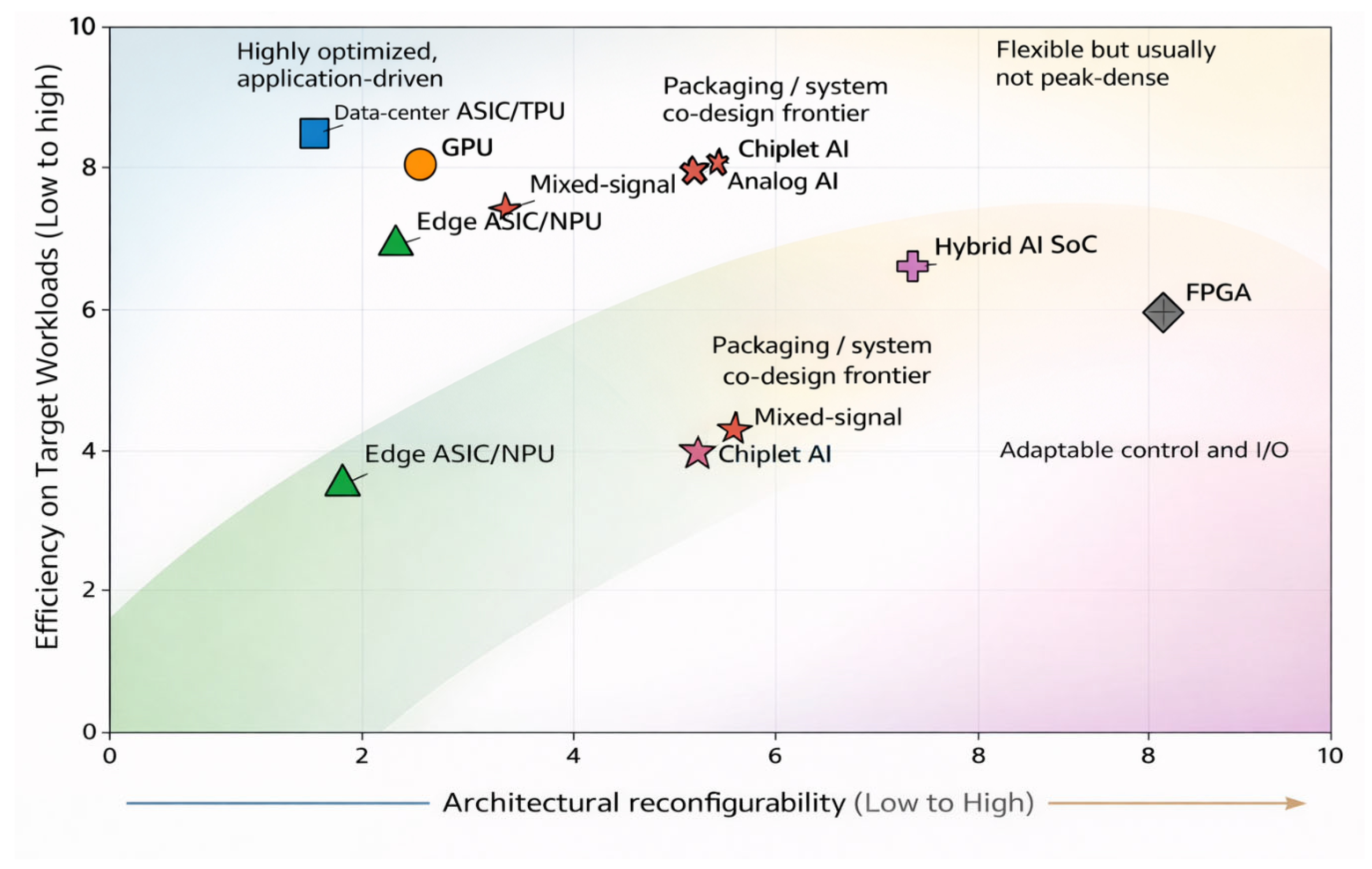
The classical tradeoff in FPGA-based AI systems is between reconfigurability and peak performance efficiency, and this tradeoff is the central idea conveyed in Figure 9. In the figure, the horizontal axis represents reconfigurability, meaning the extent to which a platform can be adapted to new models, operators, dataflow patterns, interfaces, or application requirements without redesigning the silicon. The vertical axis represents performance/efficiency, i.e., the platform’s practical ability to deliver high throughput and favorable energy or area efficiency for AI workloads. Under this interpretation, platforms positioned toward the upper-left of the figure emphasize high fixed efficiency with less flexibility, whereas platforms toward the lower-right emphasize adaptability at the cost of lower peak specialization.
As shown in Figure 9, ASIC accelerators are placed near the high-performance but low-reconfigurability region because they are hardened for specific data paths and neural-network operations. This specialization enables excellent throughput, energy efficiency, and area efficiency, but it also makes ASICs less adaptable when workloads, operators, or deployment requirements change. Prior comparative work on FPGA-versus-ASIC acceleration similarly notes that FPGA reconfigurability is attractive precisely because deep-learning models evolve rapidly, while ASICs generally retain an advantage in raw performance and area efficiency for fixed workloads [29].
By contrast, FPGAs are placed farther toward the reconfigurable side of Figure 9 because the programmable logic fabric can be re-synthesized to support new operators, custom bit widths, modified pipelines, or application-specific interfaces. This flexibility makes FPGAs highly attractive in environments where workloads evolve or where inference must be tightly integrated with unconventional I/O and pre/post-processing stages. However, Figure 9 also places FPGAs below ASICs in performance/efficiency because fine-grained programmability incurs overhead in logic utilization, routing, clock frequency, and tool complexity. Recent surveys of FPGA-based AI acceleration similarly position FPGAs as a middle-ground solution that offers substantially more flexibility than ASICs, but usually lower peak efficiency than a hardened accelerator designed for the same stable workload [29].
Hybrid SoCs appear in Figure 9 between pure FPGAs and fixed ASIC accelerators because they attempt to balance both objectives. Their placement reflects the fact that they combine hardened components—such as ARM cores, NPUs, DSP blocks, or AI Engines—with programmable fabric. In other words, the hard blocks provide efficient execution for common operations, while the programmable logic preserves adaptability for custom operators, protocol handling, sensor fusion, or pre/post-processing. The heterogeneous FPSoC in [29] makes this compromise explicit: its hard-NPU-plus-soft-NPU architecture uses hardened resources for common neural-network kernels while retaining programmable logic to extend the design when models or operator requirements change. AMD Versal devices illustrate this same principle at the commercial-platform level, combining processing systems, programmable logic, and AI Engines in a single architecture for heterogeneous acceleration [29].
The broader comparison in Figure 9 can also be interpreted relative to the other platform classes shown. CPUs appear as highly programmable but relatively low in AI-specific performance efficiency because they offer general-purpose programmability rather than specialized matrix acceleration. GPUs occupy a higher-performance position than CPUs because of their massively parallel tensor-oriented execution model, but they remain less reconfigurable than FPGA-style fabrics because their architecture is still largely fixed at the hardware level. Chiplet-based systems are placed high in performance because they can scale compute, memory bandwidth, and package-level integration, but their reconfigurability is only moderate: chiplets improve modularity and design reuse more than they provide post-fabrication programmability. Finally, neuromorphic platforms are shown as highly specialized alternatives whose value lies in sparse, event-driven, or ultra-low-power operation rather than conventional dense throughput; accordingly, they may provide very favorable efficiency in niche workloads but do not currently offer the broad programmability or software maturity of CPUs, GPUs, or FPGA-based systems. Reviews of neuromorphic computing similarly describe these systems as promising for efficient event-driven computation, but still limited by tooling, application generality, and ecosystem maturity.
FPGA and hybrid SoC platforms remain attractive when model evolution is expected, pre-/post-processing is substantial, I/O integration matters, or application-specific dataflow must be supported. In contrast, when the workload is stable and dominated by mainstream dense operators, dedicated ASICs and NPUs usually provide better energy efficiency and higher peak performance. This is precisely why FPGA- and hybrid-AI SoCs continue to play an important role in embedded, industrial, robotics, and edge deployments, where system-level flexibility is often as important as neural network throughput [6,29].

3.4. Heterogeneous and Chiplet-Based AI Architectures

3.4.1. Chiplet Communication and Memory Hierarchies

As AI models continue to increase in parameter count, activation size, and communication intensity, monolithic chip scaling is increasingly constrained by reticle limits, yield degradation, power density, and memory bandwidth. These pressures have accelerated the transition toward heterogeneous, chiplet-based AI architectures, in which compute, memory, I/O, and control functions are partitioned across multiple dies and integrated into a common package. Rather than treating packaging as a downstream implementation detail, recent AI-chip research treats package topology, die partitioning, and memory placement as first-order architectural variables because they directly affect bandwidth, latency, thermal behavior, and scalability [7,55].
In such systems, the central design problem is the organization of communication and memory hierarchies. A chiplet-based AI processor typically separates compute chiplets from memory resources such as HBM stacks, cache dies, or I/O dies, and relies on short-reach die-to-die links to sustain data movement within the package. The efficiency of this arrangement depends on how well the architecture minimizes off-package traffic while preserving sufficient bandwidth among distributed compute elements. The UCIe consortium has formalized this direction by defining an open die-to-die interconnect framework intended to support interoperable chiplet ecosystems and to address practical issues such as testability, manageability, and debug across the chiplet lifecycle [55]. In this context, die-to-die interconnects refer to physical and protocol-level links that connect chiplets inside the same package, while HBM (high-bandwidth memory) denotes stacked near-package memory designed to provide much higher bandwidth than conventional external DRAM [7,55].
For AI workloads, chipletization is attractive because it enables modular scaling of compute and memory without requiring an increasingly large monolithic die. However, the benefits depend strongly on the communication substrate. AI training and inference involve frequent multicast, reduction, and many-to-many data exchange patterns, so the package-level interconnect must support much more than simple point-to-point traffic. This is consistent with the uploaded mTREE work, which shows that AI-oriented NoC design can benefit from customized multicast support rather than relying on generic communication topologies. That paper argues that multicast-aware NoC structures reduce communication overhead and energy relative to less specialized alternatives, which is directly relevant to future chiplet AI systems in which distributed data reuse and collective movement become dominant bottlenecks. The architectural implication is that chiplet-based AI systems should be analyzed not only as collections of dies, but as coordinated memory-and-communication fabrics whose performance is limited by inter-chiplet data motion as much as by local arithmetic throughput [34].
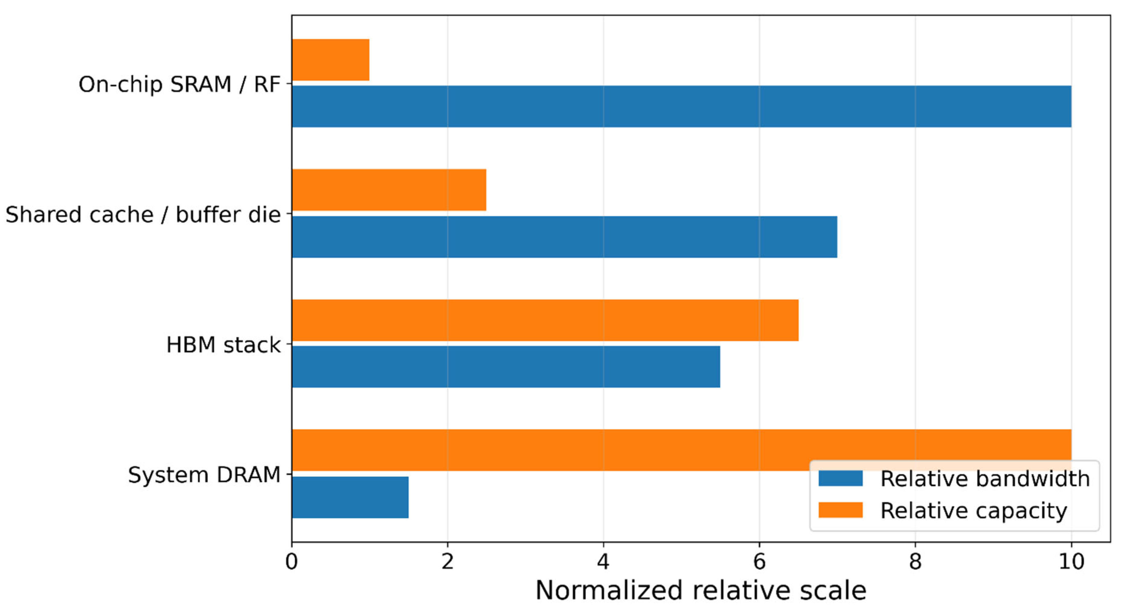
This architectural shift is also reflected in the memory hierarchy itself. In a chiplet-based AI platform, memory is best understood as a layered hierarchy rather than a binary on-chip/off-chip distinction. At the nearest tier, register files and local SRAM buffers serve compute tiles. Above that, shared cache or buffer structures may appear as dedicated dies or distributed slices. At the package level, HBM stacks provide high-bandwidth, near-memory capacity, while conventional DRAM remains farther away in both latency and energy cost. Figure 10 illustrates this conceptually: bandwidth tends to be highest closest to the compute, while capacity increases at more distant tiers. The main architectural objective is therefore to maximize reuse and locality so that traffic is absorbed in the high-bandwidth inner tiers whenever possible [7,34].
Accordingly, the main promise of heterogeneous chiplet AI systems lies in modularity, yield, and bandwidth density, whereas their main challenges lie in protocol interoperability, communication efficiency, memory consistency, validation complexity, and thermal coupling. For large AI systems, the architectural question is no longer simply how many multiply–accumulate units can be placed on a die, but where computation should reside relative to memory and how data should move across chiplets with minimal latency and energy cost.

3.4.2. Neuromorphic and Mixed-Signal AI Chips

Alongside digital chiplet scaling, a second major direction in AI hardware is the development of neuromorphic and mixed-signal AI chips to address the energy cost of data movement. These architectures depart from conventional dense, clocked, digital tensor execution and instead exploit event-driven signaling, in-memory computation, analog accumulation, or photonic-domain processing to reduce the separation between storage and computation [7,56,57,58,59,60]. In this subsection, neuromorphic hardware refers to architectures inspired by sparse, spike-based neural processing, while mixed-signal AI chips denote systems that combine digital control with analog or compute-in-memory mechanisms for selected operations [56,58].
Neuromorphic computing is attractive because it changes the operating model of AI hardware rather than merely optimizing conventional datapaths. Instead of a continuous, dense activation flow, neuromorphic systems emphasize sparse, event-driven communication, local state retention, and asynchronous processing. Reviews in Nature Computational Science emphasize that these properties can make neuromorphic platforms compelling for low-power sensing, adaptive control, and real-time edge intelligence, although tooling, algorithm maturity, and software ecosystems remain important constraints. This is why neuromorphic systems are often discussed not as general replacements for GPUs, but as strong candidates for workloads where sparse events, temporal coding, or ultra-low-power operation dominate the design objective [56,60].
Mixed-signal and compute-in-memory platforms pursue a related goal through a different mechanism. Instead of repeatedly moving weights and activations between separate memory and arithmetic blocks, these systems perform at least part of the matrix–vector operation directly in or near the memory array. A representative example is the resistive-RAM compute-in-memory chip reported in [57], which demonstrated integrated compute-in-memory operation across diverse model architectures and showed that collapsing memory and computation into a shared physical substrate can substantially improve efficiency. Similarly, the article in reported an analog-AI chip with 35 million phase-change memory devices across 34 tiles and described chip-sustained performance of up to 12.4 TOPS/W for speech recognition and transcription workloads, illustrating the potential of mixed-signal AI when algorithm mapping and hardware organization are co-designed carefully [58].
A related but more radical direction is photonic AI, where matrix-style computation is mapped into optical structures rather than electronic datapaths. The Taichi photonic chiplet reported, in [59] is a prominent example, combining a chiplet-based photonic organization with distributed optical computing and reporting 160 TOPS/W energy efficiency in the reported system. Although photonic AI differs fundamentally from neuromorphic spiking hardware and analog compute-in-memory, the underlying motivation is similar: to overcome the energy and bandwidth limitations of conventional digital architectures by changing the physical substrate of computation itself [7,59].
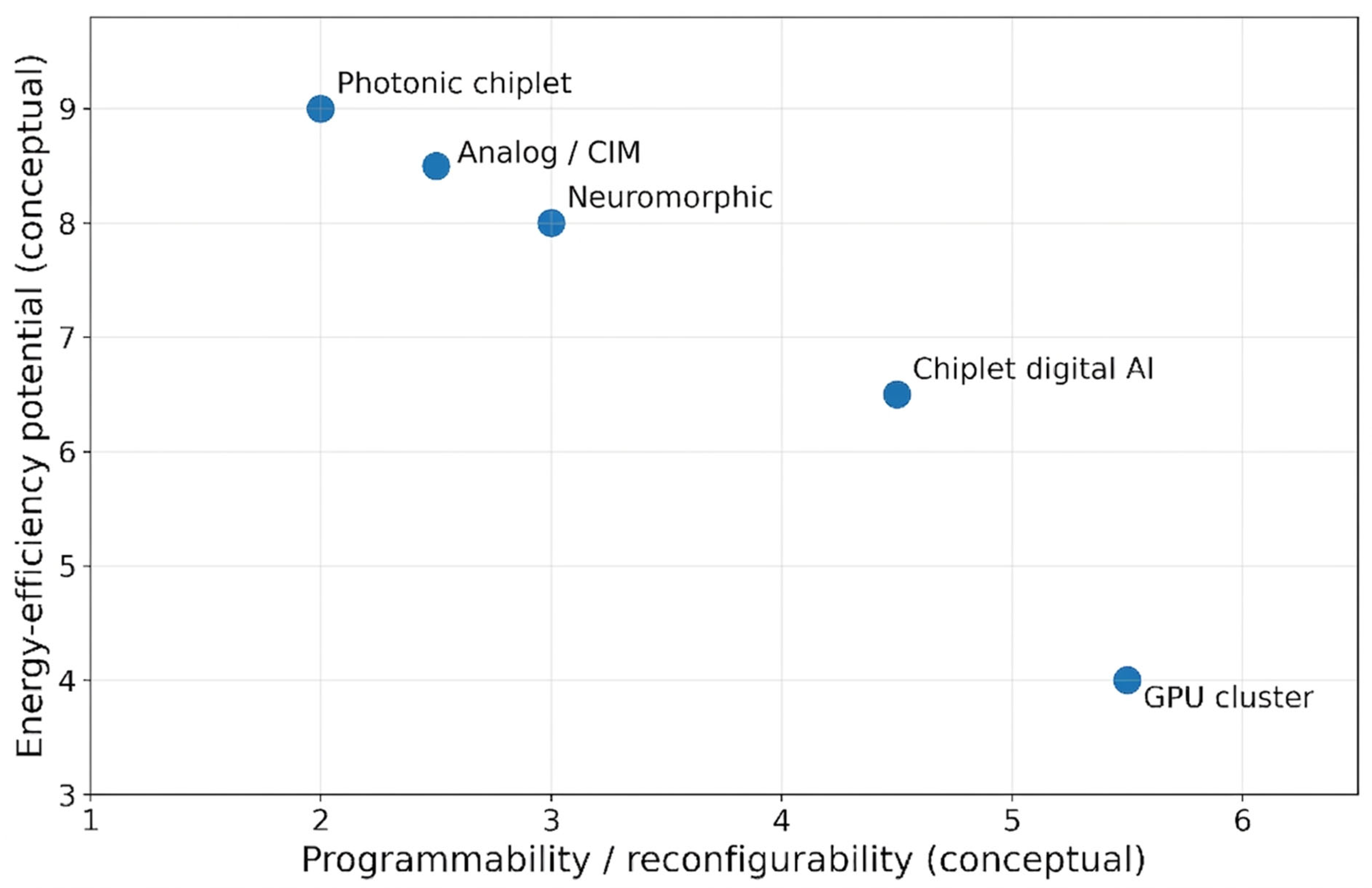
Even so, neuromorphic and mixed-signal platforms remain specialized rather than universally dominant. Their limitations include analog non-idealities, device variation, precision control, algorithm-to-hardware mapping complexity, software immaturity, and a narrower workload envelope than digital GPUs or NPUs [56,57,58,59,60]. Figure 11 summarizes this design space conceptually: conventional GPU clusters occupy a region of relatively high programmability but lower energy-efficiency potential, while analog/CIM, neuromorphic, and photonic approaches tend to move toward higher energy-efficiency potential but lower general-purpose programmability. Chiplet-based digital AI sits between these extremes, offering strong scalability and packaging flexibility without the same post-fabrication reconfigurability as FPGA-like platforms. The figure should therefore be read as a conceptual map rather than a benchmark ranking [55,56,57,58,59,60].
Overall, heterogeneous chiplet systems and neuromorphic or mixed-signal chips represent two complementary strategies for extending AI hardware beyond the limits of monolithic digital accelerators. Chiplet architectures primarily target scalability, modularity, and memory bandwidth, whereas neuromorphic, analog, compute-in-memory, and photonic approaches primarily target energy efficiency and data-movement reduction. Future AI platforms may increasingly combine both directions, assembling heterogeneous digital, memory-centric, analog, and photonic subsystems within the same package to balance performance, efficiency, and workload specialization [55,56,57,58,59,60].

4. Network-on-Chip (NoC) Architectures for AI Workloads

As AI accelerators have grown from relatively localized processing arrays into many-core and multi-chip systems, the interconnect has become a first-order architectural concern rather than a secondary implementation detail. In contrast to conventional CPU-oriented workloads, AI inference and training engines often generate highly structured traffic with substantial data reuse, repeated broadcasts of weights or activations, and bursts of reduction traffic for partial sums. Consequently, NoC design for AI chips must be evaluated not only in terms of average bandwidth and latency, but also in terms of multicast efficiency, locality support, energy cost of data movement, and the ability to sustain communication between shared buffers and spatial compute arrays [31,32,33,34,61].

4.1. Communication Patterns in AI Chips

4.1.1. Multicast-Heavy Neural Workloads

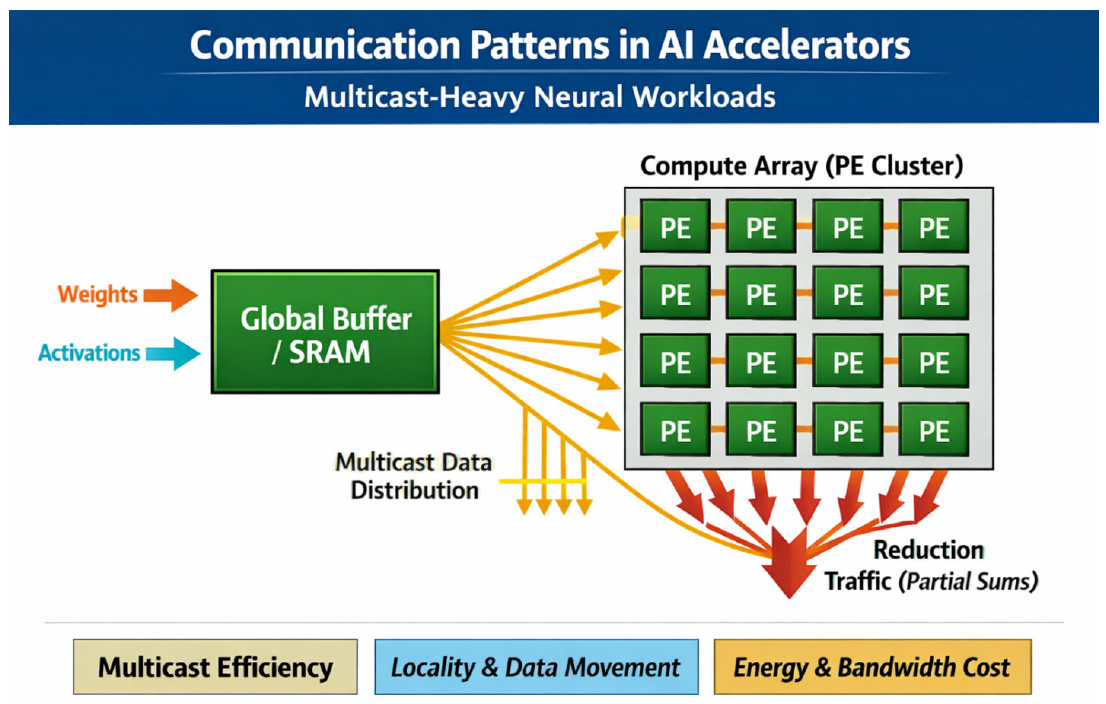
A defining property of many AI accelerators is that the same weights or activations are reused across multiple processing elements (PEs), which makes traffic patterns inherently multicast-heavy rather than uniformly point-to-point. This is evident in spatial architectures such as Eyeriss, where dataflow is organized to minimize movement across the memory hierarchy and maximize reuse within the PE array [31,33]. It is also explicit in the mTREE work, which states that AI-chip NoCs must often deliver data to multiple destination endpoints simultaneously and therefore require hardware support for multicast traffic rather than only conventional unicast routing. As illustrated conceptually in Figure 12, this creates a one-to-many communication pattern in which a shared global buffer or higher-level storage structure fans out data to many compute nodes [34].
This multicast behavior matters because AI traffic is strongly shaped by dataflow. In convolutional and matrix-oriented workloads, the accelerator attempts to reuse ifmaps, weights, and partial sums as close to the compute fabric as possible. Eyeriss and its later variants explicitly optimize data movement over a multi-level storage hierarchy, while Eyeriss v2 introduces a hierarchical mesh NoC to adapt to varying reuse and bandwidth requirements across different DNN layers. The implication is that NoCs for AI cannot be designed under the assumption of random or homogeneous traffic. Instead, they must support repeated fan-out from memory structures to arrays, as well as selective local exchange among neighboring Pes [33,61].

4.1.2. Global Buffer-to-Compute-Array Traffic

A second recurring pattern is the dominant traffic path between a global buffer and a compute array. In many AI accelerators, the global buffer acts as an intermediate staging point between off-chip memory and the PE array, while local register files or scratchpads serve as the innermost storage tier. Eyeriss v2 describes its hierarchical mesh NoC precisely in this context: the NoC connects a high-bandwidth global buffer to the PE array in a two-level hierarchy so that bandwidth delivery and data reuse can both be preserved across varying workloads. Similarly, the research in [32] describes a large software-managed on-chip memory serving a systolic compute fabric, emphasizing that practical throughput depends on keeping the compute array supplied with data from the memory hierarchy [61].
For this reason, the main interconnect problem in AI accelerators is often not generic core-to-core messaging, but structured delivery from shared storage to many compute endpoints. Figure 13 summarizes this communication style conceptually, while Table 6 compares how representative AI-oriented NoC designs respond to it. Architectures that ignore this access pattern risk underutilizing compute resources because arithmetic throughput is lost whenever the NoC cannot deliver shared operands efficiently to the array [32,33,34].

4.2. Multicast-Optimized NoC Designs

4.2.1. Tree-Based Versus Mesh-Based NoCs

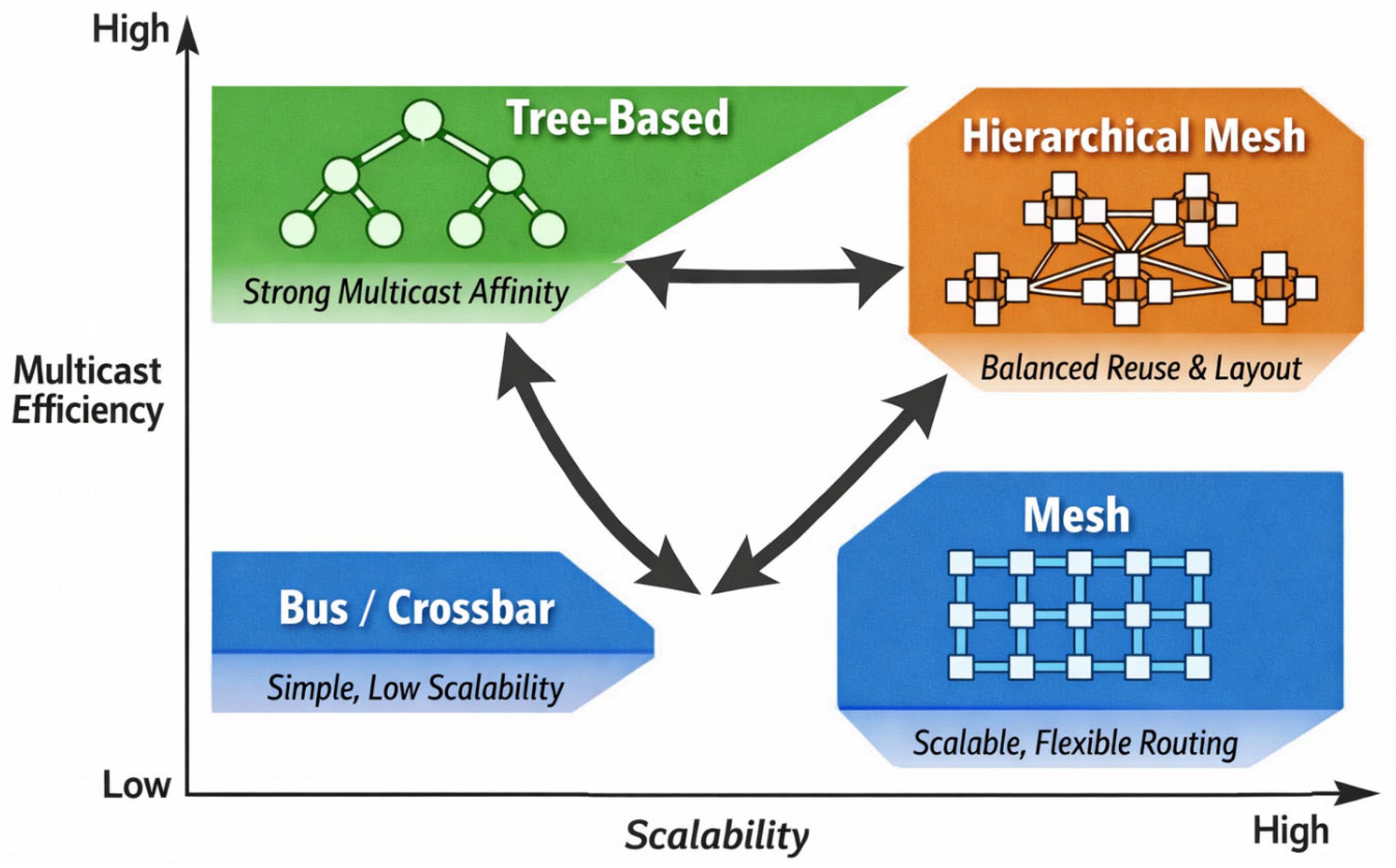
Because AI traffic often contains one-to-many data delivery, NoC topologies that are adequate for conventional many-core processors may not be optimal for DNN accelerators. Mesh-based NoCs are attractive because they scale well and naturally fit physical floorplans, but pure meshes do not always handle multicast traffic efficiently without additional support. Eyeriss v2 addresses this by using a hierarchical mesh that adapts to the bandwidth and reuse requirements of different data types and DNN layer shapes [34]. By contrast, the mTREE design takes a tree-based approach and modifies router microarchitecture specifically to support multicast delivery in AI chips [34,61]. Thus, the comparison is not simply “tree versus mesh” in the abstract, but rather whether the topology and router design align with AI-style reuse and fan-out patterns.
This tradeoff is shown conceptually in Figure 14. Tree-based designs tend to align naturally with broadcast and multicast distribution, while mesh-based designs often offer stronger general scalability and routing flexibility. Hierarchical meshes attempt to bridge these properties by retaining mesh-like scalability while introducing structure that better supports shared-data delivery from upper memory levels to clustered compute resources [61]. For AI accelerators, the most effective topology is therefore often the one that balances multicast efficiency against implementation cost and floorplan practicality rather than the one that maximizes only generic bisection bandwidth [34,61,62].

4.2.2. Energy and Area Tradeoffs

The main reason multicast-aware NoC design matters is that communication energy and router overhead can quickly dominate system efficiency. In the mTREE design is especially useful here because it quantifies the benefit of specializing the router microarchitecture for multicast traffic rather than simply adding more routing resources. In that study, the designs were implemented on an Intel (now Altera) Arria 10 FPGA, a 20 nm mid-range FPGA platform often used for prototyping and comparative hardware evaluation, as it provides substantial logic capacity and high-performance programmable interconnect resources. Using the same FPGA target makes the area and resource comparisons more meaningful across NoC variants. The paper compares mTREE against both a multicast-enabled FATTREE NoC and a hierarchical-mesh alternative. Here, FATTREE refers to a tree-derived topology in which links or upper levels are “fatter,” i.e., provisioned with greater connectivity or bandwidth to better support aggregation and fan-out traffic than a simple tree. Such topologies are attractive for multicast because tree structures align naturally with one-to-many delivery, but they can also require more routers, links, or routing resources, which increases area and power overhead. Under this Arria 10 implementation, mTREE reportedly increased resource utilization by only about 1% relative to a traditional tree NoC, while reducing resource utilization and energy substantially compared with multicast-enabled FATTREE and hierarchical-mesh alternatives. These results reinforce a broader architectural lesson: in AI NoCs, specialization at the router and topology levels can be more effective than brute-force provisioning of additional interconnect structure [29].
At the same time, mesh-derived topologies remain important because physical implementation, wire length, and modular extensibility favor regular layouts. This is why many practical AI accelerators employ mesh, hierarchical mesh, or clustered mesh-like organizations rather than purely logical trees. Figure 14 can therefore be interpreted as a conceptual design-space map: bus or crossbar structures sit low on scalability, tree-based designs offer strong multicast affinity, hierarchical meshes balance structured reuse with layout practicality, and conventional meshes remain attractive for larger many-core organizations [29,31,34,35].

4.3. NoC-SoC Co-Integration for AI Systems

4.3.1. Scalability Limits of Bus-Based SoCs

A recurring theme in the literature is that bus-based SoCs become increasingly inadequate as AI systems integrate more compute blocks, memory clients, accelerators, and I/O endpoints. Recent NoC surveys note that traditional bus or crossbar organizations struggle with scalability, bandwidth pressure, and predictable latency as core counts grow, especially in heterogeneous systems [34,35]. The uploaded paper on SoC optimization with AI and SDN makes a similar argument at the architectural level, stating that SoC alone is not sufficient to support dense-core hardware and that NoC must be blended with SoC to handle more cores and threads effectively. In other words, NoC is no longer just a replacement for a bus; it is an enabling infrastructure for heterogeneous AI SoCs [34,35].
For AI-specific platforms, this matters because the system integrates more than compute alone. A modern AI SoC may combine NPUs, CPUs, DSP blocks, global buffers, memory controllers, compression engines, security logic, and sensor or networking interfaces. Once these blocks scale beyond a modest number, the interconnect must provide both throughput and isolation. This is why Table 6 distinguishes bus/crossbar designs from NoC-enabled organizations: the former may remain acceptable for smaller or tightly scoped systems, but they do not scale gracefully to many-core AI fabrics or heterogeneous packages [34,35].

4.3.2. NoC-Enabled Many-Core AI Chips

NoC-enabled AI chips push this logic further by treating the compute fabric, memory hierarchy, and interconnect as a co-designed system. Eyeriss, Eyeriss v2, and TPU-style accelerators all show that the interconnect is inseparable from the dataflow and storage hierarchy. At a larger scale, the Simba work extends this idea into a multi-chip setting, showing that deep-learning inference can be scaled with fine-grained chiplets, with each chiplet delivering 4 TOPS and the 36-chiplet package reaching up to 128 TOPS and 6.1 TOPS/W. Although Simba operates at package scale, it reinforces the same design principle as many-core NoCs: AI performance depends on orchestrating communication among distributed compute and memory resources, not merely on adding more MAC units [32,33,35,61].
Accordingly, NoC-enabled many-core AI chips should be understood as communication-centric spatial systems. Their scalability is bounded by how well the interconnect supports buffer-to-array traffic, data reuse, multicast delivery, and local reduction. This is why NoC design increasingly appears alongside dataflow design and memory hierarchy design in AI accelerator papers rather than as an isolated backend concern [7].

4.4. NoC-Enabled Edge and IIoT AI Systems

4.4.1. Predictive Maintenance and Fault Diagnosis

NoC ideas are not limited to high-end training accelerators; they are also increasingly relevant in edge and industrial AI systems, especially where real-time sensing, multiple signal sources, and embedded inference must coexist. A recent IIoT fault-diagnosis and notification system provides a representative example by integrating a wireless smart machine box, an edge-AI fault-diagnosis flow, and a NoC-DNN AI chip with a Xilinx PYNQ-ZU platform to support real-time predictive maintenance in an industrial environment. This is significant because predictive-maintenance workloads often require near-continuous sensing, feature extraction, classification, and notification, which means the edge platform must sustain both data ingestion and inference under tight latency constraints [6].
This use case also clarifies why NoC matters at the edge. In predictive-maintenance systems, data does not flow only from memory to an inference core; it must also move between sensors, embedded processors, buffers, AI engines, and network interfaces. A NoC-enabled design offers a structured way to coordinate those flows while avoiding the congestion and poor scaling of simpler shared-interconnect schemes. Thus, the role of NoC in industrial AI is not only to accelerate DNN kernels but also to support system-level concurrency across sensing, diagnosis, and response [6,62].

4.4.2. Real-Time Industrial AI Platforms

The broader literature on industrial fault diagnosis shows why this architectural direction is valuable. Recent studies emphasize that predictive maintenance and industrial condition monitoring increasingly depend on data-driven pipelines that must operate reliably on streaming vibration, acoustic, or operational data, often with limited tolerance for latency or connectivity loss. For such systems, pushing inference to the edge reduces response time and dependency on remote infrastructure, but it also increases the need for efficient on-chip communication among heterogeneous modules. In this setting, NoC becomes part of the real-time platform architecture rather than only an internal accelerator optimization [6].
Overall, recent work on IIoT fault diagnosis and the broader NoC literature point in the same direction: NoC-enabled edge AI platforms are becoming attractive for industrial environments because they combine scalable interconnects, embedded inference capability, and system-level modularity. As industrial AI platforms grow to support more sensors, richer models, and tighter real-time constraints, their performance will increasingly depend on the same NoC principles that already shape many-core AI chips: multicast efficiency, memory-hierarchy awareness, and scalable integration of heterogeneous processing elements [4,6,63].

5. AI Model Acceleration and Algorithm–Hardware Co-Design

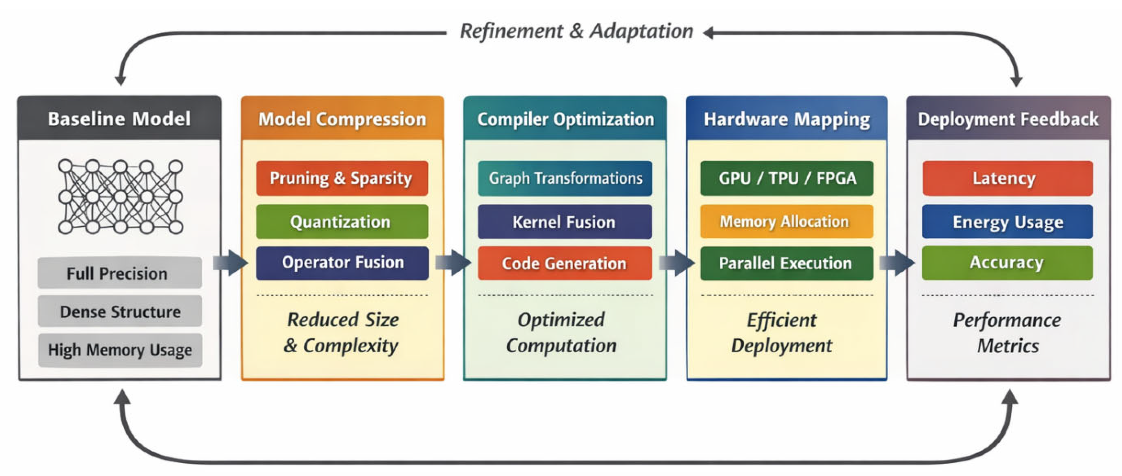
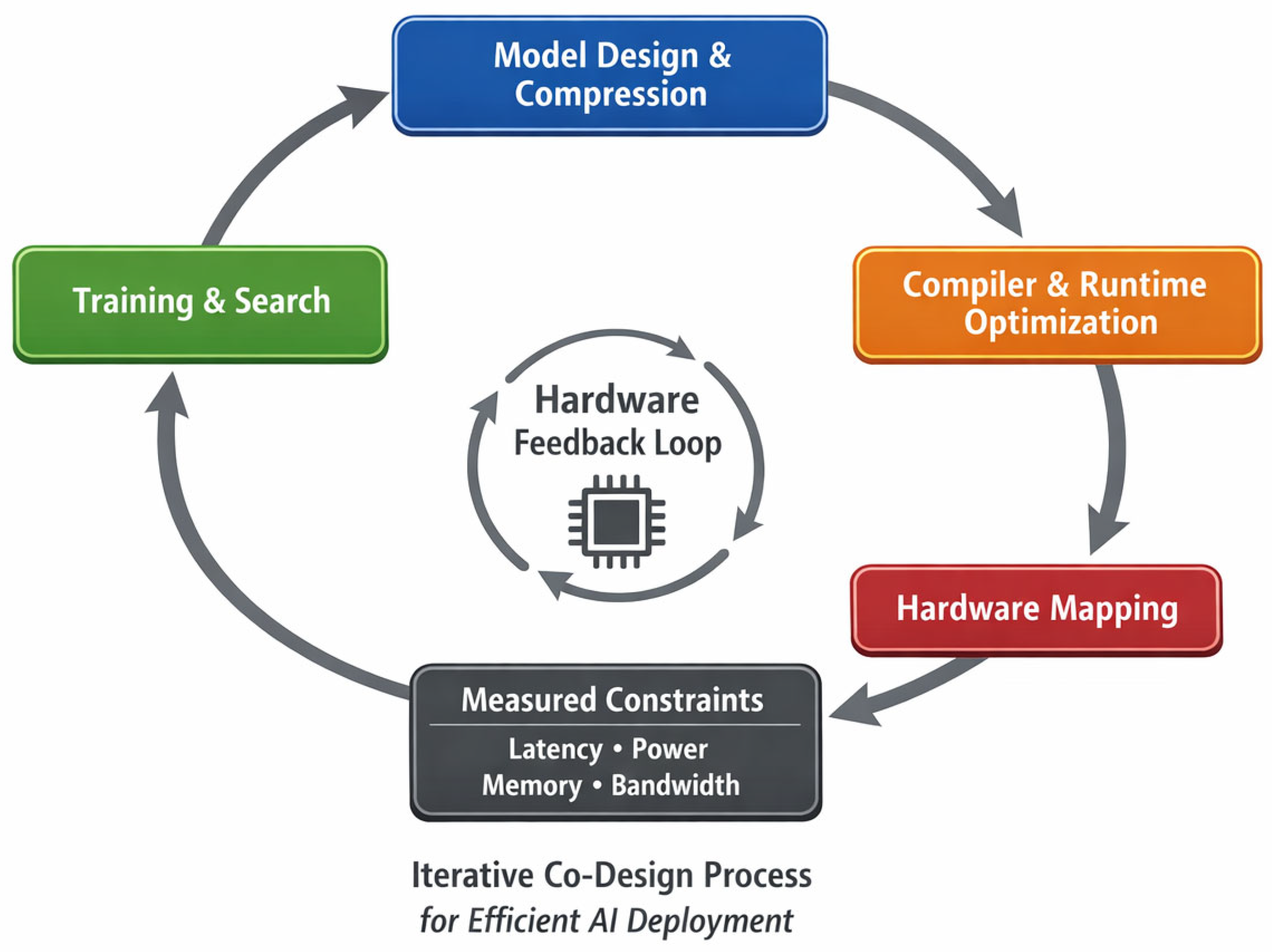
AI acceleration is no longer determined by hardware throughput alone. In modern deployment pipelines, latency, energy, memory footprint, and achievable accuracy are jointly shaped by model structure, numerical precision, compiler transformations, and the target execution substrate. As a result, high-performance AI systems increasingly rely on algorithm–hardware co-design, in which compression, quantization, fusion, architecture search, and runtime scheduling are optimized together rather than in isolation. This full-stack perspective is summarized conceptually in Figure 15, which shows how a baseline model is progressively transformed through compression, compiler optimization, and hardware mapping, then refined again through measured deployment feedback [64,65,66,67,68,69,70,71,72].

5.1. Model Compression and Quantization

Pruning, Quantization, and Operator Fusion

Model compression remains one of the most influential pathways for practical AI acceleration because it directly reduces the memory traffic and arithmetic intensity that often dominate real deployments. In the classic Deep Compression pipeline, combined pruning, trained quantization, and Huffman coding, and reported that AlexNet, an early landmark CNN, could be compressed by 35×, and VGG-16, a deeper 16-layer CNN, by 49× without accuracy loss; the resulting compressed models also showed 3×–4× layerwise speedup and 3×–7× better energy efficiency on CPU, GPU, and mobile GPU platforms. These results are important because they demonstrate that compression is not merely a storage optimization; it can shift a model from off-chip DRAM dependence toward on-chip SRAM residency, thereby changing the effective hardware bottleneck itself [72]. Pruning, however, is only hardware-efficient when its sparsity structure aligns with the execution substrate. Unstructured pruning can produce high nominal sparsity, but it often maps poorly to dense tensor engines and conventional memory-access patterns. By contrast, structured pruning and architecture-aware simplification tend to translate more directly into measured gains on GPUs, NPUs, and FPGAs because they reduce channels, filters, blocks, or layers in ways that match hardware granularity This is one reason why recent hardware-aware compression methods increasingly optimize for direct deployment metrics such as latency and energy rather than proxy metrics such as parameter count or FLOPs (floating-point operations), which are commonly used to estimate computational cost alone [66,68].
Quantization provides a second major axis of acceleration. In [71], It is shown that neural networks can be quantized and trained for integer-arithmetic-only inference, allowing deployment on integer-oriented hardware while largely preserving end-to-end accuracy. Their results were especially influential because they framed quantization not simply as post-processing, but as a training-and-deployment co-design problem: scale factors, activation ranges, and inference arithmetic all need to be coordinated with the target hardware format. Later work extended this logic to mixed-precision quantization, where different layers are assigned different bit widths according to measured hardware benefit. In HAQ, Wang et al. used hardware feedback inside the search loop and reported 1.4×–1.95× latency reduction and 1.9× energy reduction relative to fixed 8-bit quantization, with negligible accuracy loss [67].
A third important optimization layer is operator fusion, which reduces kernel-launch overhead, intermediate memory traffic, and redundant tensor movement. TVM, an automated end-to-end deep-learning compiler framework, formalized optimization at both graph and operator levels, explicitly supporting high-level fusion, mapping to diverse hardware primitives, and memory-latency hiding across CPUs, GPUs, FPGAs, and ASICs [70]. Subsequent analysis of XLA (Accelerated Linear Algebra), a compiler system for optimizing machine-learning computation graphs, showed that kernel-fusion decisions can materially change execution behavior and demonstrated fusion strategies yielding up to 10.56× speedup over a baseline implementation in the evaluated setting. In practical inference stacks, this means that hardware acceleration depends not only on the numerical precision of operators, but also on whether the compiler and runtime layers can combine operator sequences into execution units that reduce intermediate memory traffic and launch overhead [69].
Figure 15 can be read as a deployment pipeline rather than a strict chronology: compression changes the computational graph, compiler transformations exploit the new graph structure, hardware mapping exposes actual bottlenecks, and those measured bottlenecks then feed back into further model redesign. Table 7 summarizes the main compression and optimization techniques discussed in this subsection and highlights the deployment metrics they most directly influence.

5.2. CNN and Object Detection Acceleration on AI Chips

5.2.1. YOLO-Family Optimizations

Object detection is a particularly revealing case for algorithm–hardware co-design because the workload contains both regular dense convolution and irregular stages such as feature fusion, box decoding, and non-maximum suppression (NMS). The YOLO (You Only Look Once) family is central here because it was designed around real-time operation and has evolved through repeated speed–accuracy tradeoffs rather than accuracy maximization alone. YOLOv4 reported 43.5% AP (average precision) on the COCO (Common Objects in Context) benchmark at roughly 65 FPS (frames per second) on Tesla V100, while emphasizing a combination of architectural choices and “bag-of-freebies” training techniques such as CSP (Cross Stage Partial) connections, Mosaic augmentation, Mish activation, and CIoU (Complete Intersection over Union) loss, which improves bounding-box regression by jointly accounting for overlap area, center distance, and aspect-ratio consistency [73]. Scaled-YOLOv4 extended this design logic in both directions, reporting 55.5% AP at approximately 16 FPS for YOLOv4-large on Tesla V100 while also presenting a YOLOv4-tiny operating point of 22.0% AP at 443 FPS on RTX 2080Ti; with TensorRT, batch size 4, and FP16 precision, the paper reported 1774 FPS for YOLOv4-tiny [74]. YOLOv7 continued this trend and reported 56.8% AP among real-time detectors operating at 30 FPS or higher, while the YOLOv7-E6 configuration was reported at 55.9% AP and 56 FPS. These representative operating points are plotted in Figure 16, which makes visible the core deployment tradeoff between inference throughput and detection accuracy [73,74,75].
The main lesson from the YOLO lineage is that detector acceleration is not achieved by pruning a fixed architecture alone. Instead, the detector itself is progressively redesigned to reduce data motion, simplify feature reuse, and maintain favorable execution behavior on available inference engines. This includes changes to backbone structure, feature pyramid connectivity, convolutional blocks, detection heads, and post-processing. As a result, YOLO-family optimization is a model-level example of the same principle seen in Section 5.1: deployment efficiency emerges when algorithmic structure and hardware execution characteristics are considered jointly rather than sequentially [73,74,75].

5.2.2. Heterogeneous Acceleration Strategies

On actual AI chips, object detection is rarely executed as a single homogeneous kernel. A more common deployment pattern is heterogeneous acceleration, where different parts of the pipeline are assigned to different compute resources according to their structure. Dense convolutions and tensor-heavy feature extraction typically map well to GPUs, NPUs, or systolic units, while control-oriented tasks, preprocessing, bookkeeping, and sometimes post-processing remain on CPUs or programmable logic. SATAY illustrates this by targeting YOLO models on FPGAs through a streaming, deeply pipelined, largely on-chip dataflow architecture generated by an automated toolflow [76]. In a different but complementary direction, recent CPU + NPU heterogeneous work on FPGA-based systems explicitly treats object detection as a partitioned workload in which different subsystems cooperate rather than attempting to force the whole graph into one execution style [77].
A major reason heterogeneous execution matters is that the bottleneck in object detection often shifts away from convolution itself. Post-processing can become a serial bottleneck even when the main CNN is highly optimized. This was demonstrated clearly in high-throughput FPGA object detection work, where a pipelined NMS algorithm removed the sequential dependency of conventional NMS and enabled an end-to-end, fully pipelined SSD-MobileNet-V1 system on an Intel Stratix 10 FPGA. The reported system achieved 2167 FPS at 2.13 ms batch-1 latency and was reported as 5.3× higher in throughput and 5× lower in latency than the best prior comparable FPGA solution. This is a strong example of why object detection acceleration must include both the neural backbone and the surrounding algorithmic stages [78].
Accordingly, Table 8 summarizes representative acceleration strategies for CNN and object-detection workloads. The table highlights that the best deployment strategy depends on where the dominant cost resides. Convolution-heavy backbones benefit from low-precision tensor acceleration, while graph irregularity, buffering, and NMS overhead often call for compiler support, streaming architectures, or heterogeneous task partitioning.

5.3. Algorithm-Architecture Co-Design Methodologies

5.3.1. Hardware-Aware Neural Network Design

The broader methodological shift behind the preceding results is that efficient AI models are increasingly designed for hardware, not merely compressed after training. This idea appears in several forms. NetAdapt uses measured latency and energy in the adaptation loop rather than relying on indirect structural metrics, and reported up to 1.7× speedup on mobile CPU/GPU platforms for MobileNet variants while maintaining favorable accuracy–latency tradeoffs [66]. ProxylessNAS, which stands for neural architecture search, moved architecture search closer to the target hardware and reported ImageNet architectures that were 1.2× faster than MobileNetV2 with higher top-1 accuracy in the evaluated hardware setting. FBNet, similarly, used differentiable search with measured operator latency on the target device rather than FLOPs (floating-point operations) alone, reinforcing the point that hardware-aware design should optimize the metric that deployment actually experiences [64,65,66].
Once-for-All (OFA) extends this logic into a reusable supernetwork paradigm. Rather than re-running the architecture search for every deployment target, OFA trains a once-for-all network and then specializes subnetworks for different resource constraints. The paper reports that OFA can match or exceed the state of the art on diverse edge devices, including up to 4.0% ImageNet top-1 improvement over MobileNetV3, or the same accuracy at 1.5× faster measured latency than MobileNetV3 and 2.6× faster than EfficientNet in the reported comparisons. This matters because it reframes hardware-aware design as a scalable deployment process instead of a one-off search exercise [64].

5.3.2. Precision and Sparsity Co-Design

A second methodological theme is the co-design of precision and sparsity. The central issue is that numerical precision, activation statistics, weight sparsity, and memory layout are all entangled at deployment time. HAQ, which stands for Hardware-Aware Automated Quantization, showed this explicitly by using hardware feedback to choose layerwise precision policies that differ across edge and cloud targets [67]. Likewise, sparse-Winograd work demonstrated that sparsity and fast convolution transforms cannot simply be stacked naively; they must be reformulated together so that the transformed domain still exposes useful sparsity. In the reported results, the proposed method reduced the number of multiplications by 10.4×, 6.8×, and 10.8× on CIFAR-10 (Canadian Institute for Advanced Research 10-class dataset), CIFAR-100 (100-class version of the same benchmark), and ImageNet models, respectively, with accuracy loss under 0.1%. This is a strong example of co-design because both the algorithmic transform and the sparsity pattern were changed to make the optimization hardware-meaningful [79].
Figure 17 emphasizes model design, compression, compiler/runtime optimization, hardware mapping, and measured constraints form a closed loop rather than a linear pipeline. In practical AI-chip development, this means that deployment metrics such as latency, SRAM (static random-access memory) pressure, bandwidth, and power become training-time or search-time design inputs. Table 9 summarizes the main co-design methodologies discussed in this subsection and clarifies how each one integrates hardware feedback into algorithmic choices [64,65,66,67,79].

6. Clocking, Synchronization, and Timing in AI Chips

As AI chips continue to scale in die size, memory bandwidth, and heterogeneity, clocking and synchronization have become central architectural concerns rather than purely back-end implementation details [80,81,82,83,84,85,86,87]. Modern AI SoCs increasingly combine high-frequency compute arrays, large on-chip SRAM or global buffers, HBM/PHY interfaces, and peripheral or control subsystems that do not naturally operate at the same frequency or voltage [80,81,86]. At the same time, chiplet-based integration shifts some timing problems from intra-die routing to inter-chiplet coordination [82,83,84]. IBM’s processor clocking overview emphasizes that high-performance chips increasingly rely on more specialized global clocking methods such as spines and meshes because simple trees alone become less robust as skew, power, and design-closure pressures grow. In parallel, recent chiplet studies treat package-level timing, die-to-die signaling, and local clock generation as co-equal parts of system design rather than as separate implementation stages [82,83,84].

6.1. Clock Distribution Challenges

6.1.1. Large Die Sizes and Skew Management

Clock distribution becomes harder as die dimensions grow because the physical distance from the clock source to distant sinks increases, making the network more sensitive to wire delay, process variation, voltage droop, and local loading imbalance [80,84]. IBM’s processor clocking discussion notes that modern high-performance processors often move beyond simple trees to spines, meshes, and resonant structures because these approaches offer improved skew tolerance, robustness, and timing closure compared with more conventional clock trees alone [80]. This is directly relevant to AI chips, whose large compute fabrics and memory subsystems create long clock paths and substantial sink counts. As illustrated conceptually in Figure 18, once the chip contains multiple large functional regions, clock distribution is no longer a single uniform fan-out problem, but a timing network spanning compute, memory, control, and I/O blocks with different loading and synchronization requirements [80,81,82].
Skew management is particularly important in AI accelerators because timing margin is often already stressed by aggressive frequency targets and dense arithmetic pipelines [80,83]. In large-array designs, even modest skew or jitter can reduce useful timing headroom across the multiply–accumulate fabric and memory interfaces [80]. Earlier multi-clock-domain processor work showed that one reason to partition a large processor into multiple clock domains is precisely to reduce the burden of global skew closure; in that framework, each local domain receives a reference and generates its own clock, thereby relaxing the requirement for one globally balanced clock network. Although that work predates modern AI accelerators, the architectural lesson remains highly relevant: very large synchronous domains become increasingly expensive to clock cleanly, both electrically and physically [86,87].

6.1.2. Multi-Clock-Domain AI Systems

Most practical AI SoCs are now multi-clock-domain systems [81,86]. Control logic, memory controllers, PHYs, on-chip networks, NPUs, and peripheral interfaces frequently operate at different frequencies for performance, power, or IP-integration reasons. In [81], the draft standard reflects this reality by formalizing explicit clock-group relationships and by treating asynchronous or partially synchronous interactions as a default verification concern rather than an edge case. It also highlights common failure modes such as missing synchronizers and reset-domain issues, both of which are especially relevant when AI chips combine many reusable IP blocks and multiple generated clocks. In other words, moving to many domains simplifies some aspects of local clock closure, but it introduces clock-domain crossing (CDC) and synchronization risk at the architectural level [81,85,86].
This is why Figure 18 includes dashed inter-domain paths: in AI hardware, timing challenges arise not only inside a compute array, but also wherever data crosses between control, memory, accelerator, and I/O domains [81,85]. These boundaries usually require synchronizers, elastic buffering, FIFOs, or carefully constrained handshake protocols. Prior work on multi-clocked processors observed that inter-domain synchronization overhead can increase cycle count or latency even when the clock network itself becomes easier to manage. For AI chips, this creates a familiar tradeoff: finer-grained clock partitioning improves local timing and power management, but it can also increase synchronization latency and verification complexity [81,85,86,87].
Table 10 summarizes the main clock-distribution challenges that arise in large AI dies and multi-domain systems.

6.2. Clock Trees for Heterogeneous AI Chiplets

6.2.1. Energy-Aware Clocking Techniques

For heterogeneous AI chiplets, the clock network must be designed not only for skew, but also for energy efficiency [80,84,85]. Clock power remains significant because the clock toggles every cycle, drives large capacitive trees, and reaches nearly every sequential element [80]. As a result, clock gating remains one of the most important dynamic-power-reduction techniques in digital systems [80,85]. IBM’s processor clocking review explicitly discusses clock gating, useful skew, and specialized global clock structures as part of practical high-performance clock design [80], while CDC-aware sequential clock-gating work shows that power savings must be balanced against the risk of introducing unsafe inter-domain behavior. That work reported an average 22% sequential power savings when clock-gating optimization was made CDC-aware, reinforcing the point that energy-aware clocking cannot be separated from synchronization correctness [85].
For AI chips, energy-aware clocking is especially attractive because utilization is often nonuniform across layers, heads, engines, or memory slices [80,82]. This makes localized clock gating, domain-specific frequency selection, and partial shutoff more valuable than a monolithic always-on network [80,85]. The same logic extends naturally to chiplet systems: rather than distributing a single, aggressively tuned global clock everywhere, a more efficient strategy is often to distribute a cleaner global reference and let each chiplet perform local division, deskew, or gating based on its own workload and interface constraints. Figure 19 illustrates this idea conceptually by separating the package-level reference distribution from the chiplet-level clock specialization [83,84].

6.2.2. Modular and Hierarchical Clock Networks

Clocking methodology for chiplets is increasingly hierarchical and modular. In [84], it describes a 2.5-D clocking architecture for a 64-core heterogeneous system that explicitly separates interposer clocking from on-chiplet clocking. In that design, clocks used for global synchronicity and inter-chiplet communication are distinguished from clocks generated and managed locally within each chiplet. This distinction is important because passive interposers cannot be treated like ordinary active silicon: buffering options, transmission-line behavior, and impedance effects differ, so clock design must be aware of both package physics and chiplet-local timing closure.
This kind of hierarchy is becoming even more relevant as commercial AI systems move toward multi-chiplet organization. In [83], it shows a quad-chiplet AI SoC with a scalable full-chip mesh over a 16 Gb/s UCIe-Advanced die-to-die interface for large-scale AI inferencing, indicating that package-scale AI clocking and synchronization are now mainstream enough to appear in flagship silicon venues. Although the program entry does not provide full clock-network details, it strongly supports the broader trend: AI chiptiming is shifting from purely intra-die clock-tree synthesis toward combined die-to-die timing, package-level coordination, and local chiplet clock specialization [83,84].
A modular clocking strategy also fits the architecture of heterogeneous systems more naturally than a flat tree [80,84]. Compute chiplets may prefer high-frequency local trees or meshes, cache/SRAM chiplets may prioritize low-skew regional distribution, and PHY or I/O chiplets may align their clocking to interface timing constraints rather than core-array frequency. For this reason, Figure 19 shows more than a packaging diagram: it represents a design principle in which stable package-level coordination is preserved while each chiplet retains enough local autonomy to optimize skew, power, and domain specialization. Table 11 summarizes these modular clocking choices and their associated tradeoffs [82,83,84].

7. AI for Chip Design and Design Automation

AI is increasingly being used not only inside AI chips, but also to design them. In EDA, AI methods now support early analysis, optimization, code generation, and increasingly autonomous design loops that operate across multiple tools and abstraction levels [88,89,90,91,92,93,94]. Recent surveys describe this shift as a move from narrow AI for EDA point solutions toward broader foundation-model and agentic workflows that can reuse prior design data, reason across heterogeneous representations, and shorten turnaround time across architecture, register-transfer level (RTL), physical design, and verification stages [95,96,97]. The same surveys also emphasize that modern EDA problems are especially well-suited to AI, as many downstream analyses remain computationally expensive, while historical design data can often be leveraged to build useful predictors and optimizers. This broader closed-loop view is illustrated in Figure 20, where prediction, optimization, and measured design feedback form a recurring cycle rather than a one-shot tool invocation [88,93,97,98].

7.1. AI-Assisted Analysis in Chip Design

Timing, IR-Drop, and Congestion Prediction

One of the most mature uses of AI in chip design is early prediction of downstream implementation metrics. Instead of waiting for expensive sign-off or near-sign-off analyses, machine-learning models can estimate timing, routing congestion, or power-integrity risk much earlier in the flow, allowing poor design choices to be filtered out before costly iterations accumulate. It is shown that machine-learning models could achieve prediction accuracy close to post-routing timing analysis while reducing the pessimism of conventional early timing estimation. The core idea was to learn delay behavior from known placed-and-routed designs, then apply that knowledge at the placed-but-unrouted stage to guide optimization earlier in the flow [88,89,90,91,92].
A similar motivation appears in IR-drop prediction. In [89], it describes IR drop as a fundamental chip-design constraint whose evaluation is time-consuming and often requires many iterative fixes; it argues that fast and accurate prediction is therefore critical for reducing design turnaround time. It also reviews how ML-assisted IR-drop estimation can be integrated with conventional EDA techniques rather than replacing them outright, which is a good example of how AI tends to function in practice: as a surrogate model or prioritization layer inside a larger design flow [89].
Routing congestion prediction is another important analysis target because congestion affects routability, timing closure, and downstream power, performance, and area (PPA) [90,91,92]. Public datasets such as CircuitNet 2.0 have become influential precisely because they make these learning problems more reproducible: the dataset introduces more than 10,000 samples from diverse chip designs, including CPU, GPU, and AI-chip cases, and was explicitly created to support realistic EDA-oriented learning tasks [90]. Related work also reports large industrial-style samples for congestion prediction, including 150 samples generated from five-million-cell superblue designs by varying macro locations. Together, these efforts show why AI-assisted analysis is valuable: timing, congestion, and IR-drop can be predicted early enough to guide design decisions before full detailed optimization is invoked. This role is summarized in Table 12 and placed in workflow context by Figure 20 [88,89,90,91,92].

7.2. AI-Driven Optimization

Bayesian Optimization and Reinforcement Learning

Beyond prediction, AI is increasingly used to optimize chip design decisions directly [93,94,98,99,100,101,102]. Two especially visible paradigms are Bayesian optimization (BO) and reinforcement learning (RL). BO is attractive when design evaluation is expensive and derivative information is unavailable, which makes it well-suited to flow-parameter tuning, analog sizing, and macro-placement-style black-box objectives. Recent chip-design agent papers explicitly note that BO is already widely used for parameter autotuning in EDA, including commercial practice, because it is sample-efficient. At the same time, those same papers point out that BO has limitations in high-dimensional design spaces, requires explicit objectives, and typically incorporates domain knowledge only when it is manually encoded. A separate BO-based macro-placement study also showed that BO can be applied over sequence-pair representations for fixed-outline macro placement, making it a relevant alternative to classical heuristics for expensive placement objectives [93,98].
RL, by contrast, is appealing when chip design can be formulated as a long-horizon sequential decision process [94,99]. The most famous example is in [94] on graph placement for fast chip design, which posed chip floorplanning as a deep RL problem and reported floorplans generated in under six hours that were comparable or superior to human-produced layouts on the studied TPU-related blocks. That work was highly influential in motivating AI-driven physical design, but later reassessments argued that the public evidence for state-of-the-art performance was incomplete and that independent evaluations did not support the stronger claims that followed. The balanced conclusion is that RL-based floorplanning is historically important and methodologically influential, but its real-world advantage should be described carefully and not treated as universally settled across all benchmarks and industrial settings [94,99].
Recent work increasingly combines these ideas [93,98]. Rather than choosing between BO and RL in isolation, newer systems integrate predictive models, optimizer policies, and explicit tool feedback inside one loop [98]. Figure 20 captures this structure at a conceptual level: analysis models predict timing, congestion, or IR-drop; an optimization engine proposes changes; EDA tools execute those changes; and measured outcomes close the loop [88,89,93,98]. This is also why purely black-box optimization is giving way to more tool-aware optimization frameworks that exploit logs, domain metadata, and partial design-state information.

7.3. LLMs and AI Agents for Chip Design

7.3.1. RTL Generation and Design-Space Exploration

Large language models (LLMs) have opened a new front in chip-design automation because they can generate and transform structured code, constraints, and flow scripts from textual specifications [97,100,102,103]. Recent surveys of LLMs for EDA and of circuit foundation models describe this as a shift from narrow predictive models toward generative systems that can operate on RTL, netlists, scripts, verification artifacts, and natural-language design intent [95,97]. The resulting workflows are especially promising in front-end design tasks such as RTL generation, assertion generation, and design-space exploration (DSE), where the problem is partly symbolic and partly tool-constrained [95,100,102]. Figure 21 summarizes this agentic workflow: a natural-language or structured intent is converted into RTL or scripts, EDA tools evaluate the result, logs and quality-of-results (QoR) metrics are collected, and the model or agent revises its output accordingly [95,96,97,98,102,103].
The practical challenge, however, is correctness. Research on EDA-aware RTL generation emphasizes that zero-shot RTL code generation remains unreliable even for strong models and proposes a self-verifying multi-agent framework that uses EDA-tool error logs to iteratively repair syntax and functional issues [100]. On the reported benchmark, AIvril2 achieved nearly 3.4× improvement over prior methods, with best-case functional pass rates of 77% for Verilog and 66% for VHDL [100]. These results are noteworthy not only because they improve raw success rate, but because they demonstrate the importance of a tool-in-the-loop strategy: the LLM becomes more useful when it can observe simulator or verifier feedback rather than generating code once and stopping [100].
Benchmarking work reinforces the same message [95,102]. OpenLLM-RTL reports that the public benchmark has been expanded to 50 RTL designs, with associated test cases and a human-crafted reference RTL, and that it also introduces a larger training-data framework that includes an 80K-sample instruction-code dataset and a 7K-verified, high-quality subset [102]. Meanwhile, newer hardware-design benchmarks show that agentic tasks remain difficult even for strong models, and that realistic evaluation requires containerized tool use, verification harnesses, and more than simple text matching [95,102]. In other words, LLMs can already assist RTL design, but their usefulness depends heavily on benchmark realism, verification infrastructure, and access to debugging signals from the EDA stack. This is why Table 13 distinguishes plain LLM code generation from verification-aware and benchmark-driven workflows [95,100,102].

7.3.2. Autonomous EDA Workflows

The next step beyond LLM-assisted code generation is the rise of AI agents that orchestrate entire design flows [95,96,97,98]. Agentic EDA surveys define this as a transition from static “brain” models to “engineer” systems that can reason over tool outputs, launch commands, revise constraints, and navigate multistage flows more autonomously [95,97]. The 2025 ORFS-agent paper is a concrete example: it wraps OpenROAD-flow-scripts, uses OpenROAD as a transparent RTL-to-GDSII testbed, and positions the agent as a design-optimization layer that can use logs, APIs, and metrics rather than relying only on fixed prompts [98]. The paper explicitly contrasts this approach with standard BO, arguing that LLM-based agents can exploit contextual metadata and design knowledge that pure black-box optimization often ignores. More recent surveys frame this trend as Agentic EDA, emphasizing that autonomous workflows are likely to matter most when they combine classical solvers, foundation models, and tool-execution feedback rather than replacing EDA infrastructure outright. That broader trend is captured conceptually in Figure 21 [95,97].
At the same time, recent workshop and survey reports emphasize major limitations: lack of robust open datasets, limited industrial-grade benchmarks, significant compute cost, and persistent generalization gaps across nodes, tool stacks, and design styles The 2026 NSF workshop report is especially clear on this point, highlighting data availability, scalability, and open infrastructure as current showstoppers even while recommending major investment in AI/EDA collaboration. Thus, autonomous EDA workflows are best understood not as turnkey replacements for expert designers, but as emerging copilots and orchestration layers that may substantially reduce repetitive work, expand design-space coverage, and shorten iteration cycles when paired with trustworthy verification and optimization backends [95,96,97].
As AI chips scale in transistor count, memory bandwidth, and system-level heterogeneity, manufacturing and packaging increasingly define achievable performance, energy efficiency, and product lifetime [7,21,27,28,42,104,105]. Recent reviews emphasize that packaging is no longer a downstream enclosure problem; it has become a first-order architectural enabler for multimodal integration, high-bandwidth memory attachment, and heterogeneous chiplet scaling [7,21,27,28,104]. At the same time, reliability constraints such as microbump integrity, thermomechanical stress, void formation, and yield loss increasingly limit how aggressively advanced integration can be deployed in practice. This broader shift is reflected in both the AI-chip review literature and recent packaging-focused studies, which repeatedly identify 2.5D/3D integration, thermal bottlenecks, and interconnect reliability as central concerns for next-generation AI hardware [7,26,104,105,106].

8. Manufacturing, Packaging, and Reliability of AI Chips

8.1. Advanced Packaging for AI Chips

8.1.1. 2.5D and 3D Integration

A central packaging trend in AI hardware is the transition from monolithic dies toward 2.5D and 3D integration [7,26,104,105,106]. In 2.5D integration, multiple dies are placed side by side on a high-density interposer, typically silicon, to provide short, high-bandwidth links among compute chiplets, I/O dies, and high-bandwidth memory (HBM) [26,107]. In 3D integration, logic and/or memory dies are stacked vertically using through-silicon vias (TSVs) or hybrid-bonded interfaces, reducing interconnect length further and increasing bandwidth density [104,105,106]. Recent reviews note that 2.5D/3D packaging has become one of the principal means of extending chip performance beyond what is practical with monolithic scaling alone [7,26,104,105,106].
This shift is especially relevant to AI workloads because modern training and inference engines are dominated by memory traffic as much as by arithmetic throughput [7,26]. The NVIDIA co-optimization study makes this explicit at the system-product level: it describes 2.5D heterogeneous integration with HBM3E as a key contributor to large gains in performance per watt relative to more conventional architectures, while also emphasizing that leading GPU AI chips now combine enormous transistor counts with extreme packaging complexity [26]. At the broader review level, recent AI-chip surveys likewise frame packaging technique development as one of the main co-optimization dimensions alongside materials, circuits, and architecture [7].
Figure 22 summarizes this progression conceptually. The left side shows a monolithic die, where compute, memory, and I/O are confined to a single silicon footprint. The center shows a 2.5D organization, in which multiple compute dies and HBM are integrated through an interposer. The right side shows 3D stacking, where vertical integration further shortens communication paths. This architectural scaling path: bandwidth density and modularity generally improve from monolithic integration to 2.5D and 3D packaging, while thermal, mechanical, and manufacturing complexity also rise [7,26,104,105,106].
A particularly important enabling technology for dense 3D packaging is hybrid bonding, especially Cu–Cu or C u / S i O 2 -based hybrid bonding. Recent reviews describe hybrid bonding as a route to interconnect densities far beyond conventional solder microbumps, with lower resistance and stronger relevance to high-performance 3D integration. At the same time, these reviews emphasize that shrinking pad pitch and bonding dimensions introduce new process and reliability sensitivities. Thus, the packaging choice is not merely a matter of bandwidth; it directly affects assembly tolerance, thermal behavior, and long-term lifetime [106].

8.1.2. Thermal and Mechanical Considerations

Thermal and mechanical issues become more severe as packaging density increases [7,26,104,105,106]. The core reason is straightforward: 3D stacking improves communication locality by bringing logic and memory closer together, but it also raises volumetric power density and lengthens heat-removal paths from buried tiers. Recent reviews of 3D-stacked chips therefore emphasize that heat dissipation is one of the most visible and persistent bottlenecks in vertically integrated systems. These reviews identify vertical heat accumulation, nonuniform temperature fields, and difficulty in cooling internal tiers as recurrent barriers to wider deployment [104].
Mechanical reliability is closely coupled to the thermal problem [42,104,107]. Temperature gradients and repeated thermal cycling generate stress because the constituent materials in an advanced package—silicon, copper, underfill, molding compounds, organic substrates, and solder or hybrid bonds—have different coefficients of thermal expansion [104,107]. Recent studies and reviews show that these stresses can drive warpage, delamination, cracking, and microbump fatigue, especially in thin dies and densely stacked structures [42,104,107]. Reliability work on ultrathin 3D-IC packages and on 2.5D package manufacturing, similarly, shows that residual thermomechanical stress from assembly can materially affect later thermal-cycling reliability [104,107].
This is why thermal and mechanical design cannot be separated cleanly in AI packaging. The package must simultaneously provide high-bandwidth interconnect, adequate heat spreading, mechanical compliance, and manufacturable assembly windows. Table 14 summarizes these packaging tradeoffs across monolithic, 2.5D, and 3D approaches [7,26,104,105,106].
As indicated by Table 14, the progression toward denser integration improves bandwidth and modularity, but it also makes package design more sensitive to heat removal, stress distribution, and process control. This is the main reason packaging must now be treated as part of AI-chip architecture rather than merely as a backend integration step [7,26,104,105,106].

8.2. Assembly and Reliability Challenges

8.2.1. High-Density Soldering

As bump pitch decreases and package density increases, assembly quality becomes a major limiting factor for both yield and long-term reliability [7,26,104,105,106]. The ECTC 2025 study on vacuum fluxless reflow soldering for high-density AI chips is directly relevant here [42]. It describes fine-pitch microbump assembly as a multidimensional process-window problem and identifies common defects such as wicking, voids, poor wetting, flaking, cracking, and excessive intermetallic compound (IMC) formation. The paper further emphasizes that these defects are not cosmetic; they degrade joint integrity, weaken mechanical robustness, and increase failure risk in high-density AI packaging [42].
That same study is useful because it frames solder reflow as a controllable reliability problem rather than an unavoidable process variation. It reports that optimizing vacuum fluxless reflow, including formic-acid-based oxide removal and process-window control, can produce defect-free fine-pitch bumps suitable for high-volume production. In other words, assembly reliability in AI packaging depends heavily on process integration, not only on the nominal bump structure itself [42].
This conclusion is consistent with the broader reliability literature on 2.5D/3D interconnects [105,106,107]. Recent work highlights Joule heating as a key stressor for microbump reliability, especially because local temperature rise accelerates electromigration- and thermomechanical-related degradation [105]. Other reviews focus on die-to-die interconnection reliability and describe fault, defect, and self-repair challenges across 2.5D/3D packaging flows [7,105,106]. Together, these studies reinforce the point that finer-pitch interconnects improve bandwidth density, but they also become more vulnerable to coupled electrical, thermal, and mechanical failure mechanisms.

8.2.2. Yield and Long-Term Reliability

Yield and long-term reliability are closely linked but not identical. Yield is affected by whether the package can be assembled defect-free at manufacturing scale, while long-term reliability depends on whether the assembled joints, bonds, and materials survive thermal cycling, current stress, and field use [26,42,105,106,107]. In [26], the co-optimization paper is useful at the system-manufacturing level because it explicitly elevates yield and reliability to co-optimization targets alongside power, performance, area, and time to market, reflecting the realities of today’s gigantic AI devices. It also notes that extremely large GPU AI chips now require defects-per-trillion-level quality to support product viability at scale [26,42,105,106,107].
For advanced packages, long-term reliability is strongly influenced by repeated thermo-mechanical loading and interconnect degradation [105]. Reviews on 3D-IC packaging continue to highlight electromigration, thermomigration, and stress-related failure as major concerns, especially once bump dimensions become very small and temperature gradients become steep [104,105]. More recent work on thermal stress in copper pillar structures, hybrid bonding shrink, and finite-element analysis of 2.5D packages all point in the same direction: the closer packaging moves toward extreme density, the more the failure physics become coupled across heat, current, stress, and manufacturing history [104,105,106,107].
This broader reliability landscape is summarized conceptually in Figure 23. The center of the figure is the advanced AI package itself, while the surrounding pathways represent the main coupled stress channels: thermal hotspots and heat removal; thermomechanical stress and warpage; microbump or hybrid-bond interconnect failure; and yield loss from voids, wetting defects, and IMC growth.

9. Beyond Conventional Silicon: Advanced AI Chip Design Trends

The next generation of AI hardware is not converging on a single post-CMOS alternative. Instead, the field is diversifying into several complementary directions, each targeting a different bottleneck: optical data movement, event-driven sparse processing, non-von-Neumann memory locality, or runtime reconfiguration [56,57,58,59,108,109,110,111,112,113,114,115,116,117,118,119,120,121,122,123,124,125]. In that sense, “beyond conventional silicon” should not be interpreted as a wholesale replacement of CMOS, but rather as a widening landscape of heterogeneous substrates and architectures that extend conventional digital design where it is most constrained by bandwidth, energy, or memory movement. Recent work supports this view by showing that photonic, neuromorphic, analog in-memory, and reconfigurable dataflow systems are all advancing, but along different application paths and with different maturity levels [117,118,119,120,121,122,123,124,125].
Direct quantitative comparison across photonic, neuromorphic, analog in-memory, and reconfigurable AI platforms remains difficult because these paradigms differ substantially in computational model, workload assumptions, precision, software stack, and maturity level [57,58,59,60,61,116,117,118,119,120,121,122,123,124,125]. Accordingly, the results discussed in this section should be interpreted within their specific experimental contexts, and more standardized benchmarking remains an open challenge.

9.1. Photonic AI Chips

Photonic accelerators are now best viewed as serious, but still specialized, candidates for bandwidth-dominated inference. The draft already cites Taichi, which reported large-scale photonic chiplet computation at 160 TOPS/W [59]. More recent work sharpens that picture rather than overturning it. ACCEL, an all-analog photoelectronic chip for vision tasks, reported system-level energy efficiency of 74.8 POPS/W and 4.6 POPS computing speed by avoiding much of the analog-to-digital conversion burden that limits earlier optical systems [109]. Likewise, a photonic edge intelligence chip for multimodal sensing, inference, and learning demonstrated optical processing of images, spectra, and radio-frequency signals, with 29 fJ/OP of convolution and a measured response time of 1.33 ns [108]. These advances confirm the appeal of photonic and photoelectronic hardware for sensor-near or edge inference, especially where ultra-low latency and high bandwidth dominate system requirements [108,109]. At the same time, they do not eliminate the long-recognized constraints of photonic platforms: packaging immaturity, calibration complexity, analog error management, and narrow applicability outside selected linear-algebra-heavy kernels [59,108].

9.2. Neuromorphic and Brain-Inspired Computing

Neuromorphic hardware is also moving from proof-of-concept devices toward more credible software and benchmarking ecosystems [56,60,110,111,112]. IBM’s NorthPole strengthens the case for digital brain-inspired inference by combining a 256-core array, 192 MB of distributed SRAM, and NoC-linked local control to reduce off-chip memory dependence and keep data local to computation [110]. On the event-driven side, Intel’s Loihi 2 and the Hala Point system deployed at Sandia National Laboratories show that neuromorphic scale and efficiency can now be discussed at the rack level rather than solely at the chip level [111,114]. Equally important, the ecosystem is maturing through Neuromorphic Intermediate Representation and NeuroBench, which address two long-standing blockers: cross-platform programmability and consistent benchmarking across algorithms and hardware [112,113]. The implication is that neuromorphic computing is no longer limited by hardware novelty alone; progress increasingly depends on the quality of the surrounding software and evaluation infrastructure.

9.3. In-Memory and Non-Von-Neumann Architectures

Among post-von-Neumann directions, analog or mixed-signal in-memory computing remains the strongest near-term path because it attacks the memory wall directly rather than trying to replace all of digital CMOS [57,58,115]. The analog-AI chip reported in Nature used 35 million phase-change memory devices across 34 tiles and achieved up to 12.4 TOPS/W sustained performance with near-software-equivalent accuracy on larger workloads [58]. More broadly, hardware-aware retraining has shown that convolutional networks, recurrent networks, and transformers can often recover near-iso-accuracy once analog nonidealities are explicitly modeled during training [58]. A newer research result extended this idea by treating wireless communication itself as a learnable module inside an in-memory edge system, thereby blurring the boundary between communication and computation [115]. Together, these results strengthen the case that in-memory AI is most promising when device physics, training methodology, and system architecture are co-designed rather than optimized independently.

9.4. Multimodal and Reconfigurable AI Chips

Workload diversity is simultaneously pushing accelerator designers away from rigid single-dataflow arrays toward more reconfigurable fabrics [40,108,116,117]. FlexNPU captures the logic clearly: because data movement often dominates energy, a flexible accelerator that adapts its dataflow per layer can outperform fixed-dataflow designs [116]. Flex-TPU reaches a similar conclusion from the systolic-array perspective, reporting up to 2.75× performance gain with modest area and power overhead by changing the dataflow at runtime [117]. Commercial products do not necessarily expose this flexibility as directly, but platforms such as AMD’s MI300X show the same market trend at the system level: very large memory footprints, chiplet-centric construction, and high-bandwidth packaging are increasingly positioned as infrastructure for heterogeneous inference and multimodal serving [118]. As summarized in Table 15, the emerging beyond-silicon landscape is therefore best understood as a set of specialized complements rather than a single winner-take-all successor to digital AI silicon [56,57,58,59,113,114,115,116,117,118].

10. Economic and Industry Perspectives

Market data increasingly suggest that “AI chips” is not one market but several coupled markets with different capital structures, deployment models, and bottlenecks [118,119,120,121,122,123,124,125]. IDC estimates that worldwide AI infrastructure spending reached $89.9 billion in Q4 2025 and $318 billion for full-year 2025, with server systems accounting for 97.6% of Q4 spending, and projects the market to surpass $1 trillion by 2029 [119]. Synergy Research Group reports that hyperscale operators reached 1360 large data centers by the end of 2025, while NVIDIA alone reported $62.3 billion in quarterly data-center revenue in fiscal Q4 2026 [121]. At the opposite end of the deployment spectrum, IDTechEx projects that the global AI chip market for edge applications will exceed $80 billion by 2036 [120]. These numbers reinforce the argument that cloud training, cloud inference, enterprise on-premises AI, consumer edge AI, and industrial or sovereign edge deployments each follow different economic logics rather than sharing one unified market structure [118,119,120,121,122,123,124,125]. As summarized in Table 16, the segmentation is driven not only by workload type, but also by capital intensity, latency tolerance, and deployment ownership model.

10.1. Edge Versus Cloud AI Economics

Recent Deloitte analysis argues that enterprises are increasingly moving away from cloud-only experimentation toward mixed placement because recurring inference creates near-constant API usage, raises data-sovereignty and IP concerns, and exposes latency constraints that cloud-only deployment cannot always tolerate [123,124]. Its practical decision rule is especially useful: on-premises deployment becomes economically attractive when cloud costs approach roughly 60–70% of the cost of equivalent owned infrastructure, and real-time applications that require about 10 ms or less of response time often favor edge placement [123,124]. The resulting architecture is therefore not a binary split but a three-tier pattern: cloud for elasticity and experimentation, on-premises infrastructure for continuous, predictable inference, and edge for immediacy and local control [122,123,125]. This logic is summarized in Figure 24, which presents cost, latency, sovereignty, and resilience as joint determinants of placement policy rather than isolated criteria.

10.2. Cost, Scalability, and Sustainability Challenges

The industry’s next bottleneck is increasingly infrastructural rather than purely semiconductor-centric [119,124,125]. McKinsey estimates roughly $6.7 trillion in worldwide data-center capex by 2030, including about $5.2 trillion for AI-capable facilities in its baseline scenario [124]. IDC also identifies power generation and grid capacity as emerging bottlenecks for commissioning new AI infrastructure [119]. Sustainability is equally central: the International Energy Agency projects that electricity generation for data centers will rise from 460 TWh in 2024 to more than 1000 TWh in 2030 in its base case, and its broader Energy and AI analysis also flags semiconductor manufacturing and facility water use as growing system-level concerns [125]. Thus, the economics of AI chips now depend simultaneously on chip efficiency, package efficiency, rack-level cooling, grid availability, and water-aware manufacturing, which means that future competitiveness will be shaped as much by infrastructure access as by silicon capability alone.

11. Conclusions and Future Research Directions

11.1. Conclusions

This review shows that AI-on-chip systems are no longer defined solely by compute density. Instead, their performance, efficiency, scalability, and practical impact emerge from the interaction of architecture, interconnect, memory hierarchy, packaging, clocking, software stack, and increasingly, AI-assisted design automation. Across the surveyed literature, a consistent pattern emerges: the most successful AI chip platforms are those that reduce data movement costs, not merely those that maximize arithmetic throughput.
A first key insight is that AI hardware is diversifying rather than converging. Data-center GPUs and training accelerators continue to dominate frontier-scale learning because of their mature software ecosystems, tensor-oriented execution, and ability to scale across large systems. Edge NPUs and ASICs, by contrast, prioritize low power, low latency, and deployability. FPGA and hybrid SoC platforms occupy an important middle ground, especially where custom I/O, evolving operators, and system-level flexibility matter. Heterogeneous chiplet systems, neuromorphic designs, analog in-memory platforms, and photonic accelerators extend this landscape further by targeting bottlenecks that conventional monolithic digital designs struggle to overcome, including memory bandwidth, sparse event-driven processing, and communication energy.
A second central insight is that memory hierarchy and communication fabric increasingly determine AI-chip performance. The surveyed NoC literature, chiplet studies, and packaging work all point to the same conclusion: modern AI workloads are often multicast-heavy, bandwidth-dominated, and increasingly constrained by movement of activations, weights, partial sums, and model state across multiple hierarchy levels. As a result, AI chip design has shifted from a compute-centric to a communication-and-memory-centric problem. This is evident in the growing importance of multicast-aware NoCs, global-buffer-to-array delivery, HBM integration, die-to-die interconnects, and advanced package-level fabrics.
A third major insight is that AI-chip design is now inseparable from software–hardware co-design. Model compression, mixed-precision quantization, operator fusion, compiler optimization, hardware-aware neural architecture search, and deployment SDKs all show that measured efficiency depends on whether model structure aligns with hardware execution characteristics. The same principle holds for CNN and object-detection systems, where detector backbones, post-processing stages, NMS acceleration, and runtime scheduling must all be co-optimized. In this sense, the boundary between “algorithm design” and “chip design” is becoming increasingly porous: models are being redesigned for hardware, and hardware is increasingly being specialized around model behavior.
A fourth important conclusion is that advanced packaging, thermal control, and reliability have moved to the center of AI-chip engineering. The transition from monolithic dies to 2.5D and 3D integration enables the bandwidth density required by modern AI systems, but it also raises new constraints in heat removal, thermomechanical stress, interconnect integrity, yield, and long-term reliability. The same trend appears in clocking and synchronization, where large dies, multiple clock domains, and chiplet-level timing make global synchronous design increasingly difficult. These issues are not secondary implementation details; they are now architectural constraints that shape feasible system design.
A fifth insight is that AI is beginning to transform chip design itself. Machine learning is already useful for timing prediction, IR-drop estimation, congestion screening, and selected placement or optimization problems. More recently, LLMs and AI agents have started to influence RTL generation, tool scripting, verification repair, and design-space exploration. Although these workflows are not yet a substitute for conventional EDA infrastructure or expert engineering judgment, they mark a clear shift toward more adaptive, tool-aware, and partially autonomous design loops.
From a broader industry perspective, the review also shows that “AI chips” is not one market but a set of interconnected markets with different economic structures. Cloud training, cloud inference, enterprise on-premises deployment, consumer edge devices, and industrial or sovereign edge systems each optimize for a different combination of capex, latency, resilience, utilization, compliance, and power availability. This means future AI-chip success will be shaped not only by transistor-level innovation, but also by data-center infrastructure, rack-level cooling, grid access, supply-chain resilience, and deployment economics.

11.2. Future Outlook for AI-on-Chip Systems

Looking ahead, several trends are likely to define the next phase of AI-on-chip development.
First, heterogeneous integration will become the dominant scaling strategy. Rather than building ever-larger monolithic accelerators, future systems will increasingly combine compute chiplets, memory stacks, I/O dies, analog blocks, and possibly photonic or neuromorphic subsystems inside advanced packages. This will shift design emphasis toward die-to-die communication, package-aware timing, thermal orchestration, and modular reliability.
Second, AI hardware will become more adaptive at runtime. Fixed-dataflow accelerators remain efficient for narrow workloads, but growing model diversity, multimodal inference, and agentic workloads are pushing systems toward reconfigurable dataflow, mixed-precision execution, flexible runtime scheduling, and heterogeneous task partitioning. Future AI-on-chip platforms will likely combine static efficiency with selective reconfigurability rather than relying purely on one or the other.
Third, post-von-Neumann approaches will continue to mature, but selectively. Analog in-memory computing appears to be the strongest medium-term candidate for breaking the memory wall in selected inference workloads. Neuromorphic systems will continue to advance in sparse sensing, robotics, and adaptive edge intelligence, especially as their programming ecosystems improve. Photonic and photoelectronic AI hardware will likely remain powerful for bandwidth- and latency-dominated kernels, especially near the sensor edge, but may not displace digital AI systems broadly without major progress in packaging, calibration, and general-purpose programmability.
Fourth, co-design will deepen across all layers. Future progress will not come mainly from isolated improvements in algorithms, devices, or architectures. Instead, it will depend on tighter coordination among training methods, model representations, compilers, runtime systems, memory organization, interconnect topology, packaging technology, and verification infrastructure. In future AI-chip systems, deployment metrics such as latency, bandwidth pressure, energy per inference, and thermally sustainable throughput will increasingly become first-class design objectives from the earliest stages of model and hardware development.
Finally, AI-assisted design automation will likely become a normal part of chip development, especially for search, diagnosis, code generation, and iterative optimization. The most plausible near-term future is not fully autonomous chip design, but rather a hybrid workflow in which prediction models, optimization engines, and LLM-based agents accelerate repetitive engineering tasks while remaining coupled to rigorous verification, signoff, and human oversight.
In summary, the future of AI-on-chip systems will be defined by heterogeneity, co-design, memory-centric optimization, advanced integration, and increasingly intelligent design flows. The field is moving beyond the question of how to build a faster AI accelerator toward the broader challenge of building scalable, reliable, programmable, and economically sustainable AI computing systems across cloud, edge, and emerging beyond-silicon platforms. That shift is likely to be the defining theme of next-generation AI hardware research and deployment.

Funding

This research received no external funding.

Data Availability Statement

All data supporting reported results are already included in the manuscript.

Conflicts of Interest

The author declares no conflict of interest.

References

  1. Jiang, M.; Xu, Y.; Li, Z.; Li, C. Current Opinions on Memristor-Accelerated Machine Learning Hardware. Curr. Opin. Solid State Mater. Sci. 2025, 37, 101226. [Google Scholar] [CrossRef] [Scilit]
  2. Wang, T.; Guo, J.; Zhang, B.; Yang, G.; Li, D. Deploying AI on Edge: Advancement and Challenges in Edge Intelligence. Mathematics 2025, 13, 1878. [Google Scholar] [CrossRef] [Scilit]
  3. Mohith, V.; Sakthivel, R. A Review on Selective In-Memory Computing Processors: Potential Alternative to AI-Driven Applications. Results Eng. 2026, 29, 108460. [Google Scholar] [CrossRef] [Scilit]
  4. Bhowmik, B.; Hazarika, P.; Kale, P.; Jain, S. AI Technology for NoC Performance Evaluation. IEEE Trans. Circuits Syst. II Express Briefs 2021, 68, 3483–3487. [Google Scholar] [CrossRef] [Scilit]
  5. Alja’afreh, M.; Obaidat, M.; Karime, A.; Alouneh, S. Optimizing System-on-Chip Performance Using AI and SDN: Approaches and Challenges. In Proceedings of the 2022 Ninth International Conference on Software Defined Systems (SDS); IEEE: New York, NY, USA, 2022; pp. 1–8. [Google Scholar]
  6. Chen, H.-C.; Shen, P.-C.; Yen, Y.-C.; Wang, Y.-Y.; Chen, K.-C.J. NoC AI Chip Integration for Industrial IoT Fault Diagnosis and Notification System. In Proceedings of the 2024 IEEE Asia Pacific Conference on Circuits and Systems (APCCAS); IEEE: New York, NY, USA, 2024; p. 1. [Google Scholar]
  7. Cao, Y.; Chen, Y.; Fan, X.; Fu, H.; Xu, B. Advanced Design for High-Performance and AI Chips. Nanomicro Lett. 2026, 18, 13. [Google Scholar] [CrossRef] [Scilit]
  8. Boutros, A.; Arora, A.; Betz, V. Field-Programmable Gate Array Architecture for Deep Learning: Survey and Future Directions. Proc. IEEE 2025, 113, 613–639. [Google Scholar] [CrossRef] [Scilit]
  9. Fang, T.; Perez-Vicente, A.; Johnson, H.; Saniie, J. Deep Learning Scheduling on a Field-Programmable Gate Array Cluster Using Configurable Deep Learning Accelerators. Information 2025, 16, 298. [Google Scholar] [CrossRef] [Scilit]
  10. Cordova-Cardenas, R.; Amor, D.; Gutiérrez, Á. Edge AI in Practice: A Survey and Deployment Framework for Neural Networks on Embedded Systems. Electronics 2025, 14, 4877. [Google Scholar] [CrossRef] [Scilit]
  11. Bamberg, L.; Minnella, F.; Bosio, R.; Ottati, F.; Wang, Y.; Lee, J.; Lavagno, L.; Fuks, A. EIQ Neutron: Redefining Edge-AI Inference with Integrated NPU and Compiler Innovations. arXiv 2025, arXiv:2509.14388. [Google Scholar]
  12. Xudong, Z.; Meng, Y.; Xinxin, X.; Jianwen, Z.; Changling, W.; Fang, W. Research of YOLOv5s Model Acceleration Strategy in AI Chip. In Proceedings of the 2023 8th International Conference on Computer and Communication Systems (ICCCS); IEEE: New York, NY, USA, 2023; pp. 791–794. [Google Scholar]
  13. Qian, W.; Zhu, Z.; Zhu, C.; Zhu, Y. FPGA-Based Accelerator for YOLOv5 Object Detection with Optimized Computation and Data Access for Edge Deployment. Parallel Comput. 2025, 124, 103138. [Google Scholar] [CrossRef] [Scilit]
  14. Lamichhane, B.R.; Srijuntongsiri, G.; Horanont, T. CNN Based 2D Object Detection Techniques: A Review. Front. Comput. Sci. 2025, 7, 1437664. [Google Scholar] [CrossRef] [Scilit]
  15. Carrillo, S.; Harkin, J.; McDaid, L.J.; Morgan, F.; Pande, S.; Cawley, S.; McGinley, B. Scalable Hierarchical Network-on-Chip Architecture for Spiking Neural Network Hardware Implementations. IEEE Trans. Parallel Distrib. Syst. 2013, 24, 2451–2461. [Google Scholar] [CrossRef] [Scilit]
  16. Soliman, K.; Li, C.; Shi, F. Reactive Deadlock Avoidance Based on Focus Routing Graph Classification for Triplet-Based Architecture Network-on-Chip. IEEE Trans. Comput.-Aided Des. Integr. Circuits Syst. 2026, 45, 190–203. [Google Scholar] [CrossRef] [Scilit]
  17. Figliolia, T.; Andreou, A.G. The Conical-Fishbone Clock Tree: A Clock-Distribution Network for a Heterogeneous Chip Multiprocessor AI Chiplet. In Proceedings of the 2019 22nd Euromicro Conference on Digital System Design (DSD); IEEE: New York, NY, USA, 2019; pp. 160–165. [Google Scholar]
  18. Martins, R.M.F. A Survey of Machine and Deep Learning Techniques in Analog Integrated Circuit Layout Synthesis. Microelectronics 2025, 1, 2. [Google Scholar] [CrossRef] [Scilit]
  19. Biscontini, A.; Popovici, E.; Temko, A. Machine Learning for FPGA Electronic Design Automation. IEEE Access 2024, 12, 182640–182662. [Google Scholar] [CrossRef] [Scilit]
  20. Huang, G.; Hu, J.; He, Y.; Liu, J.; Ma, M.; Shen, Z.; Wu, J.; Xu, Y.; Zhang, H.; Zhong, K.; et al. Machine Learning for Electronic Design Automation: A Survey. ACM Trans. Des. Autom. Electron. Syst. 2021, 26, 1–46. [Google Scholar] [CrossRef] [Scilit]
  21. Hollstein, K.; Weide-Zaage, K. Advances in Packaging for Emerging Technologies. In Proceedings of the 2020 Pan Pacific Microelectronics Symposium (Pan Pacific); IEEE: New York, NY, USA, 2020; pp. 1–11. [Google Scholar]
  22. Wang, G.; Che, J.; Gao, C.; Han, Z.; Shen, J.; Cheng, Z.; Zhou, P. Integrated Neuromorphic Photonic Computing for AI Acceleration: Emerging Devices, Network Architectures, and Future Paradigms. Adv. Mater. 2025, e08029. [Google Scholar] [CrossRef] [Scilit]
  23. Cao, T.; Shen, C.; Wang, D.; Zhao, H.; Tan, R.; Zhou, Z.; Li, H.; Li, B.; Zhao, M.; Huang, H.-W. Emerging Memory Devices for Neuromorphic Computing in the Internet of Medical Things. Cell Rep. Phys. Sci. 2025, 6, 102735. [Google Scholar] [CrossRef] [Scilit]
  24. Raghuwanshi, P. Effects of Artificial Intelligence on Semiconductor Manufacturing: AI-Driven Innovations in Chip Fabrication and Electronic Design Automation. IEEE Electron. Devices Mag. 2025, 3, 15–17. [Google Scholar] [CrossRef] [Scilit]
  25. Masola, A.; Capodieci, N. Optimization Strategies for GPUs: An Overview of Architectural Approaches. Int. J. Parallel Emergent Distrib. Syst. 2023, 38, 140–154. [Google Scholar] [CrossRef] [Scilit]
  26. Hu, J.R.; Liu, L.; Liu, S.; Liew, B.; Guan, D.; Chen, J.; Jones, S.; Dally, W.J. Co-Optimization of GPU AI Chip from Technology, Design, System and Algorithms. In Proceedings of the 2024 IEEE International Electron Devices Meeting (IEDM); IEEE: New York, NY, USA, 2024; pp. 1–4. [Google Scholar]
  27. Liu, Y.; Li, X.; Yin, S. Review of Chiplet-Based Design: System Architecture and Interconnection. Sci. China Inf. Sci. 2024, 67, 200401. [Google Scholar] [CrossRef] [Scilit]
  28. Liu, H.; Du, Y.; Pu, B.; Yuan, G.; Liu, Y.; Zheng, L.; Wang, P.; Yang, A.; Li, Y.; Yu, C.; et al. Survey of Chiplet Technology: SoC Architecture, Interconnect, EDA, and Advanced Packaging. IEEE J. Emerg. Sel. Top. Circuits Syst. 2025, 15, 514–536. [Google Scholar] [CrossRef] [Scilit]
  29. Chen, Z.; Pan, S.; Wang, Y.; Huang, Z.; Rao, G.; Peng, W. Design and Implementation of Fully Programmable Heterogeneous FPSoC for Edge AI Applications. In Proceedings of the 2025 4th International Conference on Electronic Information Technology (EIT); IEEE: New York, NY, USA, 2025; pp. 717–721. [Google Scholar]
  30. Shen, F.-J.; Chen, J.-H.; Wang, W.-Y.; Tsai, D.-L.; Shen, L.-C.; Tseng, C.-T. A CNN-Based Human Head Detection Algorithm Implemented on Edge AI Chip. In Proceedings of the 2020 International Conference on System Science and Engineering (ICSSE); IEEE: New York, NY, USA, 2020; pp. 1–5. [Google Scholar]
  31. Chen, Y.-H.; Krishna, T.; Emer, J.S.; Sze, V. Eyeriss: An Energy-Efficient Reconfigurable Accelerator for Deep Convolutional Neural Networks. IEEE J. Solid-State Circuits 2017, 52, 127–138. [Google Scholar] [CrossRef] [Scilit]
  32. Jouppi, N.P.; Young, C.; Patil, N.; Patterson, D.; Agrawal, G.; Bajwa, R.; Bates, S.; Bhatia, S.; Boden, N.; Borchers, A.; et al. In-Datacenter Performance Analysis of a Tensor Processing Unit. In Proceedings of the 44th Annual International Symposium on Computer Architecture; ACM: New York, NY, USA, 2017; pp. 1–12. [Google Scholar]
  33. Chen, Y.-H.; Emer, J.; Sze, V. Eyeriss: A spatial architecture for energy-efficient dataflow for convolutional neural networks. ACM Sigarch Comput. Archit. News 2016, 44, 367–379. [Google Scholar] [CrossRef] [Scilit]
  34. Zheng, Y.; Yang, H.; Shu, Y.; Jia, Y.; Huang, Z. MTREE: A Customized Multicast-Enabled Tree-Based Network on Chip for AI Chips. IEEE Embed. Syst. Lett. 2022, 14, 143–146. [Google Scholar] [CrossRef] [Scilit]
  35. Shao, Y.S.; Clemons, J.; Venkatesan, R.; Zimmer, B.; Fojtik, M.; Jiang, N.; Keller, B.; Klinefelter, A.; Pinckney, N.; Raina, P.; et al. Simba: Scaling Deep-Learning Inference with Multi-Chip-Module-Based Architecture. In Proceedings of the 52nd Annual IEEE/ACM International Symposium on Microarchitecture; ACM: New York, NY, USA, 2019; pp. 14–27. [Google Scholar]
  36. Kannan, R.; Gulhane, M.; Mirza, K.; Maurya, S.; Kumar, S.; Rakesh, N. Architectural Innovations for AI Chips, Testing, and High Performance Computing. In Proceedings of the 2024 IEEE 6th International Conference on Cybernetics, Cognition and Machine Learning Applications (ICCCMLA); IEEE: New York, NY, USA, 2024; pp. 365–369. [Google Scholar]
  37. NVIDIA. Corporation NVIDIA Blackwell Architecture. Available online: https://www.nvidia.com/en-us/data-center/technologies/blackwell-architecture/ (accessed on 22 May 2026).
  38. Cerebras Systems Cerebras Systems Unveils World’s Fastest AI Chip with Whopping 4 Trillion Transistors. 2024. Available online: https://www.cerebras.ai/press-release/cerebras-announces-third-generation-wafer-scale-engine (accessed on 1 June 2026).
  39. Intel Corporation. Architecture Day 2021 Presentation; Intel Corporation: Santa Clara, CA, USA, 2021. [Google Scholar]
  40. Advanced Micro Devices Inc. AMD Instinct MI300X Accelerator; Advanced Micro Devices Inc.: Santa Clara, CA, USA, 2025. [Google Scholar]
  41. Advanced Micro Devices Inc. CDNA 3 Architecture; Advanced Micro Devices Inc.: Santa Clara, CA, USA, 2025. [Google Scholar]
  42. Tan, X.; Jing, L.; Kudriavtsev, V.; Laaksonen, T.; Chen, A.; Lin, H.; Karim, Z.; Chadda, S. Improving the Quality and Yield Performance of Vacuum Fluxless Reflow Soldering for High Density AI Chips. In Proceedings of the 2025 IEEE 75th Electronic Components and Technology Conference (ECTC); IEEE: New York, NY, USA, 2025; pp. 629–633. [Google Scholar]
  43. NVIDIA. NVIDIA H100 GPU Datasheet; NVIDIA: Santa Clara, CA, USA, 2026. [Google Scholar]
  44. Andersch, M.; Palmar, G.; Krashinsky, R.; Stam, N.; Mehta, V.; Brito, G.; Ramaswamy, S. NVIDIA Hopper Architecture In-Depth. 2022. Available online: https://developer.nvidia.com/blog/nvidia-hopper-architecture-in-depth/ (accessed on 1 June 2026).
  45. NVIDIA. NVIDIA NVLink and NVLink Switch. Available online: https://www.nvidia.com/en-us/data-center/nvlink (accessed on 9 March 2026).
  46. Jouppi, N.; Kurian, G.; Li, S.; Ma, P.; Nagarajan, R.; Nai, L.; Patil, N.; Subramanian, S.; Swing, A.; Towles, B.; et al. TPU v4: An Optically Reconfigurable Supercomputer for Machine Learning with Hardware Support for Embeddings. In Proceedings of the 50th Annual International Symposium on Computer Architecture; ACM: New York, NY, USA, 2023; pp. 1–14. [Google Scholar]
  47. AMD. Instinct MI300 Series Accelerators. Available online: https://www.amd.com/en/products/accelerators/instinct/mi300.html (accessed on 9 March 2026).
  48. Oh, Y.; Jeon, H.; Kim, J.; Han, S.; Chung, Y.; Asanbekov, K.; Song, G.; Han, K.; Kim, J.; Lee, J.; et al. Mobilint’s ARIES: Chip for Edge AI. In Proceedings of the 2023 IEEE International Conference on Consumer Electronics-Asia (ICCE-Asia); IEEE: New York, NY, USA, 2023; pp. 1–4. [Google Scholar]
  49. Coral Accelerator Module. Available online: https://www.coral.ai/products/accelerator-module/ (accessed on 22 May 2026).
  50. SEMIFIVE. SEMIFIVE Starts Mass Production of Its 14nm AI Inference SoC Platform Based Product; SEMIFIVE: Seongnam, Republic of Korea, 2024. [Google Scholar]
  51. Coral Retrain an Image Classification Model. Available online: https://www.coral.ai/docs/edgetpu/retrain-classification/ (accessed on 22 May 2026).
  52. Coral Get Started with the Dev Board Micro. Available online: https://www.coral.ai/docs/dev-board-micro/get-started/ (accessed on 22 May 2026).
  53. NVIDIA. Installation Guide Overview—NVIDIA TensorRT. Available online: https://docs.nvidia.com/deeplearning/tensorrt/latest/installing-tensorrt/overview.html (accessed on 22 May 2026).
  54. AMD. Introduction to Versal Adaptive SoCs—AM009; AMD: Santa Clara, CA, USA, 2026. [Google Scholar]
  55. UCIe Consortium Specifications. Available online: https://www.uciexpress.org/specifications (accessed on 1 June 2026).
  56. Schuman, C.D.; Kulkarni, S.R.; Parsa, M.; Mitchell, J.P.; Date, P.; Kay, B. Opportunities for Neuromorphic Computing Algorithms and Applications. Nat. Comput. Sci. 2022, 2, 10–19. [Google Scholar] [CrossRef] [Scilit]
  57. Wan, W.; Kubendran, R.; Schaefer, C.; Eryilmaz, S.B.; Zhang, W.; Wu, D.; Deiss, S.; Raina, P.; Qian, H.; Gao, B.; et al. A Compute-in-Memory Chip Based on Resistive Random-Access Memory. Nature 2022, 608, 504–512. [Google Scholar] [CrossRef] [Scilit]
  58. Ambrogio, S.; Narayanan, P.; Okazaki, A.; Fasoli, A.; Mackin, C.; Hosokawa, K.; Nomura, A.; Yasuda, T.; Chen, A.; Friz, A.; et al. An Analog-AI Chip for Energy-Efficient Speech Recognition and Transcription. Nature 2023, 620, 768–775. [Google Scholar] [CrossRef] [Scilit]
  59. Xu, Z.; Zhou, T.; Ma, M.; Deng, C.; Dai, Q.; Fang, L. Large-Scale Photonic Chiplet Taichi Empowers 160-TOPS/W Artificial General Intelligence. Science 2024, 384, 202–209. [Google Scholar] [CrossRef] [Scilit]
  60. Muir, D.R.; Sheik, S. The Road to Commercial Success for Neuromorphic Technologies. Nat. Commun. 2025, 16, 3586. [Google Scholar] [CrossRef] [Scilit] [PubMed]
  61. Chen, Y.-H.; Yang, T.-J.; Emer, J.S.; Sze, V. Eyeriss v2: A Flexible Accelerator for Emerging Deep Neural Networks on Mobile Devices. IEEE J. Emerg. Sel. Top. Circuits Syst. 2019, 9, 292–308. [Google Scholar] [CrossRef] [Scilit]
  62. Biglari, S.; Hosseini, F.; Upadhyay, A.; Zhao, H. Survey of Network-on-Chip (NoC) for Heterogeneous Multicore Systems. In Proceedings of the 2024 IEEE 17th International Symposium on Embedded Multicore/Many-Core Systems-on-Chip (MCSoC); IEEE: New York, NY, USA, 2024; pp. 155–162. [Google Scholar]
  63. Zhou, X.; Hao, P.; Liu, D. PCCNoC: Packet Connected Circuit as Network on Chip for High Throughput and Low Latency SoCs. Micromachines 2023, 14, 501. [Google Scholar] [CrossRef] [Scilit]
  64. Cai, H.; Gan, C.; Wang, T.; Zhang, Z.; Han, S. Once-for-All: Train One Network and Specialize It for Efficient Deployment. In Proceedings of the International Conference on Learning Representations, Addis Ababa, Ethiopia, 26–30 April 2020. [Google Scholar]
  65. Cai, H.; Zhu, L.; Han, S. ProxylessNAS: Direct Neural Architecture Search on Target Task and Hardware. In Proceedings of the International Conference on Learning Representations, New Orleans, LA, USA, 6–9 May 2019. [Google Scholar]
  66. Yang, T.-J.; Howard, A.; Chen, B.; Zhang, X.; Go, A.; Sandler, M.; Sze, V.; Adam, H. NetAdapt: Platform-Aware Neural Network Adaptation for Mobile Applications. In Proceedings of the European Conference on Computer Vision (ECCV); Springer International Publishing: Cham, Switzerland, 2018. [Google Scholar]
  67. Wang, K.; Liu, Z.; Lin, Y.; Lin, J.; Han, S. HAQ: Hardware-Aware Automated Quantization with Mixed Precision. In Proceedings of the 2019 IEEE/CVF Conference on Computer Vision and Pattern Recognition (CVPR); IEEE Computer Society: Washington, DC, USA, 2019. [Google Scholar]
  68. He, Y.; Lin, J.; Liu, Z.; Wang, H.; Li, L.-J.; Han, S. AMC: AutoML for Model Compression and Acceleration on Mobile Devices. In Proceedings of the European Conference on Computer Vision (ECCV); Springer International Publishing: Cham, Switzerland, 2018. [Google Scholar]
  69. Snider, D.; Liang, R. Operator Fusion in XLA: Analysis and Evaluation. arXiv 2023, arXiv:2301.13062. [Google Scholar] [CrossRef] [Scilit]
  70. Chen, T.; Moreau, T.; Jiang, Z.; Zheng, L.; Yan, E.; Shen, H.; Wang, M.; Zhu, Y.; Muench, A.; Yu, C.; et al. TVM: An Automated End-to-End Optimizing Compiler for Deep Learning. In Proceedings of the 13th USENIX Symposium on Operating Systems Design and Implementation (OSDI 18); USENIX Association: Berkeley, CA, USA, 2018; pp. 578–594. [Google Scholar]
  71. Jacob, B.; Kligys, S.; Chen, B.; Zhu, M.; Tang, M.; Howard, A.; Adam, H.; Kalenichenko, D. Quantization and Training of Neural Networks for Efficient Integer-Arithmetic-Only Inference. In Proceedings of the 2018 IEEE/CVF Conference on Computer Vision and Pattern Recognition; IEEE: New York, NY, USA, 2018; pp. 2704–2713. [Google Scholar]
  72. Han, S.; Mao, H.; Dally, W.J. Deep Compression: Compressing Deep Neural Networks with Pruning, Trained Quantization and Huffman Coding. arXiv 2016, arXiv:1510.00149. [Google Scholar] [CrossRef] [Scilit]
  73. Bochkovskiy, A.; Wang, C.-Y.; Liao, H.-Y.M. YOLOv4: Optimal Speed and Accuracy of Object Detection. arXiv 2020, arXiv:2004.10934. [Google Scholar] [CrossRef] [Scilit]
  74. Wang, C.-Y.; Bochkovskiy, A.; Liao, H.-Y.M. Scaled-YOLOv4: Scaling Cross Stage Partial Network. In Proceedings of the 2021 IEEE/CVF Conference on Computer Vision and Pattern Recognition (CVPR); IEEE: New York, NY, USA, 2021; pp. 13024–13033. [Google Scholar]
  75. Wang, C.-Y.; Bochkovskiy, A.; Liao, H.-Y.M. YOLOv7: Trainable Bag-of-Freebies Sets New State-of-the-Art for Real-Time Object Detectors. In Proceedings of the 2023 IEEE/CVF Conference on Computer Vision and Pattern Recognition (CVPR); IEEE: New York, NY, USA, 2023; pp. 7464–7475. [Google Scholar]
  76. Montgomerie-Corcoran, A.; Toupas, P.; Yu, Z.; Bouganis, C.-S. SATAY: A Streaming Architecture Toolflow for Accelerating YOLO Models on FPGA Devices. In Proceedings of the 2023 International Conference on Field Programmable Technology (ICFPT); IEEE: New York, NY, USA, 2023; pp. 179–187. [Google Scholar]
  77. Shao, C.; Tang, K.; Cheng, H.; Li, H.; Tang, Z. Implementation and Optimization of Object Detection on FPGA-Based CPU+NPU Heterogeneous System. In Proceedings of the 2025 3rd International Conference on Communication, Security, and Artificial Intelligence (ICCSAI); IEEE: New York, NY, USA, 2025; pp. 1489–1494. [Google Scholar]
  78. Anupreetham, A.; Ibrahim, M.; Hall, M.; Boutros, A.; Kuzhively, A.; Mohanty, A.; Nurvitadhi, E.; Betz, V.; Cao, Y.; Seo, J.-S. High Throughput FPGA-Based Object Detection via Algorithm-Hardware Co-Design. ACM Trans. Reconfigurable Technol. Syst. 2024, 17, 1–20. [Google Scholar] [CrossRef] [Scilit]
  79. Liu, X.; Pool, J.; Han, S.; Dally, W.J. Efficient Sparse-Winograd Convolutional Neural Networks. In Proceedings of the International Conference on Learning Representations, Vancouver, BC, Canada, 30 April–3 May 2018. [Google Scholar]
  80. Restle, P.J. Processor Clock Generation, Distribution, and Clock Sensor/Management Loops. In Proceedings of the 2021 IEEE International Solid-State Circuits Conference (ISSCC), San Francisco, CA, USA, 13–22 February 2021. [Google Scholar]
  81. Accellera Systems Initiative Clock Domain Crossing Standard Version 0.3 Draft for Public Review. Available online: https://www.accellera.org/images/downloads/drafts-review/CDC_0.3_Public_Review_Draft_2024.07.15.pdf (accessed on 7 June 2026).
  82. Zimmer, B.; Venkatesan, R.; Shao, Y.S.; Clemons, J.; Fojtik, M.; Jiang, N.; Keller, B.; Klinefelter, A.; Pinckney, N.; Raina, P.; et al. A 0.32–128 TOPS, Scalable Multi-Chip-Module-Based Deep Neural Network Inference Accelerator with Ground-Referenced Signaling in 16 Nm. IEEE J. Solid-State Circuits 2020, 55, 920–932. [Google Scholar] [CrossRef] [Scilit]
  83. Yu, C.-H.; Bae, J.; Kim, J.; Kim, H.; Shin, W.; Yoon, J.-S.; Jin, Y.-J.; Oh, J.; Lee, J.; Kim, E.; et al. A Quad-Chiplet AI SoC with Full-Chip Scalable Mesh Over 16Gb/s UCIe-Advanced Die-to-Die Interface for Large-Scale AI Inferencing. In Proceedings of the 2026 IEEE International Solid-State Circuits Conference (ISSCC); IEEE: New York, NY, USA, 2026; pp. 44–46. [Google Scholar]
  84. Murali, G.; Park, H.; Qin, E.; Torun, H.M.; Dolatsara, M.A.; Swaminathan, M.; Krishna, T.; Lim, S.K. Clock Delivery Network Design and Analysis for Interposer-Based 2.5-D Heterogeneous Systems. IEEE Trans. Very Large Scale Integr. VLSI Syst. 2021, 29, 605–616. [Google Scholar] [CrossRef] [Scilit]
  85. Liu, J.; Hong, M.-S.; Do, K.; Choi, J.Y.; Park, J.; Kumar, M.; Kumar, M.; Tripathi, N.; Ranjan, A. Clock Domain Crossing Aware Sequential Clock Gating. In Proceedings of the 2015 Design, Automation & Test in Europe Conference & Exhibition (DATE), Grenoble, France, 9–13 March 2015; pp. 1–6. [Google Scholar]
  86. Rotem, E.; Mendelson, A.; Ginosar, R.; Weiser, U. Multiple Clock and Voltage Domains for Chip Multi Processors. In Proceedings of the 42nd Annual IEEE/ACM International Symposium on Microarchitecture; ACM: New York, NY, USA, 2009; pp. 459–468. [Google Scholar]
  87. Semeraro, G.; Magklis, G.; Balasubramonian, R.; Albonesi, D.H.; Dwarkadas, S.; Scott, M.L. Energy-Efficient Processor Design Using Multiple Clock Domains with Dynamic Voltage and Frequency Scaling. In Proceedings of the Eighth International Symposium on High Performance Computer Architecture; IEEE Computer Society: Washington, DC, USA, 2002; pp. 29–40. [Google Scholar]
  88. Barboza, E.C.; Shukla, N.; Chen, Y.; Hu, J. Machine Learning-Based Pre-Routing Timing Prediction with Reduced Pessimism. In Proceedings of the 56th Annual Design Automation Conference 2019; ACM: New York, NY, USA, 2019; pp. 1–6. [Google Scholar]
  89. Xie, Z.; Li, H.; Xu, X.; Hu, J.; Chen, Y. Fast IR Drop Estimation with Machine Learning. In Proceedings of the 39th International Conference on Computer-Aided Design; ACM: New York, NY, USA, 2020; pp. 1–8. [Google Scholar]
  90. Jiang, X.; Chai, Z.; Zhao, Y.; Lin, Y.; Wang, R.; Huang, R. CircuitNet 2.0: An Advanced Dataset for Promoting Machine Learning Innovations in Realistic Chip Design Environment. In Proceedings of the Twelfth International Conference on Learning Representations (ICLR), Vienna, Austria, 7–11 May 2024. [Google Scholar]
  91. Jiang, X.; Guo, Z.; Chai, Z.; Zhao, Y.; Lin, Y.; Wang, R.; Huang, R. Invited Paper: Accelerating Routability and Timing Optimization with Open-Source AI4EDA Dataset CircuitNet and Heterogeneous Platforms. In Proceedings of the 2023 IEEE/ACM International Conference on Computer Aided Design (ICCAD); IEEE: New York, NY, USA, 2023; pp. 1–9. [Google Scholar]
  92. Gao, X.; Jiang, Y.-M.; Shao, L.; Raspopovic, P.; Verbeek, M.E.; Sharma, M.; Rashingkar, V.; Jalota, A. Congestion and Timing Aware Macro Placement Using Machine Learning Predictions from Different Data Sources. In Proceedings of the 2022 International Symposium on Physical Design; ACM: New York, NY, USA, 2022; pp. 195–202. [Google Scholar]
  93. Oh, C.; Bondesan, R.; Kianfar, D.; Ahmed, R.; Khurana, R.; Agarwal, P.; Lepert, R.; Sriram, M.; Welling, M. Bayesian Optimization for Macro Placement. arXiv 2022, arXiv:2207.08398. [Google Scholar] [CrossRef] [Scilit]
  94. Mirhoseini, A.; Goldie, A.; Yazgan, M.; Jiang, J.W.; Songhori, E.; Wang, S.; Lee, Y.-J.; Johnson, E.; Pathak, O.; Nova, A.; et al. A Graph Placement Methodology for Fast Chip Design. Nature 2021, 594, 207–212. [Google Scholar] [CrossRef] [Scilit]
  95. Pan, J.; Zhou, G.; Chang, C.-C.; Jacobson, I.; Hu, J.; Chen, Y. A Survey of Research in Large Language Models for Electronic Design Automation. ACM Trans. Des. Autom. Electron. Syst. 2025, 30, 1–21. [Google Scholar] [CrossRef] [Scilit]
  96. Chen, D.; Ganesh, V.; Li, W.; Lin, Y.C.; Liu, Y.; Mitra, S.; Pan, D.Z.; Puri, R.; Cong, J.; Sun, Y. Report for NSF Workshop on AI for Electronic Design Automation. IEEE Circuits Syst. Mag. 2026, 26, 67–81. [Google Scholar] [CrossRef] [Scilit]
  97. Xu, K.; Schwachhofer, D.; Blocklove, J.; Polian, I.; Domanski, P.; Pflüger, D.; Garg, S.; Karri, R.; Sinanoglu, O.; Knechtel, J.; et al. Large Language Models (LLMs) for Electronic Design Automation (EDA): Special Session Paper. In Proceedings of the 2025 IEEE 38th International System-on-Chip Conference (SOCC); IEEE: New York, NY, USA, 2025; pp. 1–6. [Google Scholar]
  98. Ghose, A.; Kahng, A.B.; Kundu, S.; Wang, Z. ORFS-Agent: Tool-Using Agents for Chip Design Optimization. In Proceedings of the 2025 ACM/IEEE 7th Symposium on Machine Learning for CAD (MLCAD); IEEE: New York, NY, USA, 2025; pp. 1–13. [Google Scholar]
  99. Markov, I.L. Reevaluating Google’s Reinforcement Learning for IC Macro Placement. Commun. ACM 2024, 67, 60–71. [Google Scholar] [CrossRef] [Scilit]
  100. Islam, M.U.; Sami, H.; Gaillardon, P.-E.; Tenace, V. EDA-Aware RTL Generation with Large Language Models. In 2025 Design, Automation & Test in Europe Conference (DATE); IEEE: New York, NY, USA, 2024. [Google Scholar]
  101. Ahsan, S.M.M.; Shahriar, M.S.; Chowdhury, M.; Hossain, T.; Hasan, M.S.; Hoque, T. Accurate, Yet Scalable: A SPICE-Based Design and Optimization Framework for ENVM Based Analog In-Memory Computing. In Proceedings of the 43rd IEEE/ACM International Conference on Computer-Aided Design; ACM: New York, NY, USA, 2024; pp. 1–9. [Google Scholar]
  102. Liu, S.; Lu, Y.; Fang, W.; Li, M.; Xie, Z. OpenLLM-RTL: Open Dataset and Benchmark for LLM-Aided Design RTL Generation. In Proceedings of the 43rd IEEE/ACM International Conference on Computer-Aided Design; IEEE: New York, NY, USA, 2025. [Google Scholar]
  103. Zang, Z.; Song, Y.; Wang, A.; Ling, B.W.-K.; Sun, Q.; Lei, Z.; Yang, F.; Zhuo, C.; Luo, J. The Dawn of Agentic EDA: A Survey of Autonomous Digital Chip Design. arXiv 2026, arXiv:2512.23189. [Google Scholar] [CrossRef] [Scilit]
  104. Wang, Z.; Dong, R.; Ye, R.; Singh, S.S.K.; Wu, S.; Chen, C. A Review of Thermal Performance of 3D Stacked Chips. Int. J. Heat Mass Transf. 2024, 235, 126212. [Google Scholar] [CrossRef] [Scilit]
  105. Song, R.; Zhang, J.; Zhu, Z.; Shan, G.; Yang, Y. Fault and Self-Repair for High Reliability in Die-to-Die Interconnection of 2.5D/3D IC. Microelectron. Reliab. 2024, 158, 115429. [Google Scholar] [CrossRef] [Scilit]
  106. Zhou, A.; Zhang, Y.; Ding, F.; Lian, Z.; Jin, R.; Yang, Y.; Wang, Q.; Cao, L. Research Progress of Hybrid Bonding Technology for Three-Dimensional Integration. Microelectron. Reliab. 2024, 155, 115372. [Google Scholar] [CrossRef] [Scilit]
  107. Li, W.; Wang, X.; Zheng, R.; Zhao, X.; Zheng, H.; Zhao, Z.; Cheng, M.; Jiang, Y.; Jia, Y. Finite Element Analysis of 2.5D Packaging Processes Based on Multi-Physics Field Coupling for Predicting the Reliability of IC Components. Microelectron. Reliab. 2024, 163, 115530. [Google Scholar] [CrossRef] [Scilit]
  108. Zhang, S.; Wang, Y.; Wang, X.; Xu, H.; Song, Y.; Wang, Z.; Yang, Y.; Wu, Q.; Xu, J. Photonic Edge Intelligence Chip for Multi-Modal Sensing, Inference and Learning. Nat. Commun. 2025, 16, 5897. [Google Scholar] [CrossRef] [Scilit]
  109. Chen, Y.; Xu, H.; Wu, Q.; Wang, Y.; Yang, Z.; Song, Y.; Yang, H.; Wang, Z.; Jiang, T.; Chen, L.; et al. All-Analog Photoelectronic Chip for High-Speed Vision Tasks. Nature 2023, 623, 48–57. [Google Scholar] [CrossRef] [Scilit] [PubMed]
  110. Cassidy, A.S.; Sawada, J.; Kahng, A.B.; Lu, J.; Le, M.P.; Rabaey, J.M.; Modha, D.S.; Esser, S.; Otero, C.O.; Sawada, J.; et al. IBM NorthPole: An Architecture for Neural Network Inference with a 12 Nm Chip. Science 2024, 385, eadk5952. [Google Scholar]
  111. Intel Intel Builds World’s Largest Neuromorphic System to Enable More Sustainable AI. Available online: https://newsroom.intel.com/artificial-intelligence/intel-builds-worlds-largest-neuromorphic-system-to-enable-more-sustainable-ai (accessed on 22 May 2026).
  112. Pedersen, J.E.; Abreu, S.; Jobst, M.; Lenz, G.; Fra, V.; Bauer, F.C.; Muir, D.R.; Zhou, P.; Vogginger, B.; Heckel, K.; et al. Neuromorphic Intermediate Representation: A Unified Instruction Set for Interoperable Brain-Inspired Computing. Nat. Commun. 2024, 15, 8067. [Google Scholar] [CrossRef] [Scilit]
  113. Yik, J.; Berghe, K.V.D.; Blanken, D.D.; Bouhadjar, Y.; Fabre, M.; Hueber, P.; Ke, W.; Khoei, M.A.; Kleyko, D.; Pacik-Nelson, N.; et al. The NeuroBench Framework for Benchmarking Neuromorphic Computing Algorithms and Systems. Nat. Commun. 2025, 16, 1332. [Google Scholar] [CrossRef] [Scilit]
  114. Sandia National Laboratories. Advancing Neuromorphic Computing at the Neural Exploration and Research Lab. 2024. Available online: https://www.sandia.gov/news/publications/hpc-annual-reports/article/advancing-neuromorphic-computing-at-the-neural-exploration-and-research-lab/ (accessed on 7 June 2026).
  115. Yang, Z.-Z.; Wang, C.; Zhao, Y.; Ruan, G.-J.; Yangdong, X.-J.; Yang, Y.; Pan, C.; Cheng, B.; Liang, S.-J.; Miao, F. Communication-Aware in-Memory Wireless Neural Networks. Nat. Electron. 2026, 9, 414–425. [Google Scholar] [CrossRef] [Scilit]
  116. Raha, A.; Mathaikutty, D.A.; Kundu, S.; Ghosh, S.K. FlexNPU: A Dataflow-Aware Flexible Deep Learning Accelerator for Energy-Efficient Edge Devices. Front. High Perform. Comput. 2025, 3, 1570210. [Google Scholar] [CrossRef] [Scilit]
  117. Elbtity, M.; Chandarana, P.; Zand, R. Flex-TPU: A Flexible TPU with Runtime Reconfigurable Dataflow Architecture. arXiv 2024, arXiv:2407.08700. [Google Scholar] [CrossRef] [Scilit]
  118. AMD. AMD Instinct MI300X Accelerators. Available online: https://www.amd.com/en/products/accelerators/instinct/mi300/mi300x.html (accessed on 22 May 2026).
  119. IDC. AI Infrastructure Spending Caps Historic Year at $89.9 Billion in Q4 2025; 2029 Spending to Eclipse $1 Trillion. Available online: https://www.idc.com/resource-center/blog/ai-infrastructure-spending-caps-historic-year-at-90-billion-in-q4-2025-2029-spending-to-eclipse-1-trillion/ (accessed on 22 May 2026).
  120. NVIDIA. NVIDIA Announces Financial Results for Fourth Quarter and Fiscal. 2026. Available online: https://nvidianews.nvidia.com/news/nvidia-announces-financial-results-for-fourth-quarter-and-fiscal-2026 (accessed on 22 May 2026).
  121. Synergy Research Group Hyperscale Operators to Account for 67% of All Data Center Capacity by 2031. Available online: https://www.srgresearch.com/articles/hyperscale-operators-to-account-for-67-of-all-data-center-capacity-by-2031 (accessed on 22 May 2026).
  122. Chang, Y.-H. AI Chips for Edge Applications 2026–2036: Technologies, Markets, Forecasts. 2026. Available online: https://www.idtechex.com/en/research-report/ai-chips-for-edge-applications/1148 (accessed on 7 June 2026).
  123. Merizzi, N.; Thomas, C.; Burns, E. The AI Infrastructure Reckoning: Optimizing Compute Strategy in the Age of Inference Economics. 2025. Available online: https://www.deloitte.com/ro/en/Industries/technology/perspectives/the-ai-infrastructure-reckoning-optimizing-compute-strategy-in-the-age-of-inference-economics.html (accessed on 7 June 2026).
  124. Who’s Funding the AI Data-Center Boom? Available online: https://www.mckinsey.com/featured-insights/themes/whos-funding-the-ai-data-center-boom (accessed on 22 May 2026).
  125. IEA. Energy and AI; IEA: Paris, France, 2025. [Google Scholar]
Figure 1. Taxonomies of AI-on-Chip.
Electronics 15 02645 g001
Figure 2. AI-Assisted Chip Design Flow.
Electronics 15 02645 g002
Figure 3. AI-Enabled Lab-on-Chip Architecture.
Electronics 15 02645 g003
Figure 4. Industrial Edge AI System Architecture.
Electronics 15 02645 g004
Figure 5. AI chip architecture evolution diagram.
Electronics 15 02645 g005
Figure 6. Cross-layer research challenges across the AI hardware architecture taxonomy.
Electronics 15 02645 g006
Figure 7. Taxonomy of major AI chip architectures and hardware platforms.
Electronics 15 02645 g007
Figure 8. AI hardware class memory hierarchies.
Electronics 15 02645 g008
Figure 9. Reconfigurability versus performance across CPUs, GPUs, ASICs, FPGAs, hybrid SoCs, chiplet systems, and neuromorphic platforms.
Electronics 15 02645 g009
Figure 10. Conceptual memory hierarchy in chiplet-based AI systems.
Electronics 15 02645 g010
Figure 11. Design-Space Exploration: Mapping Energy Efficiency and Programmability for AI Accelerators.
Electronics 15 02645 g011
Figure 12. Conceptual communication pattern common in AI accelerators, showing multicast-heavy one-to-many traffic in which a shared global buffer/SRAM distributes reused weights and activations to a spatial compute array (PE cluster), while reduction traffic returns partial sums.
Electronics 15 02645 g012
Figure 13. Dominant traffic pattern between a global buffer and a compute array in AI accelerators.
Electronics 15 02645 g013
Figure 14. Conceptual topology tradeoffs for AI-oriented NoCs.
Electronics 15 02645 g014
Figure 15. Algorithm–hardware co-design pipeline for AI model acceleration.
Electronics 15 02645 g015
Figure 16. YOLO-family Object Detection Performance.
Electronics 15 02645 g016
Figure 17. Hardware-aware neural network design.
Electronics 15 02645 g017
Figure 18. Large-die and multi-clock-domain timing challenge in AI chips.
Electronics 15 02645 g018
Figure 19. Energy-aware clocking techniques for heterogeneous AI chips.
Electronics 15 02645 g019
Figure 20. AI-assisted closed loop for chip design analysis and optimization.
Electronics 15 02645 g020
Figure 21. Conceptual LLM and agent-driven EDA workflow.
Electronics 15 02645 g021
Figure 22. Conceptual progression of AI-chip packaging.
Electronics 15 02645 g022
Figure 23. Main reliability pathways in advanced AI chip packaging.
Electronics 15 02645 g023
Figure 24. Simplified cloud–on-prem–edge placement framework for AI workloads [123,124].
Electronics 15 02645 g024
Table 1. Examples of AI-on-Chip Inference Platforms.
Chip TypeArchitectureApplication
Edge AI ASICCNN acceleratorVision detection
FPSoCCPU + FPGA + NPUAdaptive edge AI
GPU AI chipGPU AI chipGPU AI chip
Table 2. AI-on-Chip Inference Optimization Techniques.
Optimization MethodPurposeHardware Impact
Model pruningReduce parametersLower memory usage
QuantizationReduce precisionEnergy savings
FFT/Winograd convolutionFaster inferenceReduced computation
Feature pyramid fusionImprove accuracyEnhanced parallelism
Table 3. Comparison between AI-enabled lab-on-chip platforms and AI-with-chip industrial systems.
FeatureLab-on-Chip SystemsIIoT AI-with-Chip Systems
ScaleMicroscaleSystem-level/Industrial
Sensing TypeBiological/ChemicalMechanical/Environmental
ActuationMicrofluidic/OpticalControl signals/Alerts
AI IntegrationEmbedded ML/DL modelsFPGA + NoC AI accelerators
Real-Time CapabilityHigh (localized processing)High (edge + cloud hybrid)
ApplicationsDiagnostics, lab automationPredictive maintenance, monitoring
CommunicationMinimal/localWireless + cloud-connected
System ComplexityCompact, highly integratedDistributed, multi-layered
Table 4. Structural comparison of monolithic, NoC-enabled multi-core, and chiplet-based AI-chip architectures.
ClassIntegration UnitTypical InterconnectMemory OrganizationKey StrengthsMain Limitations
Monolithic AI SoC [28]Single dieBus, crossbar, local fabricOn-die SRAM + off-chip DRAM/LPDDRLow latency, compact integration, lower board complexityReticle/yield limits, lower maximum local memory
NoC-enabled multi-core chip [4,6]PE cluster/tileMesh, tree, ring, multicast NoCTiled buffers, shared global buffers, scratchpadsScales parallel compute; explicit reuse and multicastNoC congestion, mapping complexity, sensitivity to workload pattern
Chiplet 2.5D/3D AI system [27,28]Chiplet/packageDie-to-die links, interposer routes, vertical TSVsHBM near-package, stacked memory, distributed cachesScalability, modularity, heterogeneous process integrationPackaging cost, thermals, validation, coherency/test complexity
Table 5. Comparison of representative edge AI accelerator platforms in terms of hardware type, architectural focus, deployment ecosystem, and application-level significance.
PlatformHardware ClassKey Architectural EmphasisDeployment EcosystemMain ImplicationRef.
Mobilint ARIESEdge AI ASIC/NPUDedicated inference acceleration for edge deploymentqb SDK; ONNX, TensorFlow, PyTorch, TVM supportStrong example of hardware–SDK co-design for edge inference[30,48,50]
Edge AI chip for CNN head detectionApplication-specific edge AI chipOn-device CNN vision inference for embedded detectionVendor evaluation-board workflowIllustrates near-sensor inference for constrained vision tasks[30]
Heterogeneous FPSoCHybrid edge AI SoCCPU + NPU + FPGA logic + media supportModel conversion, quantization, heterogeneous mapping flowShows that flexible edge systems often combine fixed and programmable resources[29]
Coral Edge TPUEdge inference acceleratorQuantized low-power inferenceTensorFlow Lite + Edge TPU Compiler + Coral APIsDemonstrates SDK-driven deployment pipeline as part of the platform[49,51,52]
NVIDIA TensorRT ecosystemEmbedded/edge GPU inference stackOptimized runtime generation, graph fusion, mixed precisionTensorRT SDK with ONNX parser and runtime APIsHighlights the importance of optimization software in deployment efficiency[53]
Table 6. Representative NoC design themes for AI workloads.
Design themeTypical Traffic EmphasisMain Architectural IdeaStrength for AI WorkloadsMain LimitationRef.
Bus/crossbar SoCShared arbitration, increasing contentionCentralized or semi-centralized interconnectSimpler for small systemsPoor scalability with many heterogeneous clients[62,63]
Spatial array with reuse-aware dataflowGlobal-buffer-to-PE delivery, local reuseMulti-level memory hierarchy + dataflow optimizationReduces expensive data movementSensitive to mapping and layer shape[31,33]
Hierarchical mesh NoCMixed multicast + high-bandwidth staged deliveryClustered mesh linking global buffer and PE groupsGood balance of scalability and reuse supportMore complex than simple mesh or bus[61]
Tree-based multicast NoCOne-to-many fan-outRouter and topology specialized for multicastStrong fit for broadcast-heavy AI trafficLess general than regular mesh for arbitrary traffic[34]
NoC-enabled many-core/chiplet AIDistributed compute-memory communicationInterconnect co-designed with memory and compute scalingSupports larger AI fabrics and modular scalingCommunication becomes a dominant bottleneck[7,35]
NoC-enabled edge/IIoT AI platformSensor-to-buffer-to-inference-to-notification flowReal-time heterogeneous integrationGood for predictive maintenance and industrial streaming AIDesign complexity across sensing, control, and inference[6]
Table 7. Compression and graph-level optimization techniques for AI model acceleration.
TechniqueMain IdeaTypical Hardware BenefitRepresentative Reported StatisticMain CaveatRef.
Pruning + quantization + codingRemove redundant weights, lower precision, entropy codingLower memory footprint and less data movementAlexNet 35× compression; VGG-16 49× compression; 3×–4× layerwise speedup; 3×–7× energy improvementIrregular sparsity may not map efficiently to dense engines[72]
Integer-only quantizationConvert inference to integer arithmetic with co-designed scalingBetter fit to integer datapaths and low-power hardwarePreserved near-floating-point accuracy while enabling integer-only inferenceCalibration and retraining sensitivity[71]
AutoML compressionSearch compression policies automatically for target hardwareBetter measured speed/accuracy tradeoff than handcrafted rules1.81× speedup on Android phone; 1.43× on Titan XP at minimal accuracy lossSearch complexity and platform dependence[68]
Mixed-precision quantizationLayer-wise bit-width assignment with hardware feedbackLower latency and energy than uniform precision1.4×–1.95× lower latency and 1.9× lower energy than fixed 8-bit quantizationRequires hardware-in-the-loop evaluation[67]
Platform-aware adaptationAdapt model iteratively using measured latency/energyBetter real-device deployment tradeoffUp to 1.7× speedup on mobile CPU/GPU for MobileNetsDevice-specific adaptation flow[66]
Operator fusionFuse operators to reduce intermediate memory transfers and launchesHigher arithmetic intensity and lower memory overheadXLA fusion strategies reported up to 10.56× speedup in the evaluated caseFusion opportunities depend on graph structure and compiler support[67,70]
Table 8. Representative CNN and object-detection acceleration strategies on AI chips.
StrategyTargeted StageMain Optimization IdeaRepresentative Reported StatisticHardware ImplicationRef.
YOLOv4 “bag-of-freebies” + efficient backbone designEnd-to-end detectorImprove speed/accuracy without exotic hardware assumptions43.5% AP at ~65 FPS on Tesla V100Good baseline for real-time GPU deployment[73]
Scaled-YOLOv4 family scalingBackbone/head scaling across sizesMove across the speed–accuracy frontier by coordinated scalingYOLOv4-large: 55.5% AP at ~16 FPS; YOLOv4-tiny: 22.0% AP at 443 FPS; TensorRT FP16 tiny: 1774 FPSSupports both high-accuracy and ultra-fast deployment modes[74]
YOLOv7 trainable bag-of-freebiesDetector architecture + training designImprove real-time AP without abandoning one-stage detection56.8% AP overall real-time regime; YOLOv7-E6: 55.9% AP at 56 FPSStrong fit for high-throughput accelerator deployment[75]
Streaming FPGA YOLO toolflowFull detector on FPGADeeply pipelined streaming execution with automated generationCompetitive performance and energy characteristics vs. GPU devicesSuitable for low-latency edge inference[76]
CPU + NPU heterogeneous object detectionWhole pipelinePartition pipeline across compute stylesDemonstrates practical CPU + NPU collaboration on FPGA-based heterogeneous systemUseful when preprocessing/post-processing do not map well to one engine[77]
Pipelined NMS and end-to-end FPGA object detectionPost-processing bottleneckRemove serial NMS overhead2167 FPS, 2.13 ms latency, 5.3× throughput gain, 5× lower latencyShows that end-to-end detector optimization must include NMS[78]
Table 9. Representative algorithm–architecture co-design methodologies.
MethodologyCore Design LoopHardware Signal UsedRepresentative Reported OutcomeMain ValueRef.
NetAdaptProgressive simplification of pre-trained modelMeasured latency/energyUp to 1.7× speedup on mobile CPU/GPUDirectly optimizes deployment metrics[66]
ProxylessNASDirect architecture search on target hardwareMeasured latency on target platform1.2× faster than MobileNetV2 with better top-1 accuracy in reported ImageNet caseRemoves proxy mismatch between search and deployment[65]
FBNetDifferentiable hardware-aware NASOperator latency table on target deviceDevice-aware ConvNet design via differentiable searchCouples block selection to measured operator cost[64]
Once-for-AllTrain supernetwork, then specialize subnetworksDevice/resource constraint during specializationSame accuracy but 1.5× faster than MobileNetV3; 2.6× faster than EfficientNet in reported comparisonsScales hardware-aware design to many devices[64]
HAQMixed-precision search with hardware feedbackLatency/energy simulator1.4×–1.95× lower latency and 1.9× lower energy than fixed 8-bitMakes bit-width assignment platform-specific[67]
Sparse-Winograd co-designReformulate, transform, and sparsity jointlyMultiplication count/mapped efficiency10.4×, 6.8×, and 10.8× multiplication reduction with <0.1% accuracy lossShows sparsity must align with execution transform[79]
Table 10. Clock-distribution challenges in large AI chips.
ChallengeWhy It Arises in AI ChipsMain Timing EffectTypical Design ResponseRef.
Long global clock pathsLarge die area and distributed compute/memory macrosMore skew, latency, and sensitivity to variationSpines, meshes, hierarchical trees, local deskew[80,87]
High sink countLarge arrays and dense sequential logicBuffer growth and higher clock powerHierarchical CTS and localized clock regions[80,87]
Multiple generated clocksControl, memory, I/O, and compute blocks run at different ratesCDC verification and metastability riskExplicit clock grouping, synchronizers, async FIFOs[81,86]
Timing/noise couplingLocal voltage droop and loading imbalance near active arraysReduced timing margin and jitter robustnessLocal clock tuning, useful skew, guard-banding[80,87]
Reused heterogeneous IPMix of accelerators, PHYs, CPU clusters, and controllersPartial synchronicity and reset-crossing issuesCDC- and RDC-aware signoff methodology[81,85]
Table 11. Clock-network strategies for heterogeneous AI chiplets.
StrategyMain IdeaBenefitMain ChallengeRef.
Flat global clock treeOne dominant tree spans most logicSimpler global timing modelHarder skew closure on large or heterogeneous systems[80,87]
Hierarchical tree/spine/meshGlobal distribution with regional specializationBetter skew robustness and design closureHigher implementation complexity and clock-network cost[80]
Multi-clock-domain partitioningLocal PLLs/dividers generate domain clocksSimpler local closure and domain-specific DVFSCDC latency and verification burden[81,87]
Interposer + on-chiplet clockingPackage-level reference plus local chiplet clockingBetter fit to 2.5D/3D packaging and chiplet modularityPackage-aware modeling and inter-chiplet synchronization[84]
Chiplet-local gating and deskewEach chiplet adapts clock locallyLower dynamic clock power and more specializationRequires stronger coordination across die-to-die boundaries[81,84,85]
Table 12. AI-assisted analysis tasks in chip design.
Analysis TargetDesign-Stage RoleWhy AI HelpsRepresentative EvidenceRef.
Pre-routing timing predictionEstimate timing before routing/sign-offReduces pessimism and avoids over-design earlier in flowAccuracy reported near post-routing timing in ML-based pre-routing timing prediction[88]
IR-drop predictionIdentify power-integrity risk earlierAvoids repeated expensive analysis/fix cyclesIt highlights IR-drop evaluation cost and the need for fast prediction[89]
Congestion/routability predictionScreen floorplans and placements before full routingPredictive pruning of poor layouts reduces turnaround timeCircuitNet 2.0 provides >10,000 samples; additional studies report large congestion datasets from industrial-style designs[90,92]
Timing + routability joint accelerationUse AI surrogates and heterogeneous compute to speed physical designSpeeds optimization loops that no longer scale well on CPU aloneIt targets routability and timing optimization using open-source AI4EDA datasets and heterogeneous platforms[91]
Table 13. AI-driven optimization and generative methodologies for chip design.
Method ClassTypical TaskMain StrengthMain LimitationRepresentative Reference
Supervised/surrogate predictionTiming, IR-drop, congestion predictionSpeeds early screening and reduces expensive sign-off iterationsRequires representative training data and good transfer across designs[88,89,90,91,92]
Bayesian optimizationFlow tuning, analog sizing, macro placementSample-efficient for expensive black-box objectivesScales poorly in very high-dimensional spaces; needs explicit objectives[93,98]
Reinforcement learningFloorplanning/macro placementHandles sequential placement decisions and learns reusable policiesReproducibility and benchmark generalization remain debated[94,99]
LLM-assisted RTL generationRTL, scripts, assertions, code repairFlexible interface from natural language to design artifactsFunctional correctness still fragile without tool feedback[95,100,102]
Agentic EDA workflowsEnd-to-end or multi-stage orchestrationUses tool logs, APIs, and verification feedback to iteratively improve designsNeeds robust infrastructure, metrics, and safety/verification controls[95,96,97,98]
Table 14. Packaging tradeoffs in advanced AI chips.
Packaging ApproachMain Architectural BenefitMain Thermal IssueMain Mechanical/Reliability IssueRepresentative References
Monolithic dieShort on-die interconnect and simpler assemblyLocal hotspots within one dieLarge die yield loss and package-level warpage[7,26]
2.5D interposer integrationHigh-bandwidth chiplet/HBM connectivityInterposer/package heat spreading and edge-to-center gradientsUnderfill, interposer, and microbump stress during assembly[26,107]
3D stacking with TSVs or hybrid bondingMaximum bandwidth density and shortest memory-logic pathsVertical heat accumulation and buried-tier cooling difficultyThermomechanical stress, interconnect fatigue, bonding defects[104,105,106]
Table 15. Trade-offs among beyond-silicon AI chip directions [56,57,58,59,108,109,110,111,112,113,114,115,117].
Design DirectionCore AdvantagePrincipal WeaknessMost Natural WorkloadsNear-Term Outlook
Photonic/photoelectronicExtreme bandwidth, very low latency, strong energy efficiency for selected kernelsCalibration, analog noise, packaging immaturity, limited generalitySensor-near vision, RF/spectral analytics, fast linear transformsStrong for niche acceleration; not yet a universal replacement
NeuromorphicEvent-driven efficiency, adaptation, sparse/time-based sensingSoftware fragmentation, benchmark variability, limited mainstream deploymentContinuous sensing, robotics, adaptive edge AIAdvancing, but ecosystem maturity remains decisive
Analog in-memoryAttacks the memory wall directly for matrix-heavy inferenceDevice nonidealities, precision management, retraining burdenEdge/cloud inference, speech, compact transformersMost credible medium-term non-von-Neumann path
Multimodal photonic edgeNative analog-signal fusion on chipNarrow application fit, optical integration complexityImages, spectra, and RF at the edgePromising for specialized embedded intelligence
Reconfigurable dataflow acceleratorsBetter utilization across heterogeneous layers and modelsArea/control overhead, compiler complexityEdge NPUs, mixed CNN/Transformer pipelinesLikely to expand as workloads diversify
Table 16. AI chip market segmentation and economic logic [118,119,120,121,122,123,124,125].
SegmentDemand DriverEconomic LogicRepresentative Hardware ProfileMain Bottleneck
Cloud trainingFrontier-model scale, parallelism, HBM bandwidthHighest absolute ASP and capex intensity; utilization must stay highVery large 2.5D/3D accelerator packages with dense networkingPower, packaging, HBM, facility build-out
Cloud inferenceContinuous token serving, agentic workloadsStrong revenue visibility; economics depend on utilization and latencyLarge-memory chiplets, inference-optimized accelerators, hybrid fleetsPower, memory cost, and scheduling efficiency
Enterprise on-premData sovereignty, predictable recurring inferenceCapex is justified when cloud bills become persistent and highSmaller clusters, often mixed CPU/GPU/NPUExpertise, cooling, orchestration complexity
Edge consumerSmartphones, PCs, wearablesVolume and bill-of-materials sensitivity dominate; energy efficiency is criticalIntegrated NPUs, reconfigurable dataflow, and smaller form factorsThermal envelope, software fragmentation
Edge industrial/sovereignReal-time control, robotics, defense, and local complianceLatency and resilience outweigh pure cloud efficiencyRuggedized edge servers, localized accelerators, private AI stacksCertification, reliability, lifecycle cost
Disclaimer/Publisher’s Note: The statements, opinions and data contained in all publications are solely those of the individual author(s) and contributor(s) and not of MDPI and/or the editor(s). MDPI and/or the editor(s) disclaim responsibility for any injury to people or property resulting from any ideas, methods, instructions or products referred to in the content.