Article

High Breakdown Voltage (>3 kV) in β-Ga2O3 Lateral MOSFETs Enabled by a Si3N4 Terminal Structure

1
School of Materials Science and Engineering, Shanghai University, Shanghai 200444, China
2
Ningbo Institute of Materials Technology and Engineering, Chinese Academy of Sciences, Ningbo 315201, China
3
Yongjiang Laboratory, Ningbo 315201, China
4
School of Materials Science and Engineering, Harbin Institute of Technology, Harbin 150001, China
*
Authors to whom correspondence should be addressed.
Electronics 2026, 15(11), 2337; https://doi.org/10.3390/electronics15112337
Submission received: 14 April 2026 / Revised: 15 May 2026 / Accepted: 25 May 2026 / Published: 28 May 2026
(This article belongs to the Special Issue Feature Papers in Semiconductor Devices, 2nd Edition)

Abstract

We report a lateral β-Ga2O3 MOSFET incorporating a simple Si3N4 terminal structure for electric-field management. The main contribution of this work is the demonstration that this process-compatible terminal design can enhance the breakdown performance while preserving the forward conduction characteristics of the device. The epitaxial layer exhibits high crystalline quality, a smooth surface morphology, and favorable carrier transport properties. With the Si3N4 terminal structure, the device achieves a breakdown voltage exceeding 3 kV, and the average breakdown field is increased from 0.85 MV/cm to 1.63 MV/cm. Meanwhile, the forward conduction characteristics are well maintained. Electric-field simulations further reveal that the Si3N4 terminal structure effectively mitigates electric-field crowding at the gate edge, accounting for the improved breakdown behavior. These results demonstrate that the Si3N4-based terminal design provides a simple and effective strategy for simultaneously improving breakdown performance and maintaining forward conduction characteristics in lateral β-Ga2O3 MOSFETs.

1. Introduction

Ultrawide-bandgap β-Ga2O3 has emerged as a highly promising semiconductor for next-generation power electronics, primarily owing to its large bandgap of approximately 4.8 eV, which translates to a high theoretical critical electric field of around 8 MV/cm [1,2,3]. These values substantially exceed those of conventional wide-bandgap materials such as SiC (∼3.3 MV/cm) and GaN (∼3.4 MV/cm), positioning β-Ga2O3 as a promising candidate for high-voltage power devices. Moreover, the availability of large-area, high-quality native substrates fabricated from melt-grown techniques enables cost-effective scaling, thus positioning β-Ga2O3 as a compelling candidate for high-voltage, low-loss applications [4,5,6,7].
Among various device architectures, lateral field-effect transistors represent a particularly compelling solution for power integration, owing to their compatibility with planar processing and the ability to independently optimize the drift region [3,7,8]. However, in such configurations, practical breakdown performance is often severely constrained by electric field crowding at the gate edge [9,10,11]. This field concentration has been demonstrated to induce premature avalanche or dielectric failure at voltages substantially below the material’s theoretical limit, thereby undermining the intrinsic advantages of β-Ga2O3 [12,13]. Consequently, the development of effective field management strategies that suppress the peak electric field without compromising on-state performance has become a critical challenge in the advancement of β-Ga2O3 power devices. To address this challenge, several approaches have been explored, including field plates, reduced surface field (RESURF) structures, and dielectric passivation layers [14,15]. Field plates usually extend the depletion region to redistribute the electric field, while RESURF techniques mainly rely on precise charge engineering to modulate field distribution, and high-k dielectrics help mitigate surface-related field enhancement [16,17,18]. For instance, Lv et al. report a lateral source-field-plated β-Ga2O3 MOSFET achieving a breakdown voltage of 2.3 kV with a specific on-resistance of 560 mΩ·cm2 [19]. Although these methods are effective, each one involves certain trade-offs. Field plates may increase parasitic capacitance and fabrication complexity; RESURF structures often require precise doping control; and conventional passivation layers may not sufficiently alleviate field crowding in high-voltage β-Ga2O3 devices without compromising on-state performance [20,21,22,23]. Therefore, the development of a straightforward, process-compatible, and effective field management solution that substantially enhances breakdown voltage while preserving excellent forward conduction characteristics remains a critical objective in the field.
In this work, we introduce a Si3N4 termination structure to mitigate gate electric field crowding in lateral β-Ga2O3 MOSFETs. Devices with gate–drain distances (LGD) of 8, 18, and 28 μm were fabricated on MOCVD-grown (010) Fe-doped semi-insulating substrates, and the characteristics of devices with and without the Si3N4 termination were systematically compared. The incorporation of the Si3N4 layer substantially increases breakdown voltage, raising the average breakdown field from 0.85 MV/cm to 1.63 MV/cm. Importantly, this improvement is achieved without compromising on-state performance, as evidenced by a saturation drain current density of 61.65 mA/mm and a low specific on-resistance of 165.44 mΩ·cm2. These results demonstrate that a conventional Si3N4 deposition process effectively alleviates gate field crowding, enabling a favorable balance between high breakdown voltage and excellent on-state characteristics.

2. Device Design and Fabrication

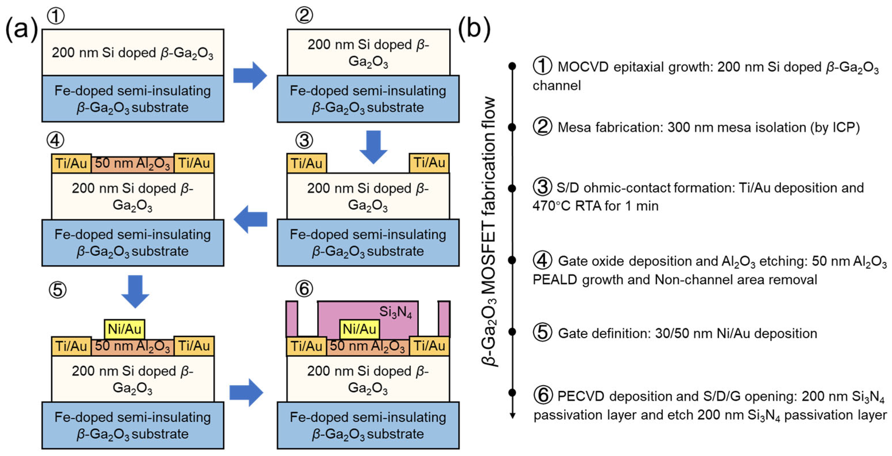
This study employed metal–organic chemical vapor deposition (MOCVD) using trimethyl-gallium and high-purity oxygen as precursors to epitaxially grow a 200 nm thick β-Ga2O3 film on a lightly doped, semi-insulating single crystal Ga2O3 substrate (010). Figure 1a,b shows the cross-sectional views of lateral β-Ga2O3 MOSFET devices without and with a silicon nitride layer, respectively, along with their corresponding top-view optical microscope images (Figure 1c,d). Figure 2 illustrates the fabrication process of the β-Ga2O3 MOSFET. First, 200 nm Si-doped β-Ga2O3 channel layers were epitaxially grown on Fe-doped semi-insulating (010) β-Ga2O3 substrates via MOCVD. Device isolation was achieved by inductively coupled plasma (ICP) dry etching to form 300 nm mesas. Source (S) and Drain (D) electrode regions were defined by photolithography and Ti/Au (30/50 nm) electrodes were deposited by electron beam evaporation and patterned via lift-off. A 50 nm Al2O3 gate oxide was then deposited via plasma-enhanced atomic layer deposition (PEALD). Gate electrodes (Ni/Au = 30/50 nm) were deposited by magnetron sputtering. Finally, a 200 nm Si3N4 passivation layer was grown via Plasma Enhancd Chemical Vapor Deposition (PECVD), with S/D and gate openings etched to complete device fabrication. The channel length (LSD) was set to 40/30/20 μm, the gate length (LG) to 8 μm, and the gate side region length (LGS) and gate bottom region length (LGD) to 8 μm and 28/18/8 μm, respectively. The asymmetric structure of LGS and LGD was intentionally designed to enhance the MOSFET’s tolerance for higher breakdown voltages.

3. Results

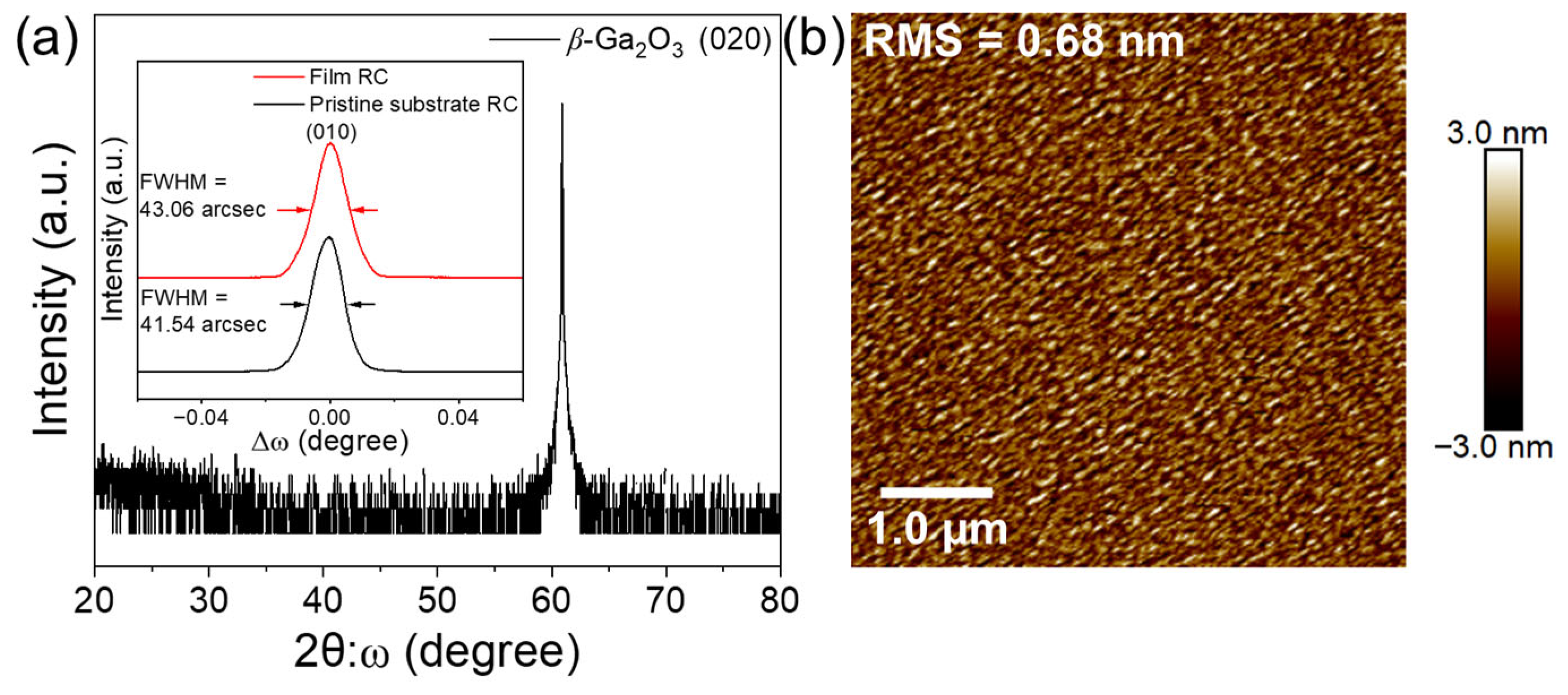
As demonstrated in Figure 3a, XRD analysis confirms the epitaxial growth and ultrahigh growth quality of the β-Ga2O3 epitaxial film. The rocking curve of the β-Ga2O3 epitaxial film shows a narrow Full Width at Half Maximum (FWHM) value of 43.06 arcsec for the (020) reflection, which is very close to the FWHM value of 41.54 arcsec measured for the pristine single-crystal substrate, indicating excellent crystalline quality comparable to that of the single-crystal substrate [24]. As shown in Figure 3b, AFM characterization reveals a smooth surface with an RMS roughness of only 0.68 nm, which is beneficial for the device fabrication as it minimizes interface scattering and promotes the formation of high-quality gate–channel interfaces [25,26]. Furthermore, Hall-effect measurements yield a carrier concentration of 5.13 × 1017 cm−3 and a mobility of 96.2 cm2·V−1·s−1, underscoring the excellent electrical transport properties of the epitaxial layer.
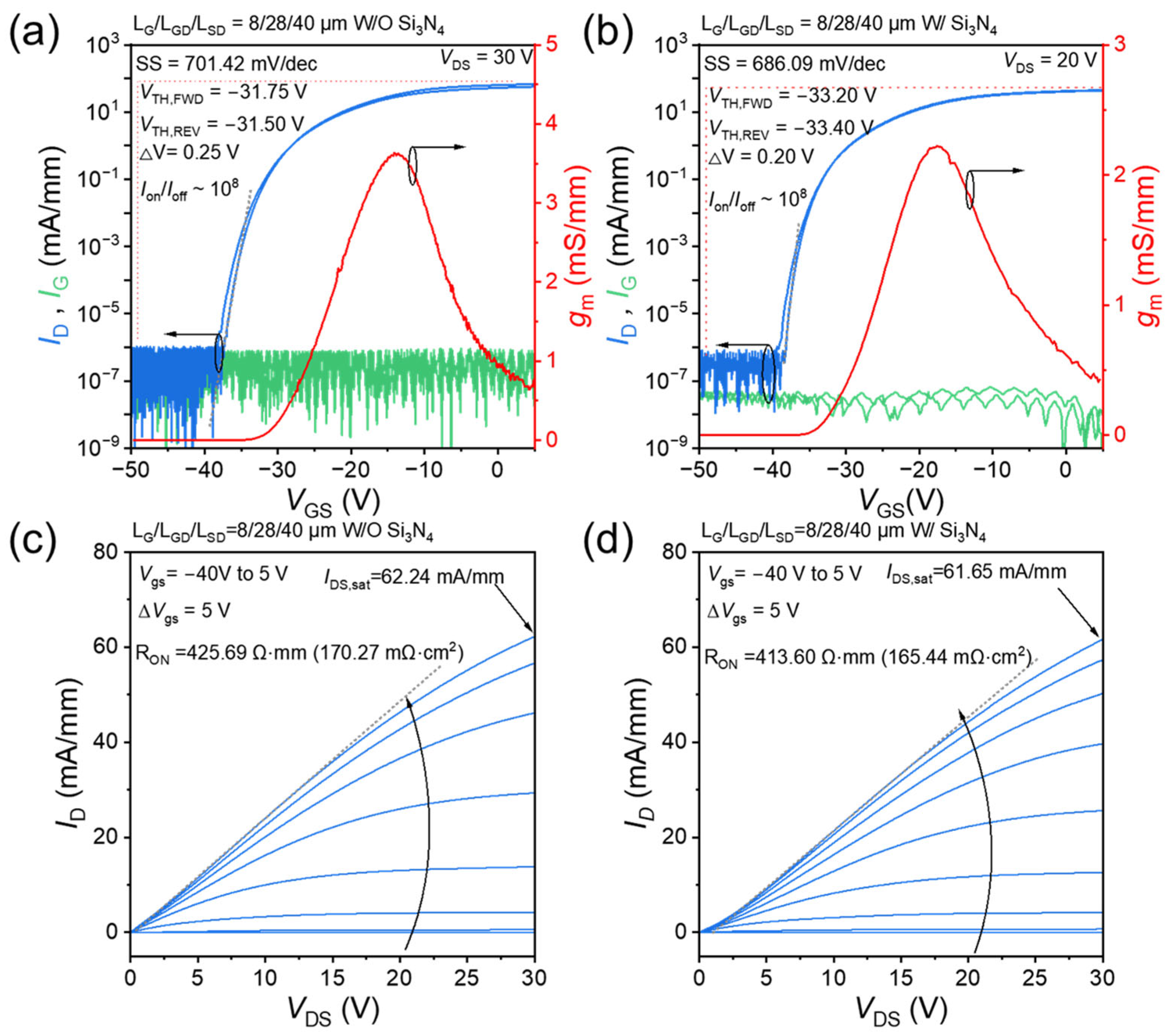
Using Keysight B1500A semiconductor characterization system, DC I-V measurement of β-Ga2O3 MOSFETs (with LG = 8 μm and LGD = 28 μm) was carried out at room temperature. Figure 4a,b shows the measured transfer characteristics of the MOSFETs without a Si3N4 terminal structure (denoted as W/O Si3N4 device) and that with a Si3N4 terminal structure (W/Si3N4 device) at a constant VDS = 30 V and VDS = 20 V, respectively. Figure 4a shows the log-scale transfer curve of W/O Si3N4 MOSFET. Threshold voltage (Vth), defined as the voltage at which ID = 0.1 mA·mm−1, was extracted to be −31.75 V from the forward curve. There exists small sweep hysteresis (ΔV = 0.25 V) in the forward and reverse VGS sweep. Such negligible hysteresis implies the high-quality interface for the devices [27]. A maximum transconductance (gm, max) and sub-threshold swing (SS) of 3.63 mS/mm and 701.42 mV/dec were extracted respectively. Figure 4b shows the log-scale transfer curve of W/Si3N4 MOSFET. The Vth was extracted to be −33.20 V from the forward curve. A maximum transconductance and sub-threshold swing (SS) of 2.22 mS/mm and 686.09 mV/dec were extracted respectively. There exists small sweep hysteresis (ΔV = 0.20 V) in the forward and reverse VGS sweep. The on/off ratios of W/O Si3N4 device and W Si3N4 device were extracted to be 108. Both devices exhibit excellent off-state characteristics at Vgs = −40 V, with a negligible leakage current of 10−7 mA/mm. The low gate and source–drain leakage indicated minimal surface and bulk-related leakage in these devices. Figure 4c,d shows DC output family curves of W/O Si3N4 device and W/Si3N4 device from Vgs = −40 V to Vgs = +5 V with a gate voltage step of 5 V. As shown in Figure 4c, W/O Si3N4 device achieved a saturation drain–current density (ID, sat) of 62.24 mA/mm at Vgs = 5 V and VDS = 10 V. The on-resistance (RON) is 425.69 Ω·mm when normalized to the channel width (Wc), and the specific on-resistance (Ron, sp) is 170.27 mΩ·cm2 when normalized to the channel area Wc × LSD. As shown in Figure 4d, W/Si3N4 device achieved ID, sat = 61.65 mA/mm at Vgs = 5 V and VDS = 10 V. The RON is 413.60 Ω·mm when normalized to the Wc, and the Ron, sp is 165.44 mΩ·cm2 when normalized to the channel area Wc × LSD. The nearly identical electrical performance demonstrates that the Si3N4 terminal structure does not compromise the on-state device performance. Additionally, similar electrical characteristics are observed for devices with LGD = 8 and 18 μm (as detailed in Supporting Information Figures S1 and S2), demonstrating that the Si3N4 layer adds very few interface states. These results suggest that the inclusion of the Si3N4 layer exerts little impact on the device’s forward conduction behavior [28].
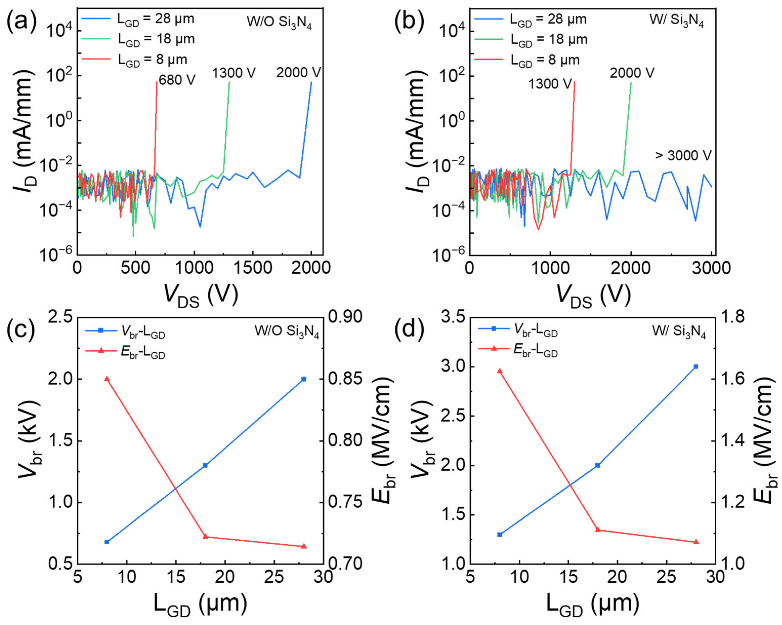
Three-terminal breakdown measurements were performed in Fluorinert FC-40 to avoid air breakdown. Figure 5a shows the breakdown characteristics of W/O Si3N4 device at Vgs = −40 V for different gate–drain distances (LGD). The breakdown voltage (Vbr) increases with LGD, reaching 680 V, 1300 V, and 2000 V for LGD = 8 μm, 18 μm, and 28 μm, respectively. In contrast, as shown in Figure 5b, the W/Si3N4 device delivers substantially higher Vbr values of 1300 V, 2000 V, and >3000 V for the same LGD conditions. Figure 5c,d summarize the dependences of Vbr and Ebr on LGD for the W/O Si3N4 and W/Si3N4 devices, respectively. For W/O Si3N4 device, Vbr increases with LGD, while the average breakdown field (Ebr) decreases from 0.85 MV/cm at 8 μm to 0.71 MV/cm at 28 μm. Figure 5d presents the corresponding trends for W/Si3N4 device. Although Ebr still decreases with increasing LGD (from 1.63 MV/cm to 1.07 MV/cm), the W/Si3N4 device exhibits nearly twice the Ebr of W/O Si3N4 device at same LGD. This improvement demonstrates that the Si3N4 terminal structure can alleviate gate–drain electric field concentration, consequently boosting breakdown performance of the device [19,23,29,30].
Although the Si3N4 terminal structure effectively mitigates electric-field crowding, its thermal conductivity is only approximately 0.7 W/m·K [31], which is lower than that of β-Ga2O3, approximately 27 W/m·K [32]. Because the Si3N4 layer is located on the device surface and is relatively thin, its impact on the primary heat-flow path through the β-Ga2O3 epilayer/substrate is expected to be limited. Nevertheless, given the intrinsically low thermal conductivity of β-Ga2O3, thermal management remains critical for high-power operation and long-term device reliability. Future strategies such as substrate thinning, flip-chip bonding, integration with high-thermal-conductivity heat spreaders, and optimized backside heat extraction could help mitigate self-heating and improve device reliability.
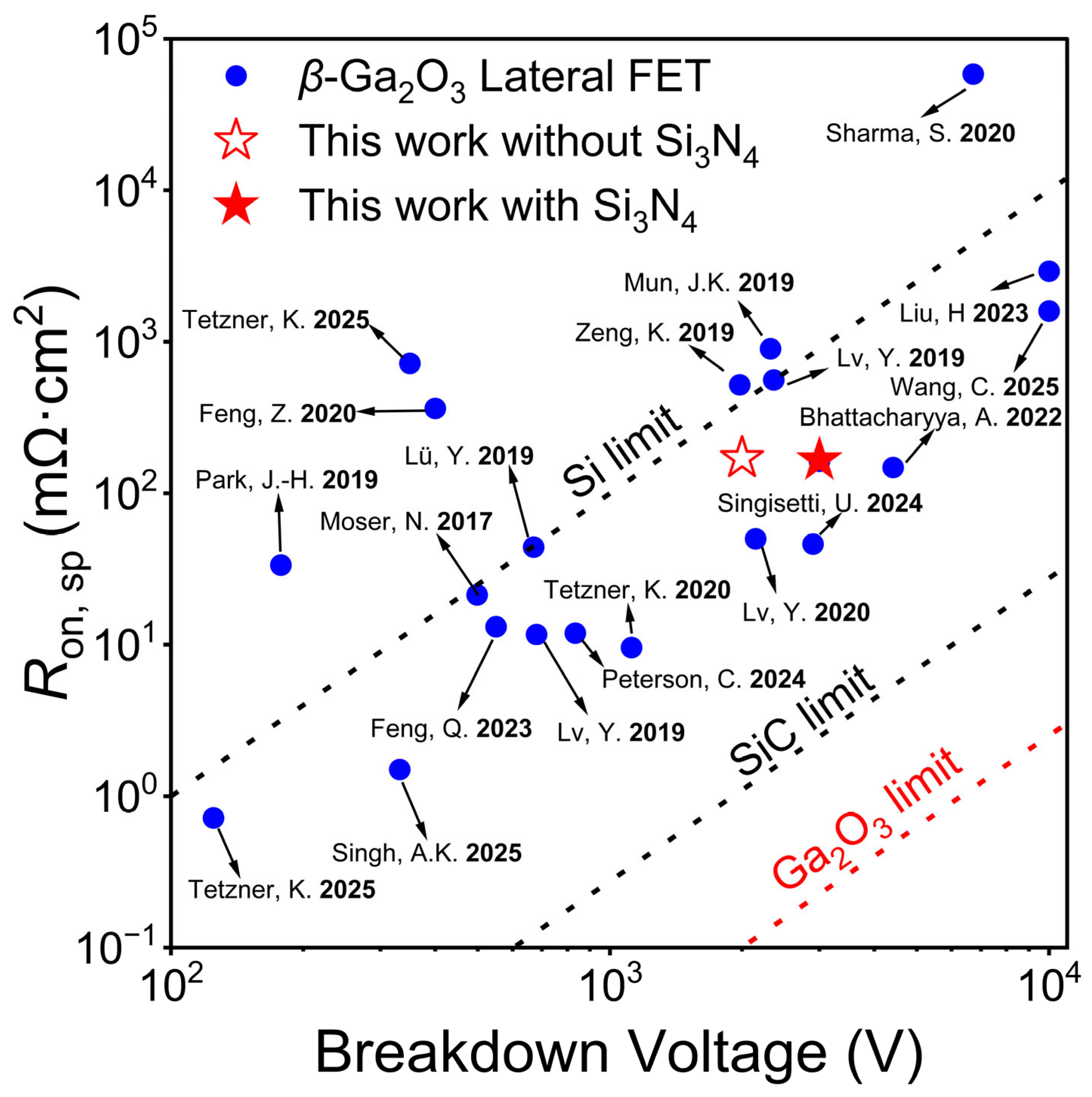
As illustrated in Figure 6, the specific on-resistance (Ron, sp) and breakdown voltage (Vbr) of advanced lateral β-Ga2O3 transistors are presented, with and without Si3N4 terminal structure. In comparison with other reported devices, this device demonstrates superior Vbr while typically offering more favorable Ron, sp. It can be inferred that the W/Si3N4 device (illustrated by a solid red star) attains an optimal equilibrium between Ron, Sp and Vbr, thereby situating its performance within the established theoretical limits of Si and SiC. This result provides substantial validation of the effectiveness of the Si3N4 terminal structure scheme. Experimental verification of the fabricated β-Ga2O3 MOSFETs in real power electronic systems is planned as part of our future work. Such studies will focus on assessing the device performance under practical operating conditions, including high-voltage switching behavior, dynamic reliability, and long-term stability.
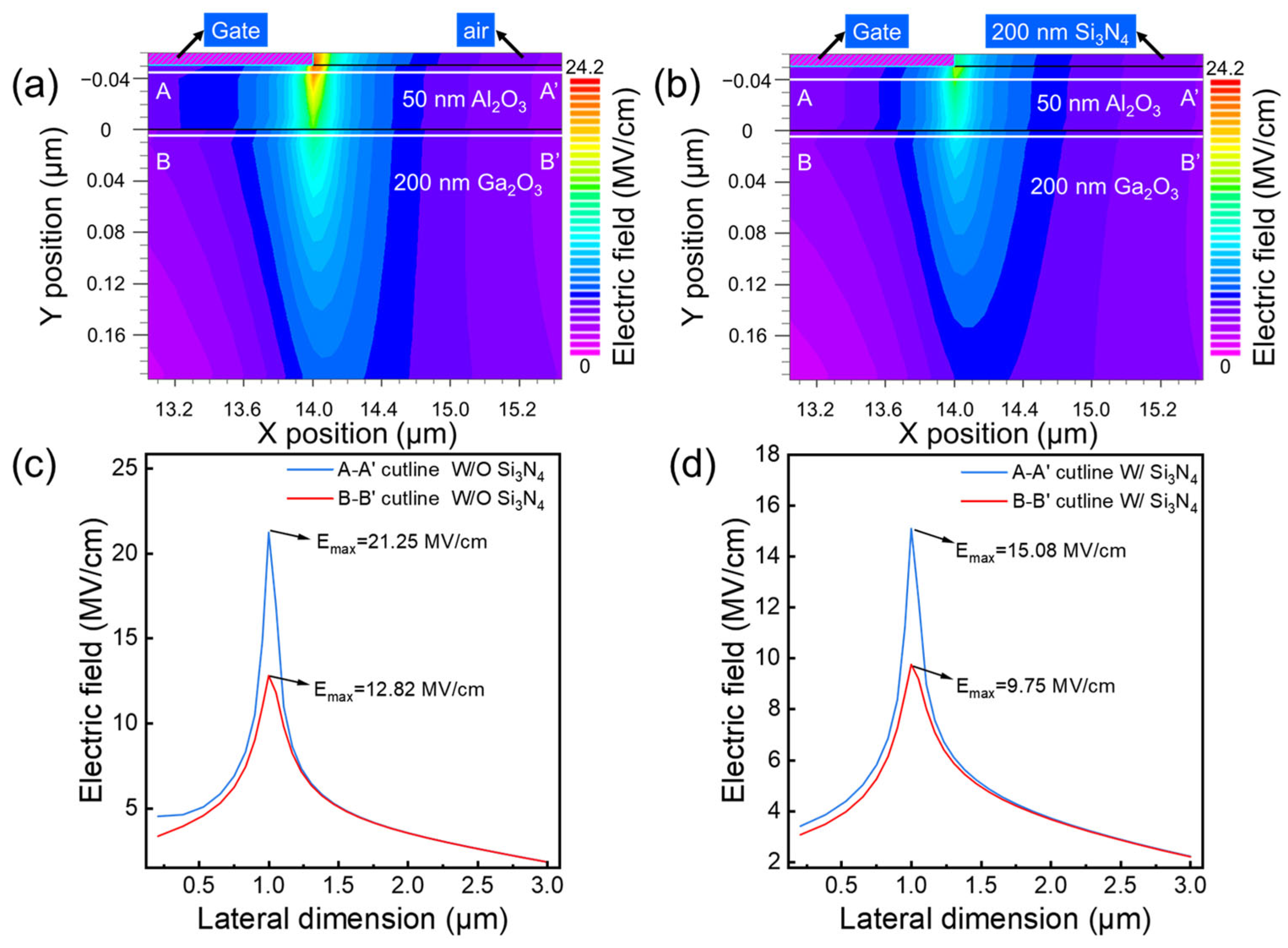
From ERETCAD-Env simulations, Figure 7 presents the simulated two-dimensional electric field distribution at the gate–drain edge of lateral β-Ga2O3 MOSFETs under a drain bias of 1000 V. Devices with and without a 200 nm Si3N4 terminal structure were compared, respectively. As illustrated in Figure 7a, in the absence of Si3N4, severe field crowding occurs at the gate–drain edge of the device, leading to pronounced electric field peaks in both the Al2O3 gate dielectric and the β-Ga2O3 epitaxial layer. In contrast, as shown in Figure 7b incorporation of the Si3N4 terminal structure significantly homogenizes the electric field distribution, effectively mitigating electric field crowding [11,35,44]. The peak electric fields at the dielectric/epitaxial interface are quantitatively compared in Figure 7c,d. Figure 7c shows that without Si3N4, the peak fields in the β-Ga2O3 epitaxial layer and the Al2O3 gate dielectric reach 12.82 MV/cm and 21.25 MV/cm, respectively. Figure 7d displays that with the Si3N4 layer, these peaks decrease to 9.75 MV/cm and 15.08 MV/cm, respectively, which attributed to the more uniform dispersion of the electric field from the gate edge toward the drain. Consequently, the breakdown voltage increases from 2000 V to over 3000 V. Additionally, for devices with LGD = 18 μm, the simulation results exhibit a trend consistent with that of devices with LGD = 28 μm (as detailed in Supporting Information Figure S3). These results strongly demonstrate that the Si3N4 terminal structure effectively alleviates electric field crowding, thereby substantially enhancing the breakdown voltage of β-Ga2O3 MOSFETs.

4. Conclusions

We demonstrate a lateral β-Ga2O3 MOSFET with a Si3N4 terminal structure that achieves a breakdown voltage surpassing 3 kV. After the introduction of the Si3N4 terminal structure, the device does not compromise the on-state device performance, with Vth = −31.75 V, SS = 701.42 mV/dec, ID, sat = 61.65 mA/mm and Ron, sp = 165.44 mΩ·cm2. For LGD = 8, 18, and 28 μm, the breakdown voltages increase from 680, 1300, and 2000 V to 1300, 2000, and over 3000 V, respectively. The average breakdown field is enhanced from 0.85 to 1.63 MV/cm. Electric field simulations confirm that this improvement originates from the mitigation of electric field crowding at the gate edge by the Si3N4 terminal structure. Collectively, these results demonstrate that the Si3N4 terminal design provides a simple and effective approach to improving the high-voltage performance of lateral β-Ga2O3 MOSFETs. Future work will focus on thermal optimization, dynamic reliability evaluation, and experimental verification in practical power electronic systems.

Supplementary Materials

The following supporting information can be downloaded at https://www.mdpi.com/article/10.3390/electronics15112337/s1: Figure S1: (a) Transfer and (c) output transfer curves for the β-Ga2O3 MOSFET without Si3N4 terminal structure. (b) Transfer and (d) output transfer curves for the MOSFET with Si3N4 terminal structure. (LSD = 30 μm); Figure S2. (a) Transfer and (c) transfer curves for the β-Ga2O3 MOSFET without Si3N4 terminal structure. (b) Transfer and (d) output transfer curves for the MOSFET with Si3N4 terminal structure. (LSD = 20 μm); Figure S3. Simulation of electric field distribution for LGD = 18 μm MOSFETs at a drain bias of 800 V: (a) without Si3N4 terminal structure, (b) with Si3N4 terminal structure. (c) Electric field distributions along cutlines A-A’ and B-B’ extracted from (a). (d) Electric field distributions along cutlines A-A’ and B-B’ extracted from (b).

Author Contributions

Conceptualization and funding acquisition, N.L., W.Z.; data curation and writing—original draft preparation, H.Z.; software, Z.W. and X.L.; investigation, Z.Y., C.L. and S.Z.; resources, W.Y.; writing—review and editing, N.L., J.Y. and W.Z. All authors have read and agreed to the published version of the manuscript.

Funding

This research was funded by the National Natural Science Foundation of China, grant number 62204244 and the Zhejiang Provincial Natural Science Foundation of China, grant number LQ23F040003 and the Ningbo Yongjiang Talent Introduction Programme, grant number 2021A-046-C.

Data Availability Statement

The data presented in this study are available within the article.

Conflicts of Interest

The authors declare no conflicts of interest.

Abbreviations

The following abbreviations are used in this manuscript:
RESURFReduced Surface Field
MOSFETMetal-Oxide-Semiconductor Field-Effect Transistor
MOCVDMetal–Organic Chemical Vapor Deposition
ICPInductively Coupled Plasma
PEALDPlasma Enhanced Atomic Layer Deposition
PECVDPlasma Enhancd Chemical Vapor Deposition
XRDX-Ray Diffraction
FWHMFull Width at Half Maximum
AFMAtomic Force Microscope
RMSRoot Mean Square
W/OWithout
W/With
WcChannel Width

References

  1. Venkata Prasad, C.; Rim, Y.S. Review on interface engineering of low leakage current and on-resistance for high-efficiency Ga2O3-based power devices. Mater. Today Phys. 2022, 27, 100777. [Google Scholar] [CrossRef]
  2. Green, A.J.; Speck, J.; Xing, G.; Moens, P.; Allerstam, F.; Gumaelius, K.; Neyer, T.; Arias-Purdue, A.; Mehrotra, V.; Kuramata, A.; et al. β-Gallium oxide power electronics. APL Mater. 2022, 10, 029201. [Google Scholar] [CrossRef]
  3. Pearton, S.J.; Yang, J.; Cary, P.H.I.V.; Ren, F.; Kim, J.; Tadjer, M.J.; Mastro, M.A. A review of Ga2O3 materials, processing, and devices. Appl. Phys. Rev. 2018, 5, 011301. [Google Scholar] [CrossRef]
  4. Moser, N.; McCandless, J.; Crespo, A.; Leedy, K.; Green, A.; Neal, A.; Mou, S.; Ahmadi, E.; Speck, J.; Chabak, K.; et al. Ge-Doped β-Ga2O3 MOSFETs. IEEE Electron Device Lett. 2017, 38, 775–778. [Google Scholar] [CrossRef]
  5. Higashiwaki, M.; Sasaki, K.; Murakami, H.; Kumagai, Y.; Koukitu, A.; Kuramata, A.; Masui, T.; Yamakoshi, S. Recent progress in Ga2O3 power devices. Semicond. Sci. Technol. 2016, 31, 034001. [Google Scholar] [CrossRef]
  6. Higashiwaki, M.; Sasaki, K.; Kuramata, A.; Masui, T.; Yamakoshi, S. Development of gallium oxide power devices. Phys. Status Solidi (A) Appl. Mater. Sci. 2014, 211, 21–26. [Google Scholar] [CrossRef]
  7. Higashiwaki, M.; Murakami, H.; Kumagai, Y.; Kuramata, A. Current status of Ga2O3 power devices. Jpn. J. Appl. Phys. 2016, 55, 1202A1. [Google Scholar] [CrossRef]
  8. Zhang, M.; Liu, Z.; Yang, L.; Yao, J.; Chen, J.; Zhang, J.; Wei, W.; Guo, Y.; Tang, W. β-Ga2O3-Based Power Devices: A Concise Review. Crystals 2022, 12, 406. [Google Scholar] [CrossRef]
  9. Yu, C.-h.; Guo, H.-m.; Liu, Y.; Wu, X.-D.; Zhang, L.-L.; Tan, X.; Han, Y.-C.; Ren, L. Simulation study on single-event burnout in field-plated Ga2O3 MOSFETs. Microelectron. Reliab. 2023, 149, 115227. [Google Scholar] [CrossRef]
  10. Tan, J.; Wei, J.; Li, X.; Wei, Y.; Dai, K.; Liu, R.; Li, Z.; Zhang, B.; Luo, X. Ultralow On-Resistance High-Voltage β-Ga2O3 MOSFET with an Extended p-NiO Gate Field Plate. IEEE Trans. Electron Devices 2026, 73, 138–144. [Google Scholar] [CrossRef]
  11. Lv, Y.; Zhou, X.; Long, S.; Song, X.; Wang, Y.; Liang, S.; He, Z.; Han, T.; Tan, X.; Feng, Z.; et al. Source-Field-Plated β-Ga2O3 MOSFET with Record Power Figure of Merit of 50.4 MW/cm2. IEEE Electron Device Lett. 2019, 40, 83–86. [Google Scholar] [CrossRef]
  12. Alam, M.Z.; Khan, I.A.; Amin, S.I.; Anam, A. β-Ga2O3 trench-gate MOSFET with VLD and field plate design for enhanced RF, thermal, breakdown voltage, and switching application. Phys. Scr. 2026, 101, 015004. [Google Scholar] [CrossRef]
  13. Higashiwaki, M. Gallium Oxide Power Electronics: The Key Semiconductor for Realizing Energy Sustainable Future. IEEE Electron Devices Mag. 2024, 2, 42-C3. [Google Scholar] [CrossRef]
  14. Zeng, K.; Vaidya, A.; Singisetti, U. A field-plated Ga2O3 MOSFET with near 2-kV breakdown voltage and 520 mΩ·cm2 on-resistance. Appl. Phys. Express 2019, 12, 081003. [Google Scholar] [CrossRef]
  15. Mun, J.K.; Cho, K.; Chang, W.; Jung, H.-W.; Do, J. Editors’ Choice—2.32 kV Breakdown Voltage Lateral β-Ga2O3 MOSFETs with Source-Connected Field Plate. ECS J. Solid State Sci. Technol. 2019, 8, Q3079. [Google Scholar] [CrossRef]
  16. Qu, Y.; Ren, B.; Yuan, J.; Deng, N.; Hu, W.; Liu, H.; Yuan, Y.; Wu, S.; Wang, H. Enhanced thermal stability of Ga2O3 MOSFETs with nanocrystalline diamond field plate. Diam. Relat. Mater. 2023, 133, 109753. [Google Scholar] [CrossRef]
  17. Chen, J.; Zhang, X.; Zhao, J.; Wei, J.; Hua, M. RESURF Ga2O3-on-SiC Field Effect Transistors for Enhanced Breakdown Voltage. IEEE J. Electron Devices Soc. 2025, 13, 570–576. [Google Scholar] [CrossRef]
  18. Acharjee, N.; Singh, S.; Dadi, A.P.; Bordoloi, S.; Ray, A. Investigation of High-k Dielectric Passivation Effects on DC Performance of AlN/β-Ga2O3 HEMTs. Semiconductors 2025, 59, 452–464. [Google Scholar] [CrossRef]
  19. Lv, Y.; Zhou, X.; Long, S.; Liang, S.; Song, X.; Zhou, X.; Dong, H.; Wang, Y.; Feng, Z.; Cai, S. Lateral source field-plated β-Ga2O3 MOSFET with recorded breakdown voltage of 2360 V and low specific on-resistance of 560 mΩ·cm2. Semicond. Sci. Technol. 2019, 34, 11LT02. [Google Scholar] [CrossRef]
  20. Goyal, P.; Kaur, H. Exploring the efficacy of implementing field plate design with air gap on β-Ga2O3 MOSFET for high power & RF applications. Micro Nanostruct. 2023, 173, 207454. [Google Scholar] [CrossRef]
  21. Tetzner, K.; Hilt, O.; Popp, A.; Bin Anooz, S.; Würfl, J. Challenges to overcome breakdown limitations in lateral β-Ga2O3 MOSFET devices. Microelectron. Reliab. 2020, 114, 113951. [Google Scholar] [CrossRef]
  22. Taboada Vasquez, J.M.; Li, X. A Review of Vertical Ga2O3 Diodes: From Fabrication to Performance Optimization and Future Outlooks. Phys. Status Solidi (B) 2025, 262, 2400635. [Google Scholar] [CrossRef]
  23. Sharma, S.; Zeng, K.; Saha, S.; Singisetti, U. Field-Plated Lateral Ga2O3 MOSFETs with Polymer Passivation and 8.03 kV Breakdown Voltage. IEEE Electron Device Lett. 2020, 41, 836–839. [Google Scholar] [CrossRef]
  24. Li, Z.; Jiao, T.; Yu, J.; Hu, D.; Lv, Y.; Li, W.; Dong, X.; Zhang, B.; Zhang, Y.; Feng, Z.; et al. Single crystalline β-Ga2O3 homoepitaxial films grown by MOCVD. Vacuum 2020, 178, 109440. [Google Scholar] [CrossRef]
  25. Madadi, D.; Orouji, A.A. Scattering mechanisms in β-Ga2O3 junctionless SOI MOSFET: Investigation of electron mobility and short channel effects. Mater. Today Commun. 2021, 26, 102044. [Google Scholar] [CrossRef]
  26. Wang, X.-C.; Lu, X.-L.; He, Y.-L.; Zhang, F.; Shao, Y.; Liu, P.; Zhang, Z.-N.; Zheng, X.-F.; Chen, W.-W.; Wang, L.; et al. Quasi-2D high mobility channel E-mode β-Ga2O3 MOSFET with Johnson FOM of 7.56 THz·V. Appl. Phys. Lett. 2024, 125, 063505. [Google Scholar] [CrossRef]
  27. Wang, C.; Zhou, H.; Zhang, J.; Mu, W.; Wei, J.; Jia, Z.; Zheng, X.; Luo, X.; Tao, X.; Hao, Y. Hysteresis-free and μs-switching of D/E-modes Ga2O3 hetero-junction FETs with the BV2/Ron, sp of 0.74/0.28 GW/cm2. Appl. Phys. Lett. 2022, 120, 112101. [Google Scholar] [CrossRef]
  28. Joishi, C.; Zhang, Y.; Xia, Z.; Sun, W.; Arehart, A.R.; Ringel, S.; Lodha, S.; Rajan, S. Breakdown Characteristics of β-(Al0.22Ga0.78)2O3/Ga2O3 Field-Plated Modulation-Doped Field-Effect Transistors. IEEE Electron Device Lett. 2019, 40, 1241–1244. [Google Scholar] [CrossRef]
  29. Lv, Y.; Zhou, X.; Long, S.; Wang, Y.; Song, X.; Zhou, X.; Xu, G.; Liang, S.; Feng, Z.; Cai, S.; et al. Enhancement-Mode β-Ga2O3 Metal-Oxide-Semiconductor Field-Effect Transistor with High Breakdown Voltage over 3000 V Realized by Oxygen Annealing. Phys. Status Solidi (RRL)—Rapid Res. Lett. 2020, 14, 1900586. [Google Scholar] [CrossRef]
  30. Tetzner, K.; Treidel, E.B.; Hilt, O.; Popp, A.; Anooz, S.B.; Wagner, G.; Thies, A.; Ickert, K.; Gargouri, H.; Würfl, J. Lateral 1.8 kV β-Ga2O3 MOSFET with 155 MW/cm2 Power Figure of Merit. IEEE Electron Device Lett. 2019, 40, 1503–1506. [Google Scholar] [CrossRef]
  31. Hadi, M.; Pailhès, S.; Debord, R.; Benamrouche, A.; Drouard, E.; Gehin, T.; Botella, C.; Leclercq, J.L.; Noe, P.; Fillot, F.; et al. Transient thermal conductivity in PECVD SiNx at high temperature: The thermal signature of an on-going irreversible modification. Materialia 2022, 26, 101574. [Google Scholar] [CrossRef]
  32. Sasaki, K. Prospects for β-Ga2O3: Now and into the future. Appl. Phys. Express 2024, 17, 090101. [Google Scholar] [CrossRef]
  33. Tetzner, K.; Halhoul, H.; Cuallo, M.D.; Hilt, O. 4 A/300 V Switching of Lateral β-Ga2O3 MOSFET Devices. IEEE Electron Device Lett. 2025, 46, 1601–1604. [Google Scholar] [CrossRef]
  34. Wang, C.; Sun, S.; Su, C.; Zhou, H.; Zhang, J.; Hao, Y. Breakdown voltage over 10 kV β-Ga2O3 heterojunction FETs with RESURF structure. Sci. China Inf. Sci. 2025, 68, 169401. [Google Scholar] [CrossRef]
  35. Bhattacharyya, A.; Sharma, S.; Alema, F.; Ranga, P.; Roy, S.; Peterson, C.; Seryogin, G.; Osinsky, A.; Singisetti, U.; Krishnamoorthy, S. 4.4 kV β-Ga2O3 MESFETs with power figure of merit exceeding 100 MW·cm−2. Appl. Phys. Express 2022, 15, 061001. [Google Scholar] [CrossRef]
  36. Saha, C.N.; Vaidya, A.; Nipu, N.J.; Meng, L.; Yu, D.S.; Zhao, H.; Singisetti, U. Thin channel Ga2O3 MOSFET with 55 GHz fMAX and >100 V breakdown. Appl. Phys. Lett. 2024, 125, 062101. [Google Scholar] [CrossRef]
  37. Tetzner, K.; Thies, A.; Brusaterra, E.; Külberg, A.; Paul, P.; Ostermay, I.; Würfl, J.; Hilt, O. All-implanted lateral β-Ga2O3 MOSFET devices realized on semi-insulating (-201) β-Ga2O3 substrates. Appl. Phys. Lett. 2025, 126, 062105. [Google Scholar] [CrossRef]
  38. Singh, A.K.; Huang, S.; Shen, J.-H.; Wu, T.-H.; Lee, W.-H.; Yen, C.-C.; Chou, H.-Y.; Chiang, W.-H.; Huang, C.-Y.; Liu, P.-L.; et al. Performance Enhancement of MOCVD Grown β-Ga2O3 MOSFETs on Silicon Substrates via AlN Buffer Layer. ACS Appl. Electron. Mater. 2025, 7, 512–519. [Google Scholar] [CrossRef]
  39. Park, J.-H.; McClintock, R.; Jaud, A.; Dehzangi, A.; Razeghi, M. MOCVD grown β-Ga2O3 metal-oxide-semiconductor field effect transistors on sapphire. Appl. Phys. Express 2019, 12, 095503. [Google Scholar] [CrossRef]
  40. Feng, Z.; Tian, X.; Li, Z.; Hu, Z.; Zhang, Y.; Kang, X.; Ning, J.; Zhang, Y.; Zhang, C.; Feng, Q.; et al. Normally-Off-β-Ga2O3 Power MOSFET with Ferroelectric Charge Storage Gate Stack Structure. IEEE Electron Device Lett. 2020, 41, 333–336. [Google Scholar] [CrossRef]
  41. Lü, Y.; Song, X.; He, Z.; Wang, Y.; Tan, X.; Liang, S.; Wei, C.; Zhou, X.; Feng, Z. Source-field-plated Ga2O3 MOSFET with a breakdown voltage of 550 V. J. Semicond. 2019, 40, 012803. [Google Scholar] [CrossRef]
  42. Cai, Y.; Feng, Z.; Wang, Z.; Song, X.; Hu, Z.; Tian, X.; Zhang, C.; Liu, Z.; Feng, Q.; Zhou, H.; et al. Demonstration of the normally off β-Ga2O3 MOSFET with high threshold voltage and high current density. Appl. Phys. Lett. 2023, 123, 193501. [Google Scholar] [CrossRef]
  43. Peterson, C.; Alema, F.; Bhattacharyya, A.; Ling, Z.; Roy, S.; Osinsky, A.; Krishnamoorthy, S. Kilovolt-class β-Ga2O3 MOSFETs on 1-in. bulk substrates. Appl. Phys. Lett. 2024, 124, 082104. [Google Scholar] [CrossRef]
  44. Lv, Y.; Liu, H.; Zhou, X.; Wang, Y.; Song, X.; Cai, Y.; Yan, Q.; Wang, C.; Liang, S.; Zhang, J.; et al. Lateral β-Ga2O3 MOSFETs with High Power Figure of Merit of 277 MW/cm2. IEEE Electron Device Lett. 2020, 41, 537–540. [Google Scholar] [CrossRef]
  45. Liu, H.; Wang, Y.; Lv, Y.; Han, S.; Han, T.; Dun, S.; Guo, H.; Bu, A.; Feng, Z. 10-kV Lateral β-Ga2O3 MESFETs with B Ion Implanted Planar Isolation. IEEE Electron Device Lett. 2023, 44, 1048–1051. [Google Scholar] [CrossRef]
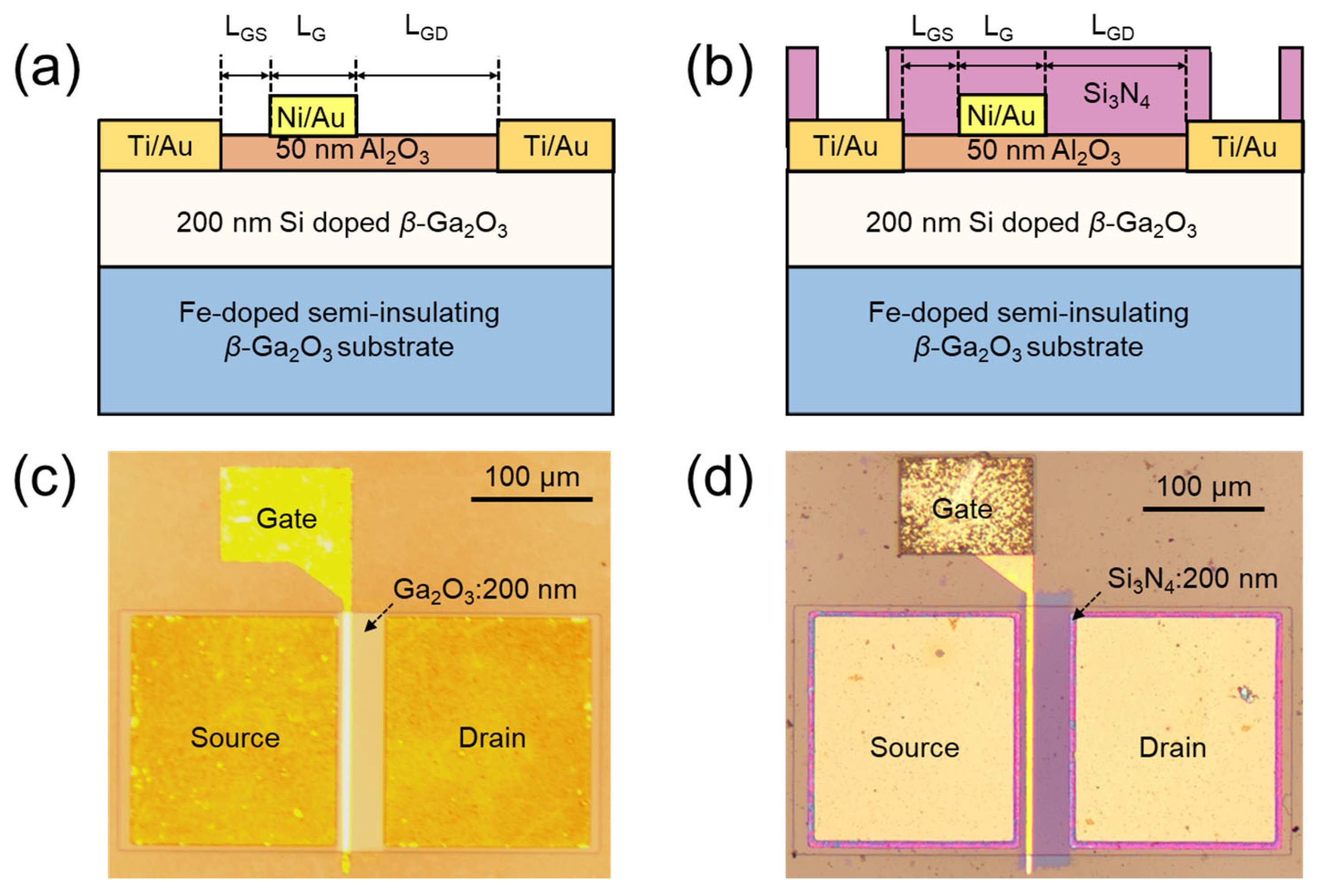
Figure 1. Schematic of the cross-section structure of lateral β-Ga2O3 MOSFETs (a) without and (b) with Si3N4 terminal structure. Top-view optical microscope images of the MOSFETs (c) without Si3N4 and (d) with Si3N4. The structure parameters include LGS/LG = 4 μm/8 μm and the Si3N4 layer thickness = 200 nm.
Electronics 15 02337 g001
Figure 2. Fabrication process of the β-Ga2O3 MOSFET (a) Schematic of the cross-sectional device structure during each process step. (b) Fabrication process of the β-Ga2O3 MOSFET with a Si3N4 terminal structure.
Electronics 15 02337 g002
Figure 3. Structural and morphological characterization of the Si-doped β-Ga2O3 epitaxial film on a (010) β-Ga2O3 substrate. (a) 2θ:ω XRD pattern and (a-inset) rocking curve of the Si doped β-Ga2O3 film deposited on a (010) β-Ga2O3 substrate. (b) AFM image of the β-Ga2O3 epitaxial film.
Electronics 15 02337 g003
Figure 4. Characteristic I-V curves of β-Ga2O3 MOSFETs. Transfer curves for the β-Ga2O3 MOSFET (a) without Si3N4 terminal structure and (b) with Si3N4 terminal structure. Output curves for the β-Ga2O3 MOSFET (c) without Si3N4 terminal structure and (d) with Si3N4 terminal structure.
Electronics 15 02337 g004
Figure 5. (a) Breakdown curves for the MOSFET without Si3N4 terminal structure, with LGD = 8/18/28 μm. (b) Breakdown curves for the MOSFET with Si3N4 terminal structure, with LGD = 8/18/28 μm. (c) Relationship between breakdown voltage (Vbr)/average breakdown field strength (Ebr) and LGD for the MOSFET without Si3N4 terminal structure. (d) Relationship between Vbr/Ebr and LGD for the MOSFET with Si3N4 terminal structure.
Electronics 15 02337 g005
Figure 6. Plot of the Ron, sp vs. Vbr for benchmarking of the MOSFETs performance of this work with other recently published data of lateral β-Ga2O3 power transistor devices [4,11,14,15,19,21,23,33,34,35,36,37,38,39,40,41,42,43,44,45].
Electronics 15 02337 g006
Figure 7. Simulation of electric field distribution for LGD = 28 μm MOSFETs at a drain bias of 1000 V using ERETCAD-Env: (a) without Si3N4 terminal structure. (b) with Si3N4 terminal structure. (c) Electric field distributions along cutlines A-A’ and B-B’ extracted from (a). (d) Electric field distributions along cutlines A-A’ and B-B’ extracted from (b).
Electronics 15 02337 g007
Disclaimer/Publisher’s Note: The statements, opinions and data contained in all publications are solely those of the individual author(s) and contributor(s) and not of MDPI and/or the editor(s). MDPI and/or the editor(s) disclaim responsibility for any injury to people or property resulting from any ideas, methods, instructions or products referred to in the content.