Communication

Noise Optimization of VCO-ADCs Based on Ring Oscillators with Cascoded Inverter Delay Cells

Electronics Technology Department, Carlos III University, 28911 Madrid, Spain
*
Author to whom correspondence should be addressed.
Electronics 2026, 15(11), 2299; https://doi.org/10.3390/electronics15112299
Submission received: 27 April 2026 / Revised: 15 May 2026 / Accepted: 20 May 2026 / Published: 26 May 2026
(This article belongs to the Section Microelectronics)

Abstract

A key component of VCO-ADCs is the ring oscillator, which determines the circuit and quantization noise of the converter. The input-referred thermal and flicker noise of a VCO-ADC stems from the VCO driver source and the VCO phase noise. On the other hand, quantization noise depends on the oscillation frequency of the VCO with respect to the sampling frequency. An optimal VCO-ADC design should balance oscillation frequency with flicker and thermal contributions of the VCO. In this paper, we show a simple modification of the conventional stages used in VCO-ADC ring oscillators. The modification consists of including two extra transistors in series, isolating the inverter from the power rails when switching. This modification allows one to significantly increase the oscillation frequency while having similar phase noise contributions compared to other ring oscillator architectures with the same area and power.

1. Introduction

Most VCO-ADCs found in the literature [1,2] use a voltage-controlled oscillator (VCO) implemented with a ring oscillator (RO) using CMOS inverters. Ring oscillators are used because they allow the readout of multiple stages (phases) at the same time, allowing a finer quantization of the input signal for a given sampling frequency. As a consequence, quantization noise depends on the number of phases and the oscillation frequency of the RO [3]. This is in contrast with other VCO topologies, such as LC-tank [4] or relaxation oscillators [5,6], which output two phases that are 180° apart. Nevertheless, VCO-ADCs have other noise sources to be taken into account in the form of VCO phase noise. The phase noise efficiency of ROs falls between LC-tank oscillators and relaxation oscillators [7]. Nevertheless, ROs have several advantages with respect to LC-tank VCOs: Firstly, their tuning range can be driven from close to 0 Hz to two times their rest frequency, expanding their dynamic range. Secondly, their layout size is smaller than LC-tank implementations. And finally, they can be implemented easily in the MHz range with μW power consumption, making them ideal for sensor applications. The VCO phase noise includes noise coming from the driver circuit of the VCO, as well as the intrinsic noise of the oscillator itself. This phase noise is composed of flicker and thermal contributions, which are modulated by the oscillator frequency [8]. In a noise-optimized design for an RO, a tradeoff between oscillation frequency and flicker noise contributions is found. For a given current, increasing the size of each stage of the oscillator results in a decrease in the oscillation frequency. This limits the achievable noise floor for a given power, area, and sampling frequency. The analysis and optimization of the RO phase noise [9,10] is an active topic of research for further improving VCO-ADC performance.
In this paper, we propose a novel RO design that improves the oscillation frequency while keeping the same noise, power, and area as other known ring oscillators. To simplify the comparative analysis, we will focus on two commonly found RO topologies in the literature: the single-ended RO and the differential RO with feed-forward [11]. Both of these oscillators use conventional CMOS inverters with two MOS devices. In our design, we show a new delay cell that uses four MOS devices, implemented with the same total area as the stages of the compared RO architectures. The extra devices are in series with a two-transistor inverter and are driven by the internal nodes of the previous inverter stage. This implementation halves the capacitive load of every inverter stage while keeping the same noise and driving strength. As a consequence, the oscillation frequency is significantly increased while keeping the same input-referred noise. In this manuscript, we explain the design of the novel RO delay cell, we compare its performance against common RO topologies for the same implementation cost, and we review the performance of its physical implementation (layout) with respect to the schematic performance estimation. Additionally, we discuss why this novel RO can be an optimal solution for future VCO-ADC designs.

2. Materials and Methods

2.1. Ring Oscillators in VCO-ADCs

VCO-based ADCs came up as an alternative to oversampled converters suffering from downscaling and low voltage headroom, such as switched-capacitor circuits [12,13]. The ROs used in VCO-ADCs can be driven using simple analog stages with low gain given the high voltage-to-frequency sensitivity of the oscillator. This is the reason why many recent publications [14,15] provide almost all-digital architectures, which are more suited for cutting-edge CMOS nodes. Furthermore, VCO-ADCs can be configured in open-loop and closed-loop topologies. Closed-loop topologies [16,17] present SNDRs and FoMs similar to state-of-the-art ΣΔ modulators, while open-loop configurations [18,19] are well suited for amplifier-less sensor applications, achieving > 90 dBc of SFDR despite being considered a less linear counterpart.
A fundamental block of VCO-ADC architectures is the RO, translating the voltage input signal into a time-encoded signal, as illustrated in Figure 1. When no explicit feedback DAC is present, VCO-ADCs produce intrinsic first-order noise shaping [3]. Thus, the signal-to-quantization noise of the converter can be expressed as follows [3,20]:
S Q N R m a x [ d B ] = 6 · l o g 2 2 · λ · f e f f f s 3.41 + 9 · l o g 2 f s 2 · B W
In this equation, the first term 2 · λ · f e f f f s corresponds to the quantizer resolution: that is, the number of bits needed for the oscillator readout. As a result, the resolution depends on λ , being the number of counting edges (1 for either rising or falling edges and 2 for both); the effective frequency of the oscillator (which is the oscillation frequency times the number of stages in the oscillator, f e f f = N · f 0 ); and the sampling frequency ( f s ), which also determines the oversampling ratio. Note that, for a fixed current draw, increasing N does not affect f e f f , as f 0 decreases inversely proportional to N [11]. Thus, S Q N R is kept for a different number of phases in the RO.
Nevertheless, based on Equation (1), quantization noise benefits from running the oscillator at a higher frequency. In fact, doubling the oscillation frequency translates into one bit more on the quantizer and a 6 dB improvement on the S Q N R . Another possibility for improving the S Q N R is increasing the sampling frequency, which produces a 3 dB improvement. However, this is not always desirable because of the digital power increase, as well as the limits to the digital processing throughput.
Despite the improvement in quantization noise when increasing the oscillation frequency [3], increasing oscillation frequencies usually comes at a cost of either power or flicker noise [9,10,11]. Nevertheless, the main focus of this paper is on providing an RO topology comparison, as well as suggesting a new architecture that shows a higher oscillation frequency without affecting power consumption or noise efficiency.

2.2. Proposed RO Topology

ROs consist of an N number of stages that produce a delay proportional to the voltage applied, the current passing through them, and their size. In general, the delay stages are composed of inverters that are connected one after the other, forming a chain. The output of the last stage is fed back into the first to form a loop so that the circuit can oscillate. Depending on the application and the drive circuit, ROs can be controlled either by voltage or current.
Numerous topologies exist in the literature; however, the single-ended and feed-forward differential structures stand out for their high efficiency and low complexity. For this reason, they are selected in this study for evaluation with respect to the novel proposed architecture.
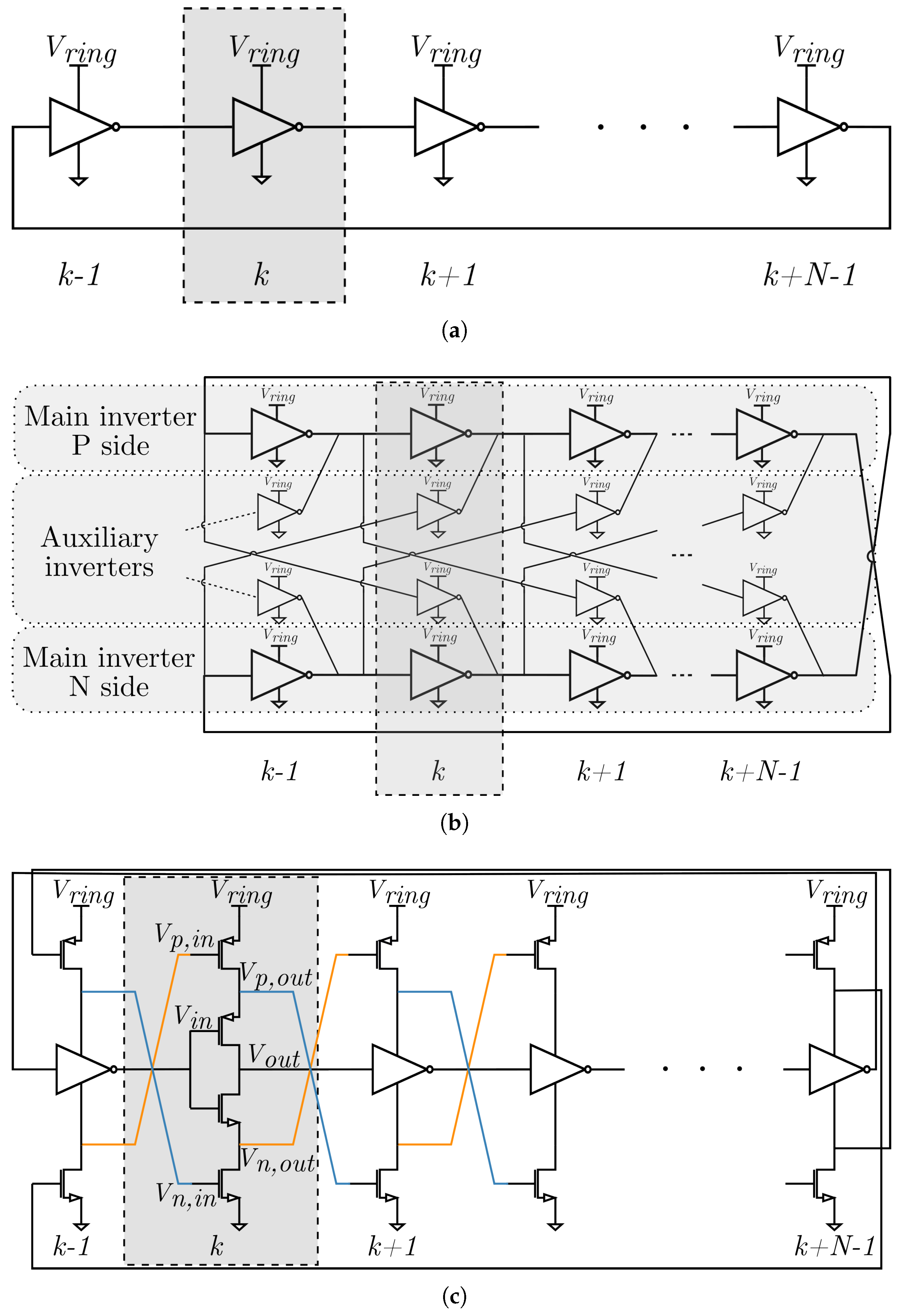
The single-ended topology is illustrated in Figure 2a. Its structure is made out of single CMOS inverters, formed by a PMOS device and an NMOS device. Notice that, in order for a RO to oscillate, it must satisfy the Barkhausen criteria. Thus, for a single-ended architecture, it is required to have an odd number of stages in the inverter chain.
On the other hand, differential ROs emerged as a solution to overcome, or at least mitigate, some limitations of the single-ended ROs. The differential property improves readout robustness and provides a better supply noise rejection interface. Differential ROs also bring other advantages, as they can provide negative feedback even with an even number of inverters in the chain. This optimizes the readout of the VCO-ADC, as it is possible to directly encode the phases of the RO into a binary number [21] when a 2 N stage number is used. In the literature, two differential topologies can be highlighted [11]: the direct cross-coupled and the feed-forward topologies; the latter is the focus of this study due to its improved performance. In both cases, each inverting cell consists of two parallel inverter paths that are 180 degrees apart (p and n sides) and synchronized by two auxiliary inverters. A circuit schematic is shown in Figure 2b. The main idea of this topology is that the auxiliary paths precharge the output of the main inverter paths. Looking at Figure 2b, the input of the k − 1 stage precharges the output of the k stage, allowing faster oscillation frequencies with the same power budget [22]. The criteria followed for the sizing of auxiliary inverters is to have equal strength as the main inverters (same size) to have optimum performance [11].

2.2.1. Cascode RO: Architecture Description

The proposed cascode RO topology is based on the single-ended RO. In this case, the ring oscillator consists of a chain of cascoded inverters, which are essentially a main inverter path formed by a PMOS and NMOS device, an outer PMOS, and NMOS transistors. As Figure 2c shows, the digital oscillating signal travels through the main inverter path, whereas the outer transistors are fed with the node voltage between NMOS devices of the k 1 cascode inverter cell in the case of the k PMOS device and between PMOS devices of the k 1 cell for the k NMOS device. Similarly to the single-ended topology, the non-differential inverter chain forces the condition that an odd number of inverters is required for oscillation.
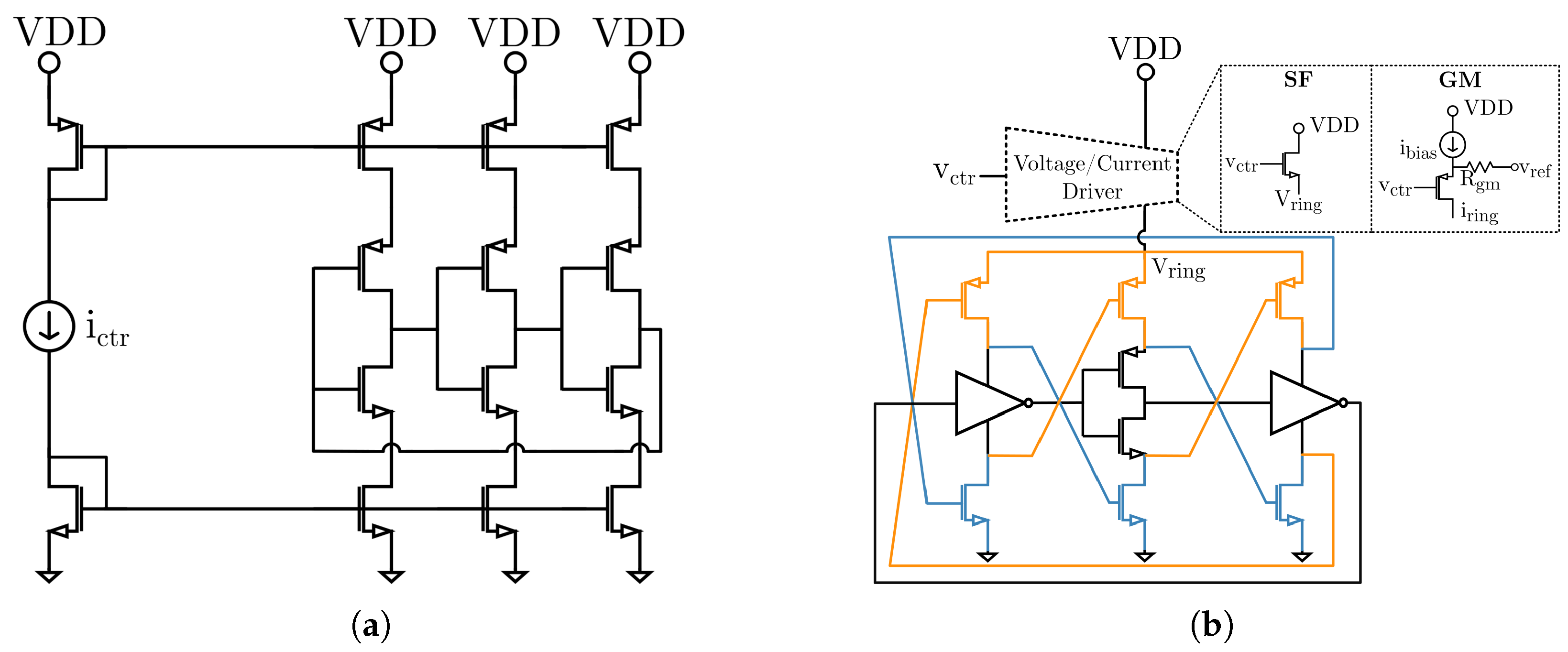
The proposed cascode RO structure resembles the common current-starved single-ended RO, as shown in Figure 3a. In this structure, each cell’s rise and fall times are controlled by a current mirror. Thus, the current being driven into the diodes of the current mirror controls the frequency of the ring oscillator. The sources of the current mirrors are typically referred to as VDD and VSS. In contrast, the proposed cascode ring oscillator is designed to be driven either by a current source (like a GM) or a voltage source (like an SF), which is not directly connected to VDD. This is shown in Figure 3b. The voltages controlling the cascode transistors are not generated by an external current mirror but self-generated and obtained from the previous phase of the RO. Structures with ROs being driven by SF or GM are commonly found for sensor readouts in the state of the art [23,24]. On the other hand, ROs driven by current mirrors are more common in the PLLs literature [25]. In fact, our novel cascode ring oscillator could also be driven by the current mirror structure of Figure 3a, resulting in a faster oscillation frequency in comparison with single-ended oscillators (for the same area and power).

2.2.2. Unit Cell Delay

To comprehend the working principle of this new topology, this paper will analyze the unit cell delay using the delay model used in [11]. The delay produced by a single-ended and cascode inverter can be obtained from the following expression:
0 τ d I r i n g C L = V M
where τ d represents the falling or rising edge delay of the inverter, and I r i n g represents the average current passing through the ring, which is assumed to be constant. In the case of V M , it represents the toggling point of the inverters, which is assumed to be approximately V r i n g 2 . Finally, C L is the load capacitance that accounts for all output capacitance, the input of the next inverter capacitance, and the readout buffer capacitance. This relationship leads to the final expression of the inverter delay [11]:
τ d = V r i n g · C L 2 · I r i n g
The period of oscillation is defined as the time needed for the rising and falling edge to propagate around the ring. Thus, in a ring formed by N inverters, the oscillation frequency could be expressed as the following:
f 0 = 1 N · ( τ d f + τ d r ) 1 N · 2 · τ d I r i n g N · C L · V r i n g
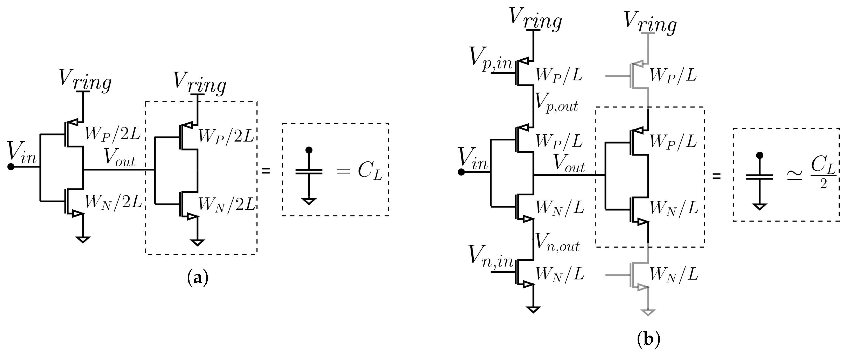
Therefore, based on this equation, for a constant I r i n g and V r i n g , the method of increasing oscillation frequencies is by reducing the load capacitance. In fact, having a look at the cascode RO cell in Figure 4b and comparing it with a single-ended RO cell with the same area, as shown in Figure 4a, the load capacitance is halved. Thus, it is expected that the oscillation frequency of the cascode cell increases close to double that of the single-ended cell. Note that, in this topology, V n , i n and V p , i n only suffer a small voltage variation at transition, and thus, the capacitive loading of these nodes to the previous inverter cell is minimal.

3. Results

3.1. Transient Simulations

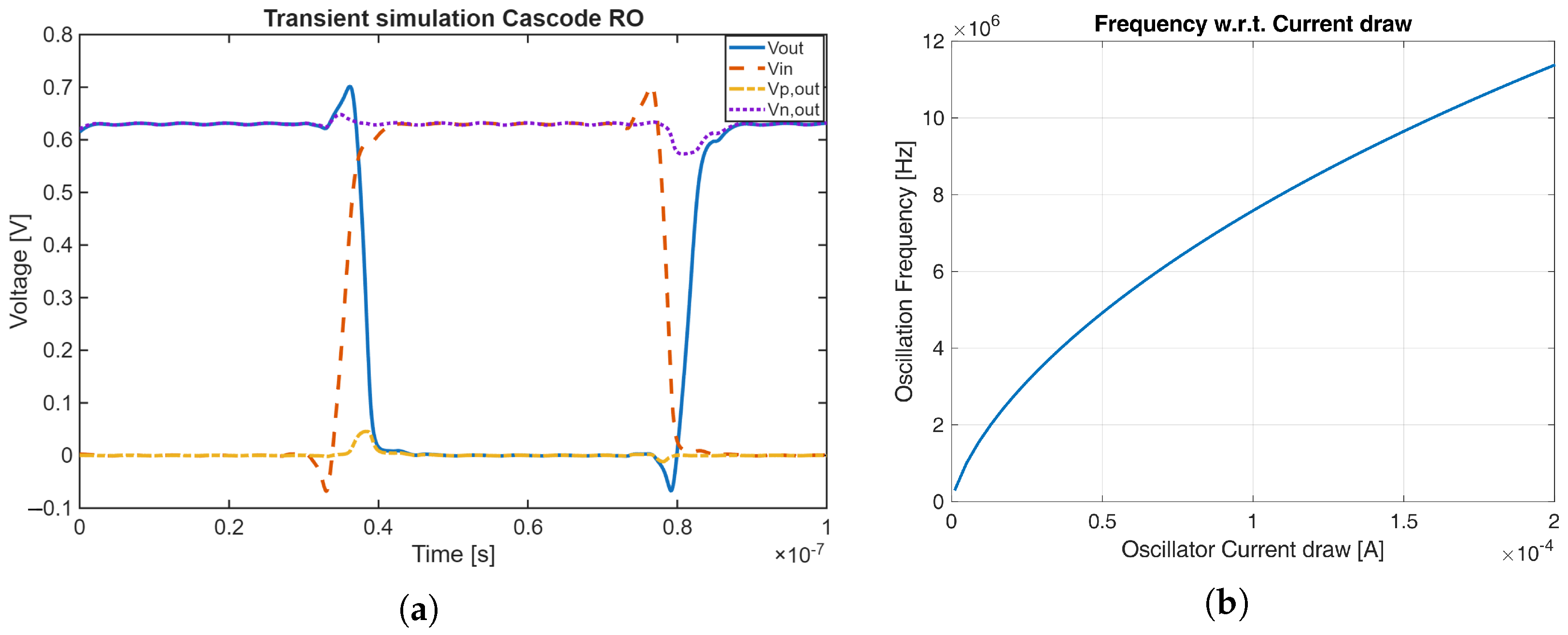
As a first simulation, the schematic transient behaviour of the novel cascode RO is included in Figure 5a. All simulations shown in this manuscript were done in a 0.13 µm CMOS node. The oscillator shown in Figure 2c is driven by a current source and referred to as GND. As seen in Figure 5a, V p , o u t and V n , o u t replicate V r i n g and GND voltages when the inverter is not in transition, with a minimal V d s voltage drop. During transition, the top PMOS and bottom NMOS devices (the cascode transistors) are biased in the triode region and act as variable resistors dependent on V r i n g . This means that the cascode transistors are active when switching, lowering the flicker contributions of the oscillator as a higher active area is available. Nevertheless, the additional active area of the cascode transistors does not increase the load significantly compared to the previous stage. Additionally, as cascode transistor V d s drop is negligible at any transient point except for the transition, and no modifications are required for the readout of the oscillator, either by level shifters or SAFFs [23]. The oscillator frequency with respect to its current draw curve is plotted in Figure 5b.

3.2. Ring Oscillator Comparison: Gain and Oscillation Frequency

Checking the differences between the ring oscillator topologies shown in Figure 2 can prove challenging, as using the same sizes in the CMOS transistors for all topologies does not result in comparable characteristics. This manuscript addresses this challenge by making a comparison of the proposed topologies based on the following principle: to use the same estimated area (calculated using active gate area), current, and voltage drop in all oscillator designs. Additionally, the number of stages is the same for all implementations, ensuring that the same oscillator readout logic can be used in all cases (note that differential ring oscillators can also be configured with an odd number of stages). By doing so, the “costs” of the oscillators are the same, and we can compare the differences in oscillation frequency, gain, noise performance, and distortion. This analysis is obtained using PSS simulations, as demonstrated in [8].
The bias current of the ring oscillators is fixed to 100 µA, their voltage drop was approximated to 1 V, and the estimated area (not considering layout implementation) was kept constant at 0.005 mm2. These parameters are aligned with ring oscillators used in VCO-ADCs for biomedical and audio applications [2,21,23]. In addition, a 10 fF capacitor was connected to each inverter, simulating the gate capacitance of the readout circuit buffers. Based on a previous analysis, the cascode inner and outer transistors have the same sizes for each PMOS and NMOS, respectively.
Table 1 gathers PSS simulation results, comparing cascode ROs with single-ended and differential feed-forward ROs. These simulations revealed an increased rest frequency and, therefore, effective frequency for the same current, voltage, and oscillator area on the cascode RO. Specifically, comparing the novel cascode RO with the single-ended RO with the same area and power, the rest frequency increases by ×1.9 times. This would result in an improvement of the SQNR of 5.6 dB, thus extending the dynamic range of the VCO-ADC. As an addition, Table 1 includes a case in which a single-ended ring oscillator is designed for the same power budget and stages as the rest, but with half the estimated area (single-ended HA). This results in an oscillator that is only slightly faster than the cascode ring oscillator but with worse flicker performance, as will be seen in the next section. The fact that the cascode ring oscillator and the half-area (HA) single-ended ring oscillator have similar frequencies validates the assumption made in Figure 4 regarding the halved load capacitance seen at each stage of the oscillator.

3.3. Ring Oscillator Comparison: Noise and Distortion

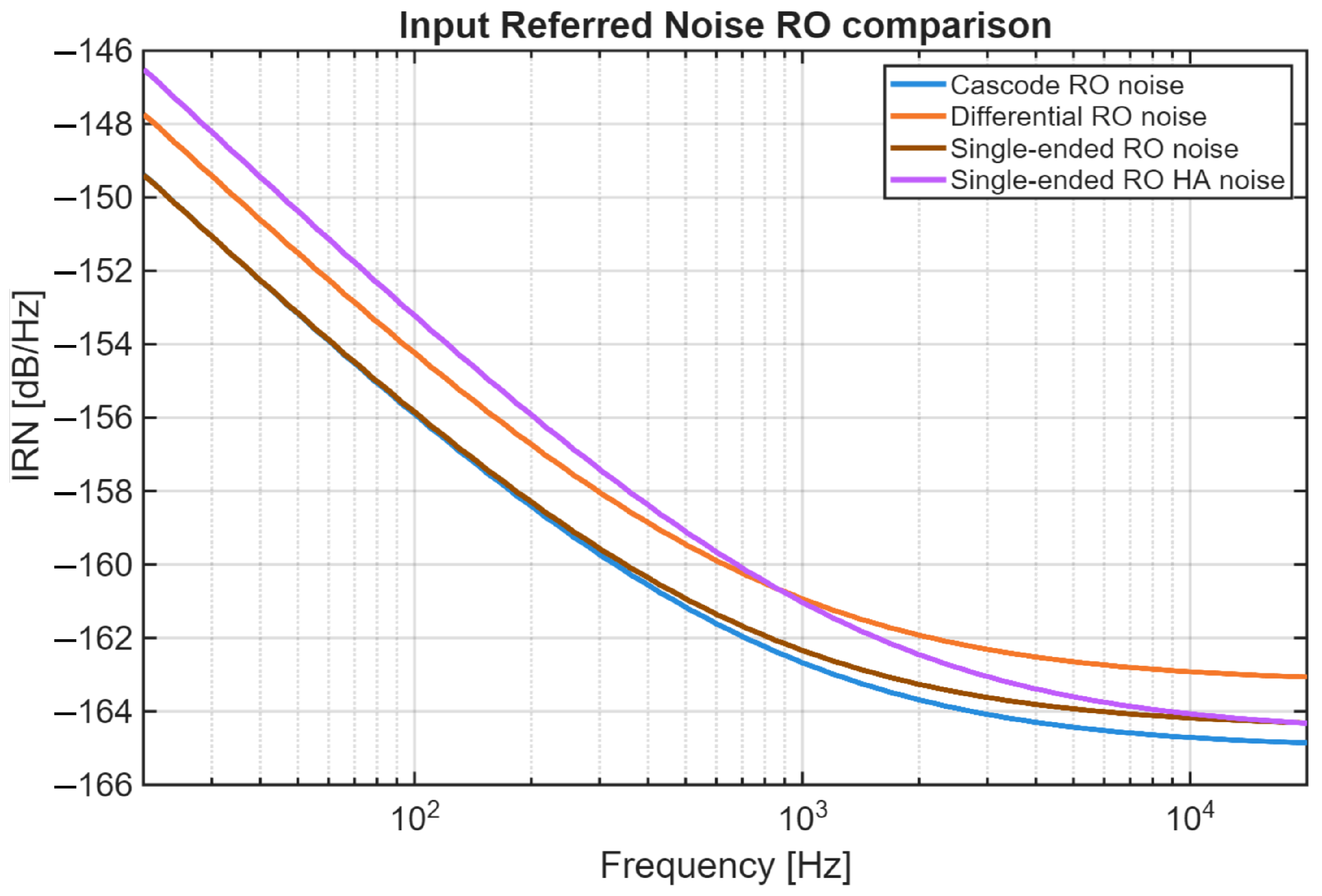
Contrary to RO implementations used for PLL or clock references, VCO-ADCs require an analysis of their phase noise referred to their input to properly infer the SNR of the converter, as demonstrated by [8]. As such, this paper shows an input referred noise (IRN) comparison in Figure 6 of the analyzed topologies, considering a bandwidth from 20 Hz to 20 kHz (biomedical and audio applications). This graph illustrates the behavior described in previous sections, where the cascode RO is able to keep flicker noise while increasing frequencies. Moreover, it is noticeable how halving the area of the single-ended HA equals the oscillation frequency at the cost of increasing flicker noise by approximately 3 dB. Notice that, in a constant current, area, and voltage comparison, the differential feed-forward RO offers lower noise performance than other architectures. This is expected given the analysis of [11].
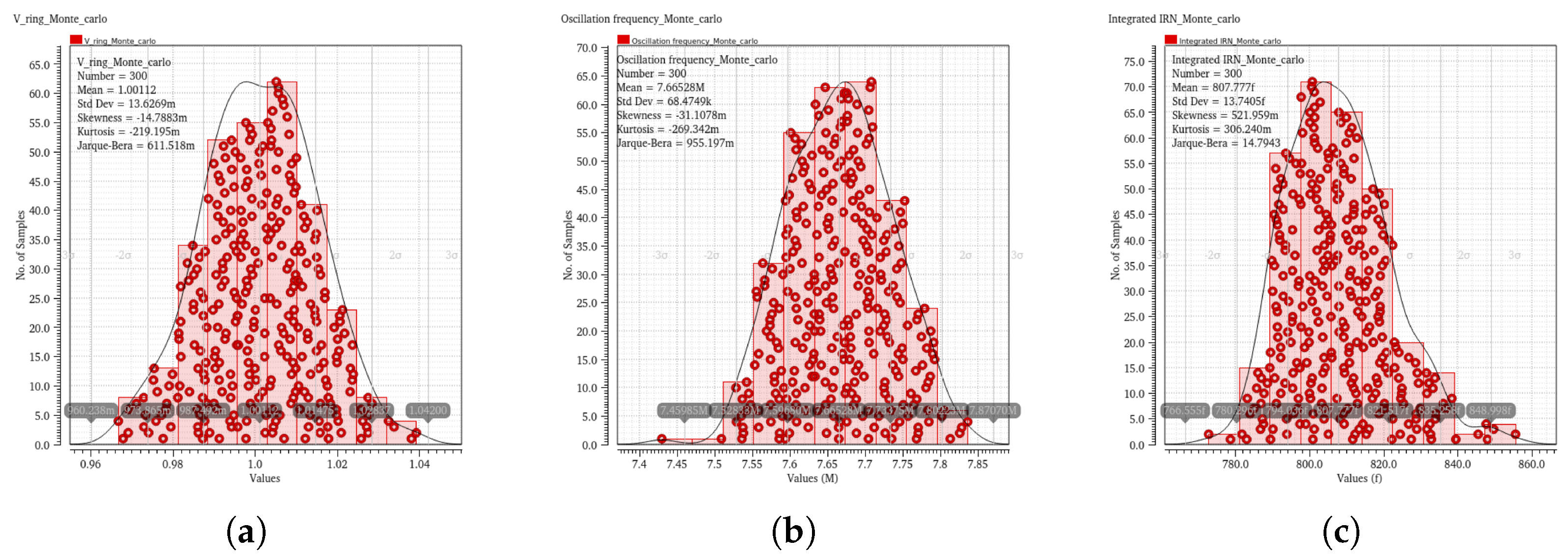
The improvement in the phase noise and oscillation frequency is maintained across process corners and Monte Carlo simulations. Table 2 summarizes the power, oscillation frequency, and integrated IRN deviations at process corners without any kind of calibration. This considers that the current draw of the oscillator is fixed at 100 µA. As seen, deviations of nominal parameters across corners are inferior by 6% in the case of integrated IRN noise (20 Hz to 20 KHz) and the oscillation frequency, and it is under 10% in the case of the voltage drop across the RO ( V r i n g ). This is confirmed by a 300-sample Monte Carlo sweep, as shown in Figure 7.
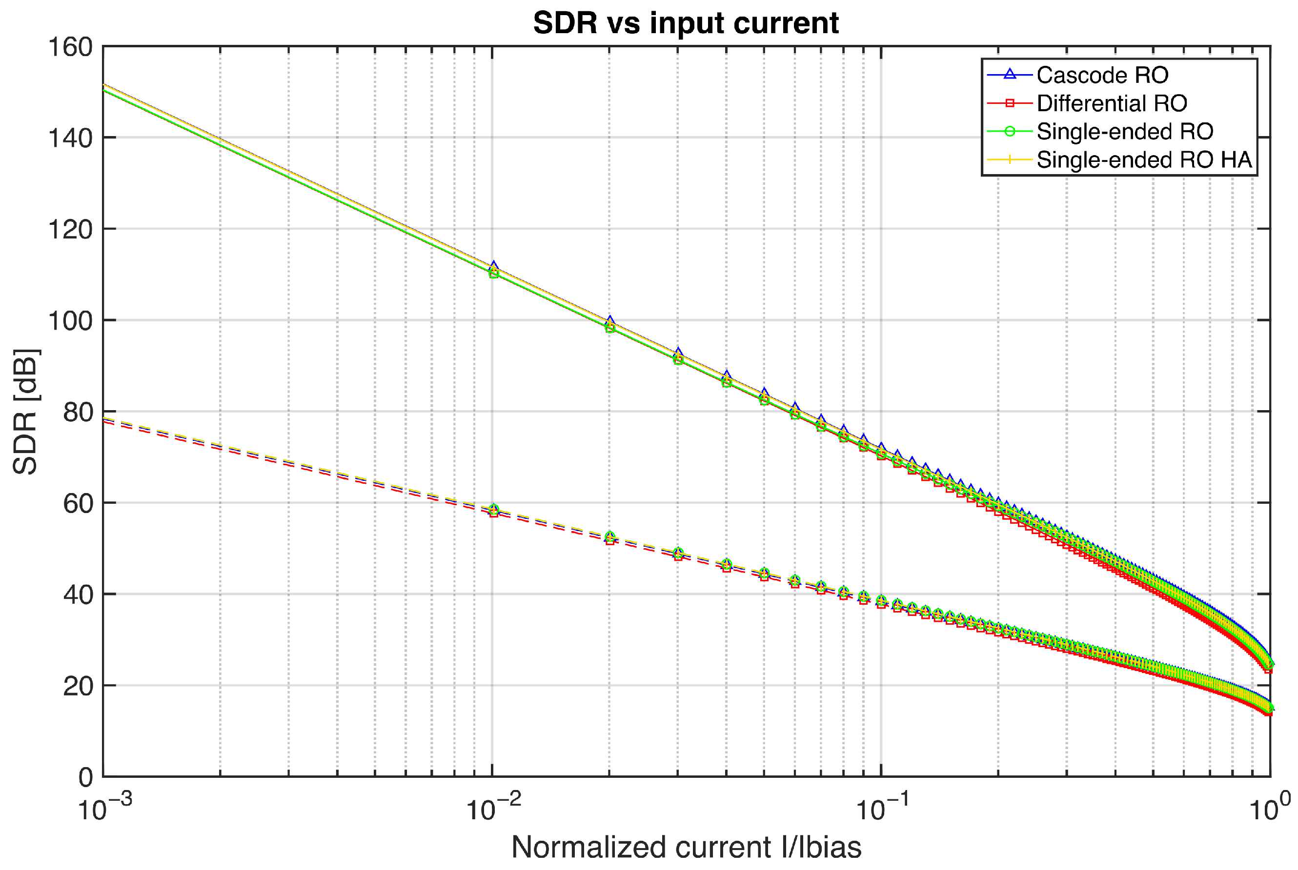
An important circuit impairment to consider in VCO-ADCs is the linearity of the VCO. We are going to compare the linearity of the cascode RO to the other circuit options as well. Figure 8 represents the signal-to-distortion ratio (SDR) of the different proposed designs. The SDR has been calculated using the tunning curve (current to frequency conversion) of every oscillator obtained in PSS simulations. The horizontal axis represents the peak current of a sinusoidal input signal normalized to the bias current (100 µA). Given the similar normalized gain ( k d = K V C O / f o ) of the proposed designs, there are no discernible differences in the SDR of the designs. The SDR is given for the ROs implemented as a single-ended VCO-ADC (only one input signal), as well as for the more common implementation using two ROs for a differential VCO-ADC (improving PSRR and common noise rejection). In the differential configuration, all oscillators remain within 2 dB of difference. In fact, the cascode RO seems the better alternative in terms of differential SDR. In any case, linearity differences seem small enough not to be a deciding factor when choosing between topologies.

3.4. Layout Implementation and Post-Layout Verification

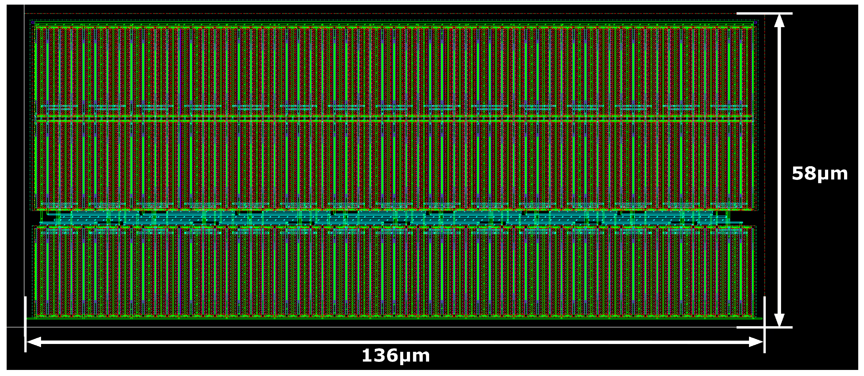
The layout of the cascode ring oscillator design of Table 1 has been implemented in a 0.13 µm process, as shown in Figure 9. The implemented area of the cascode ring oscillator is 7888 µm2. With respect to the estimated area, which considers only the active gate area, the implemented design occupies 57.8% more area than the estimation. This is due to the required space for CMOS diffusion and N-well layers, as well as the guard ring for mitigating crosstalk through substrates. This increase in area is in line with other ring oscillator designs, such as single-ended designs [21,23] and differential designs with a feed-forward structure [13,18].
A comparison between the simulation results of the cascode oscillator before and after implementing the layout is shown in Table 3. As parasitic capacitances (mainly C g s , C g d , and C g b ) are correctly accounted for in the pre-layout PSS simulations shown in Table 1, the deviation of the cascode oscillator results in post-layout simulations with respect to the pre-layout design is kept within 5.5% for all relevant parameters.

4. Discussion

Comparing the obtained results from the previous section, the cascode ring oscillator raises as an alternative to single-ended ring oscillators for VCO-ADCs commonly used in the literature. Due to its structure, it requires an odd number of inverters for oscillations, like a single-ended topology. Nevertheless, the use of a pair of cascode CMOS transistors surrounding switching internal inverters can also be implemented in direct cross-coupled and feed-forward differential ring oscillator architectures. This is especially interesting in the case of the feed-forward ring oscillator, as it would allow even faster oscillation frequencies than those obtained using the single-ended cascode cell. Additionally, these topologies could be implemented using an even number of stages and will be explored in future works.
Table 4 compares the cascode ring oscillator against other VCO designs employing ROs and relaxation oscillators in the MHz range. Across the compared solutions, the cascode ring oscillator achieves the best figure of merit with a small implemented footprint. It is also notable that ring oscillators tend to outperform relaxation oscillators in terms of phase noise, as commented by [7]. This emphasizes why they are commonly used for VCO-ADCs, although some solutions still achieve state-of-the-art performance with relaxation oscillators [26].
Considering the analysis of flicker and thermal noise given in [9,11] for different oscillator topologies, the conclusions of such papers are also applicable to the proposed novel cascode architecture. In terms of thermal noise, the cascode RO achieves slightly better performance than the single-ended RO, as seen in Figure 6. By ensuring the same power draw (voltage and current) in all cases, differences in the analytical thermal contributions of all topologies are mainly attributed to differences in the small-signal tranconductance of the ring oscillator inverters, with the topology also affecting performance slightly. Also note that, in terms of thermal noise contributions, both [9,11] analytically show that thermal noise is independent of the load capacitance (mainly, the active gate area of the next stage of the RO).
In terms of flicker (1/f) contributions of the oscillator to the IRN, the proposed new topology achieves the same performance as the single-ended architecture with the same area but increases the oscillation frequency by ×1.9 times. In Refs. [9,11], the analytical flicker contributions are proportionally dependent on the active gate area used in the RO, with a minor influence on the topology. Our phase noise results shown in Figure 6 reinforce the analytical hypothesis of [11] that flicker performance is mainly related to the active area and not topology.
As a summary, our proposed cascode RO can improve VCO-ADCs in two ways. On the one hand, if compared to a similar area and power single-ended RO, the cascode RO will deliver a higher oscillation frequency and therefore lower quantization noise for similar thermal and flicker noises. On the other hand, if compared to a smaller half-size RO with the same power, it will deliver a similar frequency and quantization noise but with lower flicker noise. The cascode RO design shown in Table 1 is suitable for low-bandwidth, low-power applications, such as biomedical and audio acquisition. Nevertheless, the cascode RO is also an interesting alternative in high-bandwidth designs given the improvement on oscillation frequency for a given area, power, and input-referred noise.

Author Contributions

Conceptualization, J.G., J.d.l.T. and L.H.; methodology, J.G. and R.G.; software, J.F. and J.d.l.T.; validation, J.G., R.G., J.d.l.T. and L.H.; formal analysis, J.G., R.G. and J.d.l.T.; investigation, J.G., R.G., J.d.l.T. and L.H.; resources, L.H.; data curation, J.G. and J.d.l.T.; writing—original draft preparation, J.G. and J.d.l.T.; writing—review and editing, J.G., R.G., J.F. and L.H.; visualization, J.G. and J.F.; supervision, R.G. and L.H.; project administration, L.H.; funding acquisition, J.G. and L.H. All authors have read and agreed to the published version of the manuscript.

Funding

This research was funded by the Spanish Ministry of Science, Innovation, and Universities, grant number FPU21/02257.

Institutional Review Board Statement

No applicable.

Informed Consent Statement

Not applicable.

Data Availability Statement

The original contributions presented in this study are included in the article. Further inquiries can be directed to the corresponding author.

Acknowledgments

The authors would like to acknowledge Ricardo Carrero Bardon for the fruitful conversations regarding the analysis and obtained results of the present manuscript. No GenAI tools were used in the analysis, data search, graphics generation, redaction, or review of this manuscript.

Conflicts of Interest

The authors declare no conflicts of interest. The funders had no role in the design of the study; in the collection, analyses, or interpretation of data; in the writing of this manuscript; or in the decision to publish the results.

Abbreviations

The following abbreviations are used in this manuscript:
CMOSComplementary Metal–Oxide–Semiconductor
DACDigital-to-Analog Converter
F2DFrequency to Digital (Converter)
FoMFigure of Merit
HAHalf Area
IRNInput-Referred Noise
MOSMetal–Oxide–Semiconductor
NMOSN-Channel Metal–Oxide–Semiconductor
PLLPhase-Locked Loop
PMOSP-Channel Metal–Oxide–Semiconductor
PSRRPower Supply Rejection Ratio
PSSPeriodic Steady State
RORing Oscillator
SAFFSensing Amplifier-Based Flip-Flop
SDRSignal-to-Distortion Ratio
SNDRSignal-to-Noise-and-Distortion Ratio
SFDRSpurious-Free Dynamic Range
SQNRSignal-to-Quantization Noise Ratio
VCOVoltage-Controlled Oscillator
VCO-ADCVoltage-Controlled Oscillator-Based Analog-to-Digital Converter

References

  1. Kim, J.; Park, S.Y. An Energy-Efficient 12-Bit VCO-Based Incremental Zoom ADC with Fast Phase-Alignment Scheme for Multi-Channel Biomedical Applications. Electronics 2024, 13, 1754. [Google Scholar] [CrossRef]
  2. Cardes, F.; Azizi, E.; Hierlemann, A. A Time-Domain Readout Technique for Neural Interfaces Based on VCO-Timestamping. IEEE Trans. Biomed. Circuits Syst. 2023, 17, 574–584. [Google Scholar] [CrossRef]
  3. Gielen, G.G.; Hernandez, L.; Rombouts, P. Time-Encoding Analog-to-Digital Converters: Bridging the Analog Gap to Advanced Digital CMOS-Part 1: Basic Principles. IEEE Solid-State Circuits Mag. 2020, 12, 47–55. [Google Scholar] [CrossRef]
  4. Kurtoglu, A.; Shirazi, A.H.M.; Mirabbasi, S.; Miri Lavasani, H. An Ultra-Low-Power 65 nm Single-Tank 24.5-to-29.1 GHz Gm-Enhanced CMOS LC VCO Achieving 195.2 dBc/Hz FoM at 1 MHz. Electronics 2024, 13, 1162. [Google Scholar] [CrossRef]
  5. Shi, Y.; Liu, X.; Hu, C.; Tang, X.; Jiang, J. A Dual Slope Boosted Relaxation Oscillator with 2.93 µJ/Cycle Energy Efficiency and 0.068% Period Jitter in 180 nm CMOS. IEEE Trans. Circuits Syst. I Regul. Pap. 2025, 72, 2520–2528. [Google Scholar] [CrossRef]
  6. Gagliardi, F.; Manfredini, G.; Ria, A.; Piotto, M.; Bruschi, P. Low-Phase-Noise CMOS Relaxation Oscillators for On-Chip Timing of IoT Sensing Platforms. Electronics 2022, 11, 1794. [Google Scholar] [CrossRef]
  7. Navid, R.; Lee, T.; Dutton, R. Minimum achievable phase noise of RC oscillators. IEEE J. Solid-State Circuits 2005, 40, 630–637. [Google Scholar] [CrossRef]
  8. Cardes, F.; Quintero, A.; Gutierrez, E.; Buffa, C.; Wiesbauer, A.; Hernandez, L. SNDR Limits of Oscillator-Based Sensor Readout Circuits. Sensors 2018, 18, 445. [Google Scholar] [CrossRef] [PubMed]
  9. Abidi, A. Phase Noise and Jitter in CMOS Ring Oscillators. IEEE J. Solid-State Circuits 2006, 41, 1803–1816. [Google Scholar] [CrossRef]
  10. Pepe, F.; Andreani, P. An Accurate Analysis of Phase Noise in CMOS Ring Oscillators. IEEE Trans. Circuits Syst. II Express Briefs 2019, 66, 1292–1296. [Google Scholar] [CrossRef]
  11. Borgmans, J.; Riem, R.; Rombouts, P. The Analog Behavior of Pseudo Digital Ring Oscillators Used in VCO ADCs. IEEE Trans. Circuits Syst. I 2021, 68, 2827–2840. [Google Scholar] [CrossRef]
  12. Gutierrez, E.; Rombouts, P.; Hernandez, L. Why and How VCO-based ADCs can improve instrumentation applications. In Proceedings of the 2018 25th IEEE International Conference on Electronics, Circuits and Systems (ICECS); IEEE: New York, NY, USA, 2018; pp. 101–104. [Google Scholar] [CrossRef]
  13. Saux, B.; Borgmans, J.; Raman, J.; Rombouts, P. A 3.5 GS/s 1-1 MASH VCO ADC With Second-Order Noise Shaping. IEEE Trans. Circuits Syst. I Regul. Pap. 2025, 72, 694–707. [Google Scholar] [CrossRef]
  14. Liu, W.; Hou, Y.; Wang, X.; Liu, Y. A 500 mVpp Input Range First-Order VCO-Based ADC with a Multi-Phase Quantizer for EEG Recording Front Ends. Electronics 2024, 13, 1483. [Google Scholar] [CrossRef]
  15. Choi, M.Y.; Kong, B.S. Linearity Enhancement of VCO-Based Continuous-Time Delta-Sigma ADCs Using Digital Feedback Residue Quantization. Electronics 2021, 10, 2773. [Google Scholar] [CrossRef]
  16. Zheng, X.; Lin, Q.; Xing, X.; Gielen, G. A 200-MHz-BW 163-dB-FoM VCO-Based MASH 3-1 ΔΣ ADC With All-Pass-Filtering Gm-C Integrator in 16-nm FinFET. IEEE J. Solid-State Circuits 2025, 1–12. [Google Scholar] [CrossRef]
  17. Noviello, M.; Quintero, A.; Paton, S. A Scalable Low-Power Time-Encoded Interface for Unbiased Capacitive Microphones. IEEE Sens. J. 2025, 25, 32942–32952. [Google Scholar] [CrossRef]
  18. Granizo, J.; Garvi, R.; Carrero, R.; Fernandez, J.; Medina, V.; Straeussnigg, D.; Wiesbauer, A.; Hernandez, L. A 381.4 µW 114dB-A DR Companding VCO-ADC for MEMS Microphones Using a Multirate Architecture. In Proceedings of the 2025 IEEE European Solid-State Electronics Research Conference (ESSERC); IEEE: New York, NY, USA, 2025; pp. 553–556. [Google Scholar] [CrossRef]
  19. Wall, A.; Walsh, P.; Sadeghipour, K.; O’Connell, I.; O’Hare, D. An Improved Linearity Ring Oscillator-Based Current-to-Digital Converter. IEEE Solid-State Circuits Lett. 2022, 5, 202–205. [Google Scholar] [CrossRef]
  20. Borgmans, J.; Sacco, E.; Rombouts, P.; Gielen, G. Methodology for Readout and Ring Oscillator Optimization Toward Energy-Efficient VCO-Based ADCs. IEEE Trans. Circuits Syst. I Regul. Pap. 2022, 69, 985–998. [Google Scholar] [CrossRef]
  21. Medina, V.; Garvi, R.; Granizo, J.; Amaral, P.; Corporales, L.H. Second-Order VCO-ADC Architecture With Low-Area and High Dynamic Range Using Internal Binary Encoding. IEEE Trans. Circuits Syst. I 2025, 72, 3072–3083. [Google Scholar] [CrossRef]
  22. Baert, M.; Dehaene, W. A 5-GS/s 7.2-ENOB Time-Interleaved VCO-Based ADC Achieving 30.5 fJ/cs. IEEE J. Solid-State Circuits 2020, 55, 1577–1587. [Google Scholar] [CrossRef]
  23. Perez, C.; Garvi, R.; Lopez, G.; Quintero, A.; Leger, F.; Amaral, P.; Wiesbauer, A.; Hernandez, L. A VCO-Based ADC With Direct Connection to a Microphone MEMS, 80-dB Peak SNDR and 438-μW Power Consumption. IEEE Sens. J. 2023, 23, 8466–8477. [Google Scholar] [CrossRef]
  24. Sacco, E.; Vergauwen, J.; Gielen, G. A 96.9-dB-Resolution 109-µW Second-Order Robust Closed-Loop VCO-Based Sensor Interface for Multiplexed Single-Ended Resistance Readout in 180-nm CMOS. IEEE J. Solid-State Circuits 2022, 57, 2764–2777. [Google Scholar] [CrossRef]
  25. Nguyen, T.V.H.; Pham, C.K. A Dual-Mode Adaptive Bandwidth PLL for Improved Lock Performance. Electronics 2025, 14, 4008. [Google Scholar] [CrossRef]
  26. Cardes, F.; Gutierrez, E.; Quintero, A.; Buffa, C.; Wiesbauer, A.; Hernandez, L. 0.04-Mm2 103-dB-A Dynamic Range Second-Order VCO-Based Audio ΣΔ-ADC in 0.13-µm CMOS. IEEE J. Solid-State Circuits 2018, 53, 1731–1742. [Google Scholar] [CrossRef]
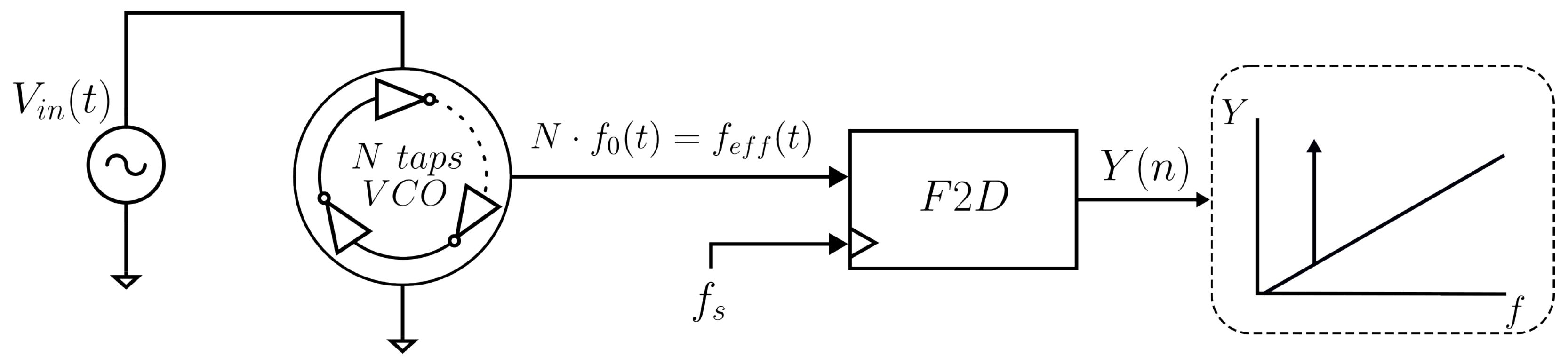
Figure 1. Block diagram of a VCO-ADC architecture.
Electronics 15 02299 g001
Figure 2. Schematic RO architectures: (a) an N-stage RO single-ended structure, (b) an N-stage differential RO with a feed-forward structure, and (c) an N-stage RO based on a cascode topology.
Electronics 15 02299 g002
Figure 3. (a) Single-ended ring oscillator controlled by a current-starving driver. (b) Proposed cascode RO being driven by a current or voltage driver. The orange path represents the electrical connections of the cascode PMOS transistors, and the blue path the electrical connections of the cascode NMOS transistors.
Electronics 15 02299 g003
Figure 4. Load capacitance comparison in a (a) single-ended RO cell and (b) cascode RO cell.
Electronics 15 02299 g004
Figure 5. (a) Cascode RO falling and rising edge transitions over time. (b) Frequency with respect to the current draw of the cascode oscillator; parameters shown in Table 1.
Electronics 15 02299 g005
Figure 6. Input referred noise of different ROs.
Electronics 15 02299 g006
Figure 7. Monte Carlo analysis of the parameters of the proposed cascode RO: (a) V r i n g , (b) oscillation frequency, and (c) integrated input referred noise.
Electronics 15 02299 g007
Figure 8. SDR w.r.t normalized current. The differential SDR is represented by solid lines, and the single-ended SDR is represented by dashed lines.
Electronics 15 02299 g008
Figure 9. Layout and dimensions of the proposed ring oscillator with cascoded inverter delay cells.
Electronics 15 02299 g009
Table 1. Oscillator performance comparison.
OscillatorsEstimated Area a [µm2]Current ( i bias ) [µA] V ring [V] f 0 [MHz] K VCO [MHz/V] k d [ V 1 ] f eff [MHz]
Cascode50001001.0017.5916.22.13114
Single-ended50001000.9983.998.172.0559.8
Differential
feed-forward
50001000.9964.338.501.9764.9
Single-ended HA25001000.9967.8216.12.06117
a Calculated using active gate area.
Table 2. Effect of process corners in the cascode ring oscillator.
Process Corner V ring [V]Deviation from Nominal f 0 [MHz]Deviation from NominalIntegrated IRN [ fV 2 ]Deviation from Nominal
Nominal1.001-7.59-801.4-
Fast0.912−8.9%8.005.4%767.1−4.3%
Slow1.0929.1%7.22−4.9%846.65.6%
FS1.0111.0%7.51−1.1%805.70.5%
SF0.990−1.1%7.701.4%776.9−3.1%
Table 3. Cascode oscillator schematic versus post-layout comparison.
OscillatorsArea [µm2]Current [µA] V ring [V] f 0 [MHz] K VCO [MHz/V] k d [ V 1 ] f eff [MHz]
Pre-layout5000 a1001.0037.5916.22.13114
Post-layout78881001.0067.1715.42.14108
Difference57.8%0%3.0%−5.5%−4.9%0.1%5.0%
a Calculated using active gate area.
Table 4. Comparison with the state-of-the-art VCOs.
This WorkThis WorkIEEE JSSC a 2022 [24]MDPI Electronics b 2025 [25]IEEE TCAS I 2025 [5]MDPI Electronics 2025 [6]
Process [nm]130130180180180180
TypeCascode ROSingle-ended ROSingle-ended ROCurrent-starved RORelaxation w. DSBRelaxation w. CSTA
Frequency [MHz]7.593.991.51800210
Power [µW]10010016.423005.8650.8
Area0.0080.005 c0.0070.0350.102
FoM d 1 kHz [dBc/Hz]169.0168.5156.1140.7 152.1
FoM d 100 kHz [dBc/Hz]171.4170.1156.7160.7148154.4
a Values extracted from figures (measurements). b Values extracted from figures (simulations). c Estimated using active gate area. d FoM = −PN + 20log10(fo/Δf) − 10log10 (Power/1 mW).
Disclaimer/Publisher’s Note: The statements, opinions and data contained in all publications are solely those of the individual author(s) and contributor(s) and not of MDPI and/or the editor(s). MDPI and/or the editor(s) disclaim responsibility for any injury to people or property resulting from any ideas, methods, instructions or products referred to in the content.