1. Introduction
The concept of quantum computing was first proposed by Richard Feynman in the 1980s, who suggested that quantum computers could effectively solve complex problems in physics and chemistry [
1]. In 1994, Shor developed the quantum factorization algorithm [
2], demonstrating a breakthrough in large integer factorization that posed a potential threat to RSA encryption. Subsequently, in 1996, Grover’s search algorithm further advanced research in quantum computing [
3]. In recent years, with the rapid development of quantum computer technology, quantum science has become a major research focus worldwide, covering areas such as quantum computing, quantum communication, quantum finance, and quantum algorithms. Unlike classical computers that operate on binary bits of 0 and 1, quantum computing is based on the principles of quantum superposition and quantum entanglement, enabling massive parallelism. This allows quantum computers to address problems beyond the capabilities of supercomputers, including cryptography, machine learning, weather forecasting, materials science, and drug discovery [
4,
5,
6,
7,
8,
9].
With the advancement of quantum communication technology, combined with the threat of Shor’s quantum factorization algorithm to RSA encryption [
2], existing cryptographic systems face significant challenges. Current cryptographic techniques are primarily divided into symmetric encryption (e.g., DES, 3DES, AES) and asymmetric encryption (e.g., RSA) [
10]. Among these, AES (Advanced Encryption Standard) is the most widely used, with applications in communication, data storage, and cybersecurity. Although AES is considered highly secure under present-day technology, the rapid development of quantum computing may compromise its strength, and brute-force attacks on AES could become feasible in the future [
11]. In light of these developments, researchers have begun exploring new cryptographic systems, including post-quantum and quantum-inspired cryptographic systems [
12].
Quantum cryptography is developed based on the principles of quantum mechanics and is characterized by extremely high security, making it nearly impossible for unauthorized parties to access or compromise shared and protected data. The most prominent and mature application of quantum cryptography is Quantum Key Distribution (QKD) [
13]. QKD employs quantum communication techniques to allow two communicating parties (commonly referred to as Alice and Bob) to securely share a symmetric key.
With the rapid development of network communication technologies, digital images can be transmitted anytime and anywhere, making image encryption increasingly important and privacy protection a focal point of public concern. Quantum image encryption (QIE), as a branch of quantum cryptography and quantum information processing (QIP), aims to secure image information using quantum techniques. Compared with plain digital data, image data conveys richer information, and studies have shown that human memory for images is superior to that for text, further highlighting the necessity of image information security [
14,
15]. This technology can be applied to various sensitive scenarios, such as protecting patients’ medical imaging records, transmitting private photos, or securely conveying classified images of enemy positions in military operations. Although research in this field is still developing, it has already become a critical topic in information security.
In 2003, Beach et al. applied Grover’s quantum search algorithm to image processing [
16]. In the same year, Venegas et al. introduced the concept of quantum image processing [
17], formally initiating the development of this field. In subsequent years, researchers proposed using entangled states to store the positions and grayscale values of images. Several quantum image processing methods have since been developed. For example, in 2011, Phuc Q. Le et al. proposed the Flexible Representation of Quantum Images (FRQI) [
18], designed for polynomial preparation, image compression, and processing. Simulation experiments using FRQI included image storage, retrieval, and the detection of lines in binary images via quantum Fourier transform operations. In 2013, Zhang et al. proposed a Novel Enhanced Quantum Representation (NEQR) [
19], improving upon the FRQI by storing each pixel’s grayscale value directly in the computational basis of qubit sequences, rather than encoding them in probability amplitudes as in FRQI. Comparisons with FRQI showed that NEQR enables quadratic acceleration in quantum image preparation, increases image compression by approximately 1.5 times, and allows accurate retrieval of digital images from quantum representations. As research on quantum image models progressed, numerous algorithms for quantum image operations and processing were developed, including quantum image filtering, quantum edge detection, and quantum image encryption algorithms. For instance, in 2021, Jinlei Zhang et al. proposed splitting image data into multiple parts for encryption [
20]. Other researchers suggested mapping RGB image data separately onto quantum circuits for encryption [
21], which, however, requires preparing 24 qubits, incurring relatively high resource costs. Some methods also employed XOR operations for image encryption [
22]. Nevertheless, these approaches typically focus on encrypting images that have already been captured.
Research has shown that integrating digital image processing with quantum computing techniques can accelerate quantum image processing. However, existing quantum image encryption methods predominantly target post-capture images, which require considerable hardware resources and processing time. Real-time image encryption, on the other hand, has broader applications, such as protecting sensitive geographic data captured by military drones or safeguarding personal privacy in security surveillance systems. Some researchers have proposed a real-time image transmission technique for drones, implemented using a Raspberry Pi [
23]. Compared with MCUs, one of the key advantages of FPGAs is their programmable architecture, which allows designers to quickly and repeatedly reconfigure them for different functions, while also offering low latency, low power consumption, and strong parallel processing capabilities [
24].
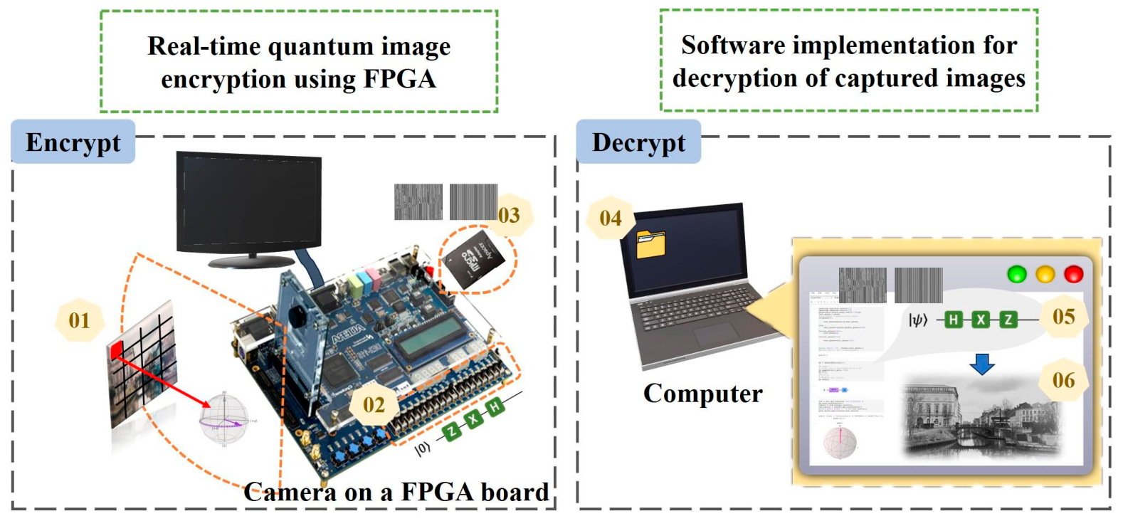
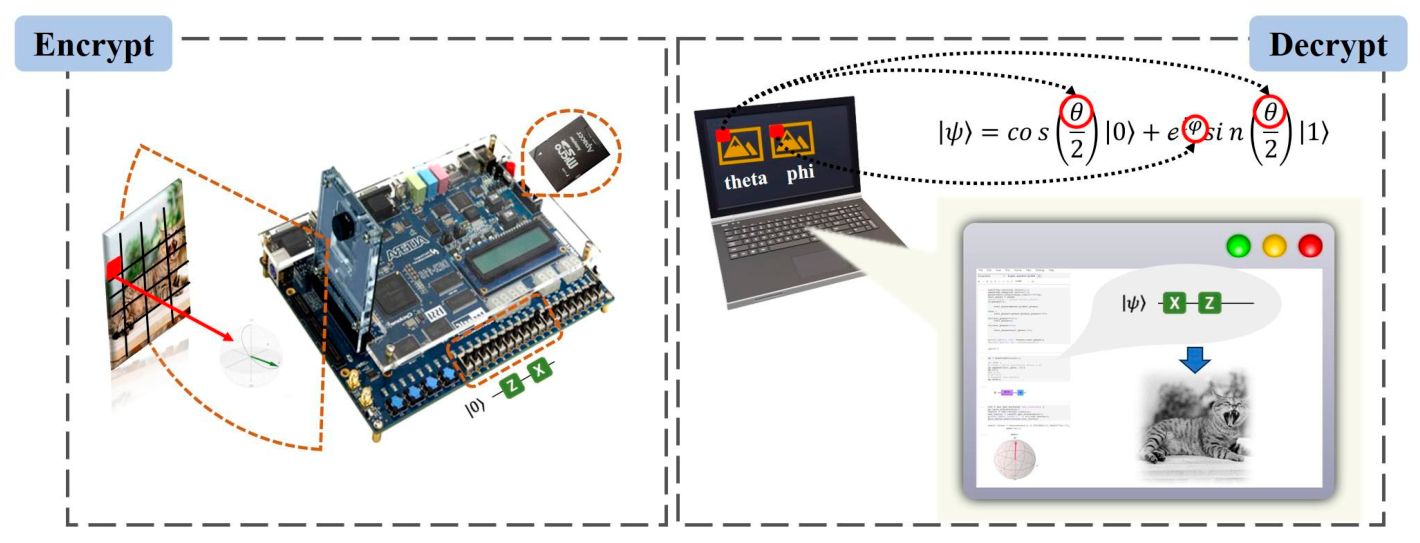
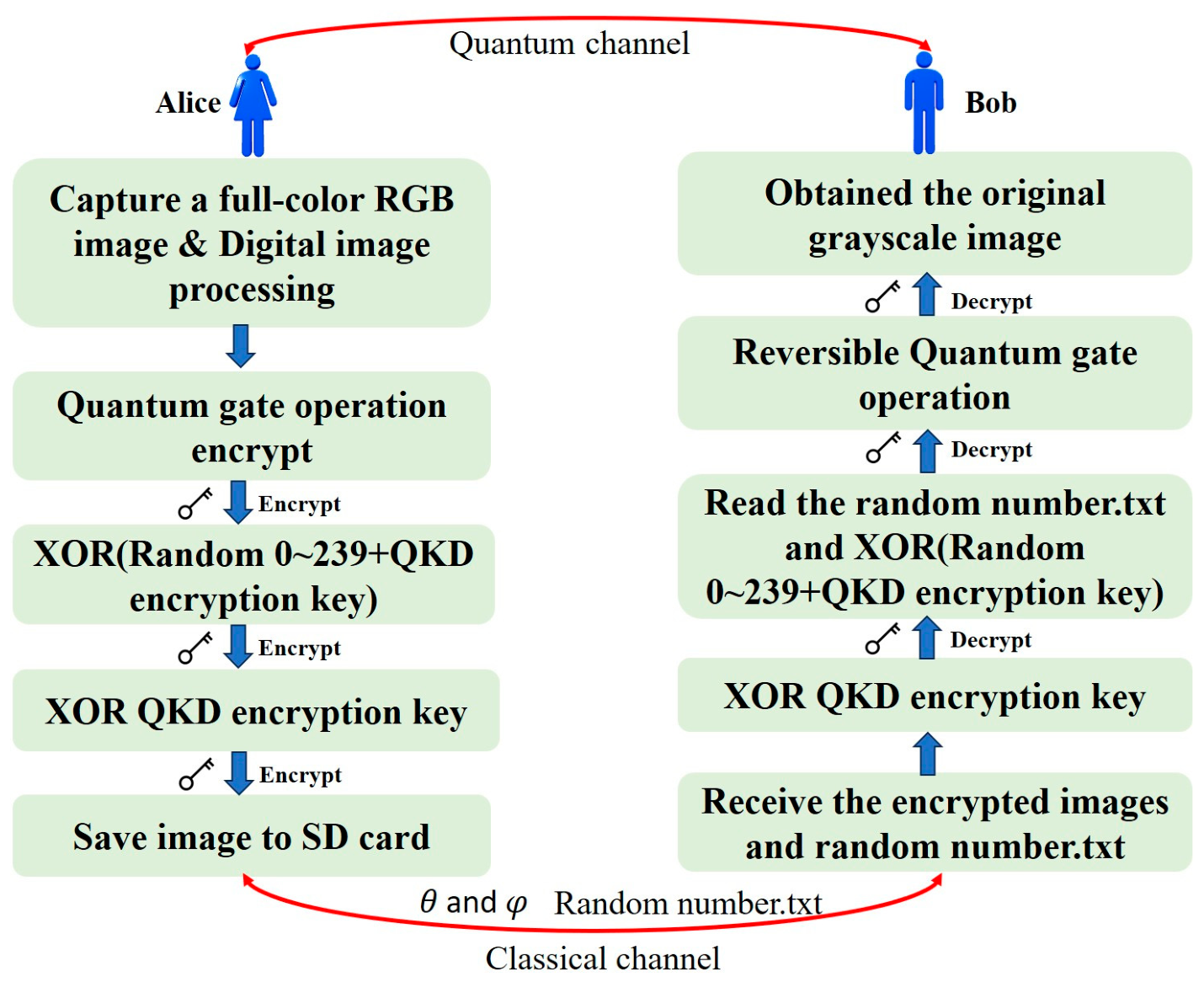
Based on the reversible nature of quantum computation compared to classical computation, this study proposes an innovative image encryption method. The method employs reversible quantum gates to perform image encryption and decryption, establishing a real-time image encryption system. This system enhances security and efficiency during image transmission and leverages the unique properties of quantum computation to significantly improve the reliability of data protection, offering a practical solution for future image privacy protection. Real-time image acquisition is performed using a CMOS camera module, and encryption processing is executed on an FPGA. The processed images are subsequently stored on an SD card. Finally, by leveraging the reversibility inherent to quantum computation, the encrypted images can be decrypted on a classical computer using the proposed software-based quantum image encryption and decryption algorithm, thereby recovering the original captured images, as illustrated in
Figure 1.
This study represents a significant advancement, building upon our previous research [
25,
26]. While Reference [
25] established the foundational framework through a software-based algorithmic implementation, and Reference [
26] introduced an initial hardware prototype. The image’s pixel values are mapped at the beginning as the initial state into the quantum circuit of the qubit. We initialized the quantum state according to each pixel’s value and applied reversible quantum gate to the quantum state for image encryption. The quantum state after quantum gate operation can be calculated and implemented on the FPGA. However, these earlier approaches exhibited limitations in reconstruction performance, particularly in terms of Peak Signal-to-Noise Ratio (PSNR), which was not sufficiently high for high-quality image recovery. This approach aligns with the growing trend of practical quantum cryptography. For example, Zhang et al. demonstrated the implementation of stable, real-time key extraction within QKD systems using FPGA architectures, which addresses a critical bottleneck in practical deployments [
27]. Similarly, Gandelman et al. recently introduced a cost-effective experimental platform that uses pulsed lasers to emulate the B92 protocol, emphasizing the accessibility of hands-on, quantum-inspired systems [
26]. Unlike the focus on underlying security key generation in [
27,
28], our work focuses on the application-level integration of these concepts. Specifically, we have developed a robust XOR encryption/decryption circuit that seamlessly integrates quantum gate operations with the BB84 quantum key distribution (QKD) protocol. This hardware-level integration notably enhances both image obfuscation and cryptographic security. Compared to earlier iterations, the proposed system demonstrates superior practical feasibility and provides a more rigorous defense mechanism for secure data transmission.
The remainder of this paper is organized as follows.
Section 2 introduces the Quantum computing algorithms employed along with their theoretical foundations.
Section 3 details the proposed FPGA hardware resources, system architecture, and algorithmic design.
Section 4 presents the experimental results. Finally,
Section 5 and
Section 6 conclude the paper and outline possible directions for future work.
3. Quantum-Inspired Image Encryption Circuit Design Based on FPGA
This section describes and discusses the methods used in this study. Our design uses reversible quantum gate computation to implement a real-time quantum-inspired image encryption system on an FPGA. This includes digital image processing, reversible quantum computation, and quantum circuit design for encrypting and decrypting images. In our study, we utilized Terasic’s TRDB_D5M camera module (Terasic Inc., Hsinchu County, Taiwan) for image acquisition [
31]. This module features a 5-megapixel CMOS sensor, supports a full-resolution frame rate of up to 15 frames per second (FPS), and outputs images in the RGB Bayer pattern format. The Altera DE2-115 FPGA development board (Terasic Inc., Hsinchu County, Taiwan) [
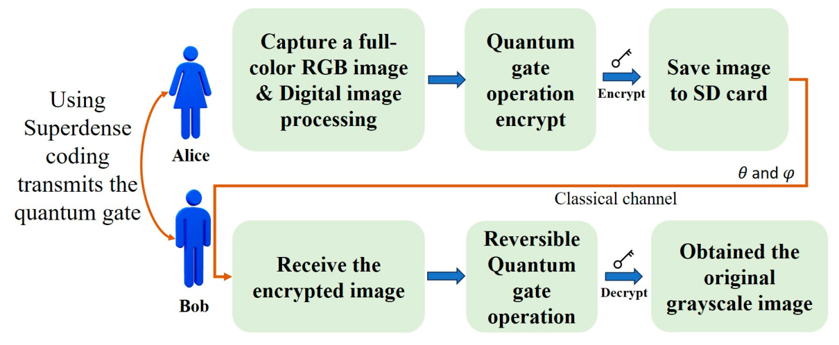
32] is used for a variety of data processing tasks, including digital image processing, quantum gate-based encryption, and storing images on an SD card. This DE2-115 FPGA is equipped with the Cyclone EP4CE115, the highest-capacity chipset in the Cyclone IV E-series, which offers 114,480 logic elements (LEs) and data transfer rates of up to 3.9 Mbps. These features significantly enhance processing speed, ensuring strong protection of image data and information security. The overall system architecture of the study is illustrated in
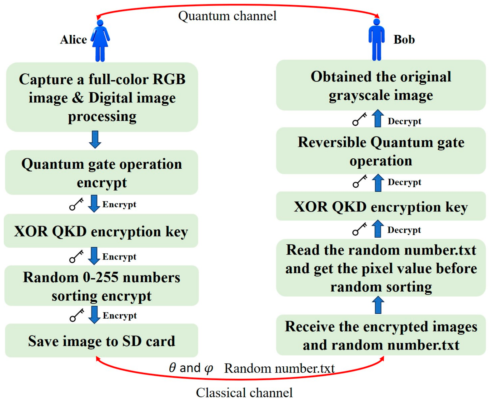
Figure 5.
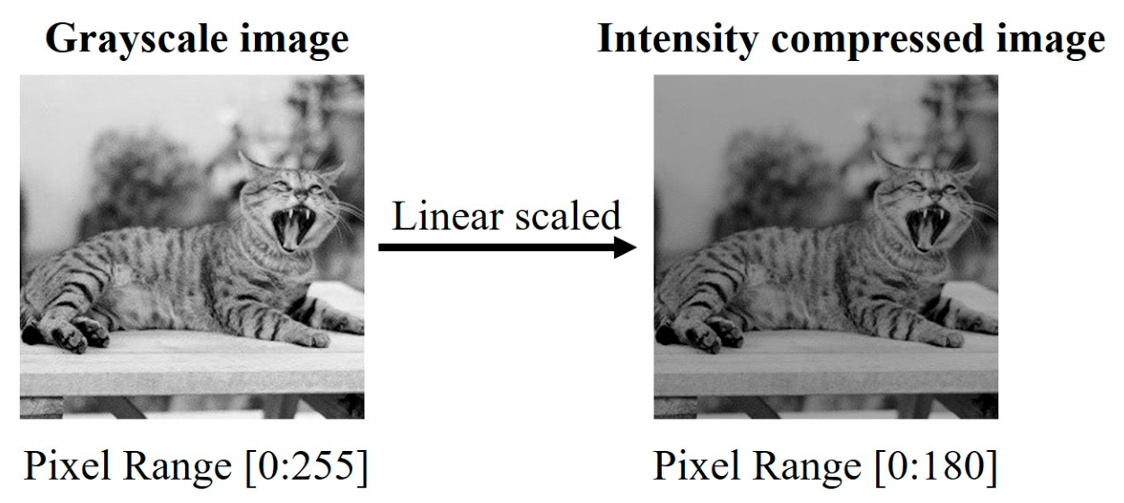
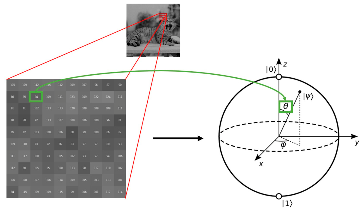
Initially, a full-color RGB image is captured using the TRDB_D5M device (Terasic Inc., Hsinchu County, Taiwan). This image is then converted into a grayscale map and linearly compressed using DE2-115. Next, the pixel values of the image are extracted and mapped to a quantum circuit, representing the initial quantum state. The image is encrypted through quantum gate operations using the buttons on the DE2-115 FPGA board (Terasic Inc., Hsinchu County, Taiwan). The encrypted image is subsequently saved to an SD card. During the decryption process, a computer retrieves the encrypted image and acquires the initial vectors via a reversible logic gate operation. The decrypted image is generated by linearly zooming in on the processed image. During the transfer process, Alice can utilize communication methods such as superdense coding to convey the information about the utilized gate to Bob. Bob can then decrypt the encrypted image using a reversible logic gate operation. The proposed system is designed to be compatible with quantum communication protocols. In theory, Alice could use superdense coding to send quantum gate information to Bob. However, it should be noted that while
Figure 5’s flow incorporates these roles to illustrate a comprehensive security framework, this paper’s core contribution lies in the hardware implementation of quantum-inspired encryption and decryption on a classical FPGA [
33,
34]. The “quantum channel” and its associated protocols are presented as a conceptual integration that demonstrates the scalability of the proposed system for end-to-end secure transmission when paired with future quantum communication technologies [
35].
3.1. Hardware Architecture
The following sections describe the configuration and functions of each device in the system.
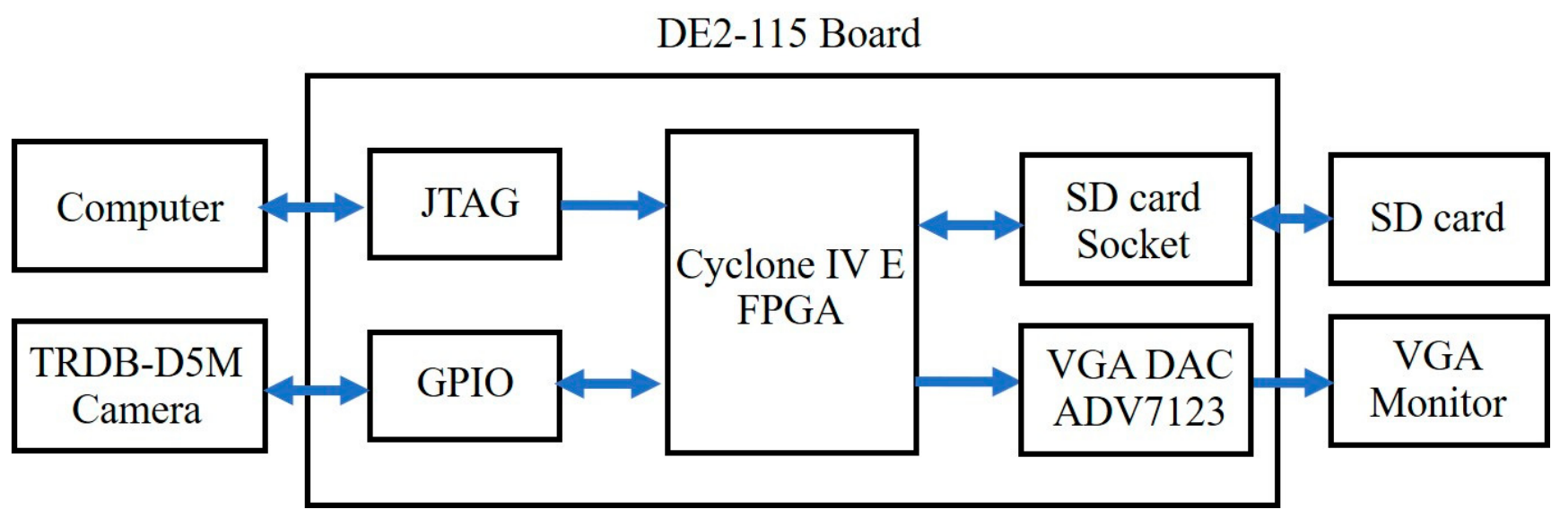
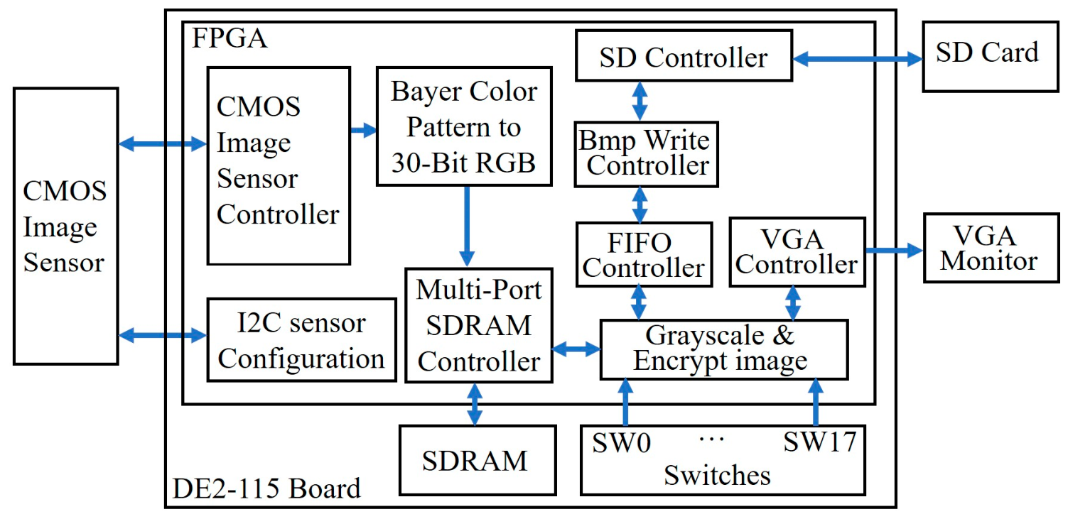
Figure 6 illustrates the hardware block diagram, which outlines the structural relationships between the various components in the system. The core component of the system is the Cyclone IV E FPGA (Altera Corporation, San Jose, CA, USA), which is responsible for executing various computational tasks and commands while communicating with other devices. Next is the main memory (SDRAM), which provides storage space, enabling the FPGA to access and manipulate data efficiently and exchange information with other system components. Additionally, the TRDB-D5M camera handles image acquisition, the VGA monitor displays the encrypted images for real-time visualization, and the SD card stores the encrypted images. The programming interface connects to the PC using a USB cable connected to the JTAG interface of the FPGA. In this study, Quartus version 17.1 was utilized for system design, and Verilog, a hardware description language (HDL), was used for designing FPGA RTL circuits. Overall, the hardware block diagram in
Figure 6 demonstrates the interconnections between the system’s devices, ensuring the implementation of various system functions.
3.2. The Top-Level Module
In the previous section, we explained the connection architecture among the various devices in the system. In this section, we will discuss the design of each module in the system. The primary data flow in the top-level module is illustrated in
Figure 7. As shown in
Figure 7, when the D5M camera (CMOS Sensor) captures image data, the data is transmitted to the FPGA. The raw data is then processed by the Bayer color-to-RGB module, converting it into RGB signals, which are stored in SDRAM. Subsequently, the stored data is retrieved from the SDRAM for image processing and quantum gate encryption operations (Grayscale and Encrypt image using Quantum Gate). The processed signals are simultaneously output to a VGA monitor at the standard video resolutions 800 × 600@60 Hz.
Additionally, switches on the DE2-115 development board are used to select different quantum gates for encryption operations. After selecting a quantum gate, the switches on the DE2-115 board are also used to trigger the SD card storage process, saving the encrypted image to the SD card. Each module is designed using Verilog. The design of the module responsible for converting D5M camera data into RGB signals is based on the open-source resources provided by Terasic. Therefore, this study primarily focuses on introducing custom-designed and integrated modules. Detailed designs for each module will be discussed in subsequent sections.
3.3. The Image Processing
As described in
Section 2.1, a quantum state
simultaneously encompasses two angles,
θ and
φ. In the quantum image encryption system, the grayscale values of the image are used as the
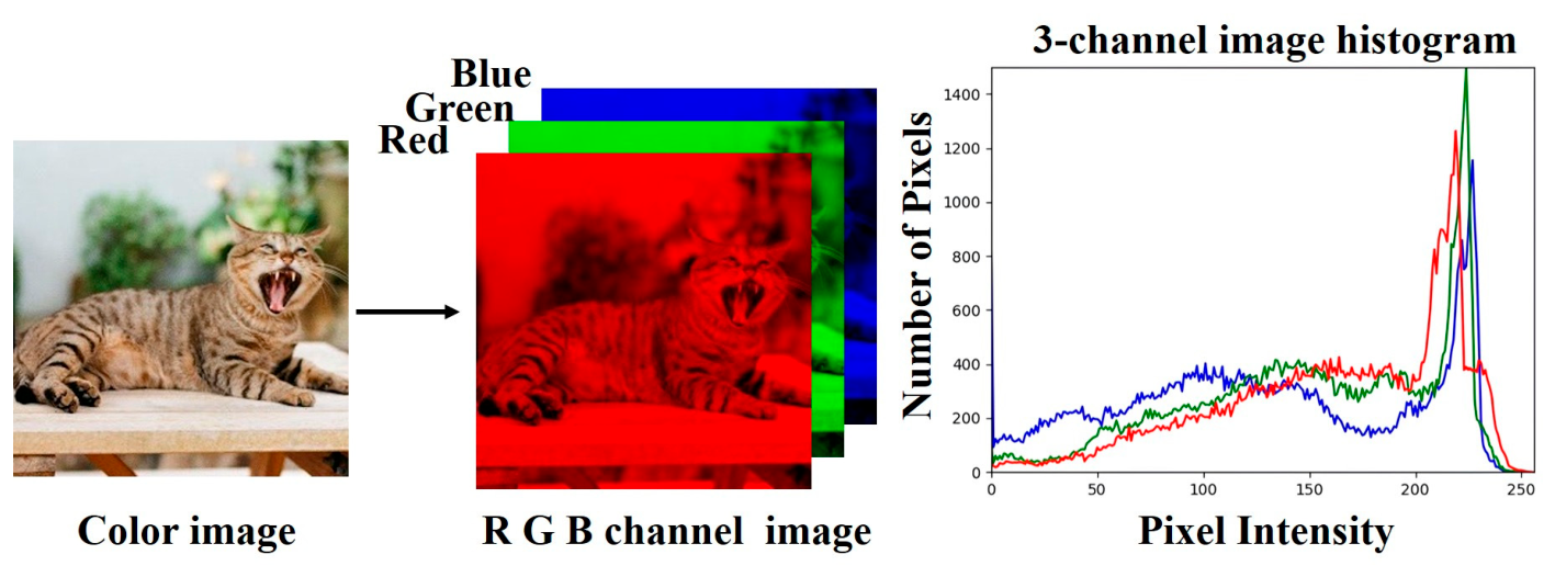
θ data to prepare the initial quantum state, which is then mapped into the quantum circuit for subsequent quantum logic encryption operations. Since floating-point computations on FPGA consume a significant number of logic elements, the RGB pixel values for each channel were pre-calculated in Excel during the design of the color-to-grayscale conversion process, with rounding applied to simplify the computations. The grayscale conversion was implemented on the FPGA using a lookup table (LUT) based design. Given that the range of
θ is between
to
, the grayscale values (range from 0 to 255) were linearly compressed to a range of 0 to 180. This linear transformation was also realized using a LUT-based FPGA design.
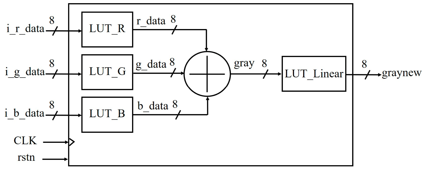
In terms of circuit design, as shown in
Figure 8, the clock (CLK) is set to 40 MHz, and the i_r, i_g, and i_b RGB image signals are output from the SDRAM. Since the images are displayed on a VGA monitor and saved to an SD card, the most significant 8 bits of these signals are extracted for subsequent image processing. Using a LUT design, the image is converted to grayscale and linearly compressed, ensuring the resulting image values fall within the range of 0 to 180. As shown in
Figure 8, CLK is Clock signal, rstn is reset signal, i_r_data is 8 bits image red channel signal, i_g_data is 8 bits image green channel signal, i_b_data is 8 bits image blue channel signal, gray is converted image signal, and i_r_data, i_g_data i_b_data are the 8 bits Image channel input for LUT_R, LUT_G, LUT_B modules, respectively. The r_data, g_data, and b_data are output for LUT_R, LUT_G, LUT_B modules, respectively. LUT_R, LUT_G, LUT_B output 0.299 × i_r_data, 0.587 × i_g_data, 0.114 × i_b_data with in lookup tables, respectively. The grayscale conversion and linear compression are implemented with LUT-based FPGA designs, as outlined in
Table A1.
The RGB channels correspond to the LUT_R, LUT_G, and LUT_B modules, while the linear compression is implemented using the LUT_Linear module described in
Table A1. So far, this section has explained how to process captured images, including converting full-color images to grayscale and applying linear compression for the design of the subsequent encryption circuit. The following section will discuss the design of the quantum image encryption circuit.
3.4. The Quantum Image Encryption Circuit Design
In hardware design for real-time image encryption, beyond considerations of resource efficiency and encryption speed, it is crucial to acknowledge the profound role of images in human life. Images serve not only as mediums of communication but also as essential tools in art, science, and education, enabling the comprehension of complex and abstract concepts. Their ability to convey rich information across linguistic and cultural boundaries highlights their irreplaceable significance. Accordingly, this work proposes and analyzes several design approaches aimed at achieving effective image encryption. The following sections provide a detailed introduction to these methods.
3.4.1. Encryption and Decryption Circuit Combining Quantum Gate Operations and Quantum Key Distribution
In the present study, due to the constraints imposed by SDRAM resources, an image with a resolution of 800 × 600 pixels was selected for the experiment. Initially, this full-color image was converted to grayscale, followed by numerical scaling. The pixel values derived from the image were then mapped onto the quantum circuit to represent the initial quantum bit state. During this mapping process, the phase angle φ of the initial quantum bit was set to 0, while the pixel value served as the value for θ. In the realm of quantum computation, the state of a quantum system can be accurately represented through vectors and matrices, along with their corresponding operations. When the phase φ of the initial quantum qubit is determined to be 0, it becomes possible to infer the quantum state after the application of the quantum gate on the initial quantum qubit. This process can be effectively implemented on the FPGA utilizing designs based on adders and subtractors.
The switches on the DE2-115 board serve as inputs for various quantum gates, which are used to perform quantum gate operations for encrypting images. The resulting encrypted ciphertexts correspond to two images representing the quantum states θ and φ after the quantum gate operation. These ciphertexts are subsequently saved in BMP file format on the SD card. Alice can use superdense coding to communicate information about the logic gates employed to Bob, while simultaneously sending the encrypted ciphertext image through a secure classical channel. Bob can then access the ciphertext image on his computer and proceed to decrypt it by applying reversible logic gate operations.
Three quantum gates—specifically, the Pauli X gate, Pauli-Z and Pauli-X gates, and Hadamard gate—are utilized to implement the encryption circuit. Regarding the process of image decryption, two ciphertext images containing the parameters
θ and
φ are first retrieved using a computer. The pixel values from these images are then mapped onto the quantum circuit to prepare the initial quantum state. The original linearly compressed image pixel
θ values can be recovered through the operations of the reversible quantum logic gate. Finally, the original grayscale image is restored through linear scaling, as illustrated in
Figure 9.
As previously mentioned, we employ quantum gate operations to encrypt image data, thereby obscuring the original content. However, it is crucial to note that encrypted images retain certain characteristics that may allow observers to infer potential information from the original image through visual interpretation or speculation. Human vision is inherently sensitive to various features within images [
26]. To enhance encryption security and prevent malicious parties from intercepting random key text (.txt) files transmitted over classical channels, we further integrate quantum key distribution (QKD) technology (such as technology based on the BB84 protocol) into the design of the encryption circuit. The encryption procedure is summarized in Algorithm 1.
| Algorithm 1. Image encryption using quantum gate operations and QKD |
1: Input: RGB image P, QKD encryption key KQKD, random sequence R, quantum gate G
2: for angle in (θ, φ) do
3: Initialize the angle to 0 for φ
4: for each image pixel P(i) do
5: Convert P(i) into a grayscale image ccording to Equation (7)
6: Initialize the angle according to Equation (8) for θ
7: Apply quantum gate operation encryption according to the rules in Table 1 to get Q(i)
8: Perform XOR encryption using the QKD secret key: X(i) = Q(i) ⊕ KQKD
9: Apply random number encryption with a look up table: C(i) = LUT(X(i), R(i))
10: end for
11: Store the encrypted image C at the corresponding address on the SD card
12: end for
13: Output encrypted θ image and encrypted φ image |
As shown in
Figure 10, when Alice executes quantum gate operations via switches on the FPGA development board, we similarly utilize the board’s switches to input the BB84 random key. Alice can easily input the QKD random key via the switches. As shown in
Figure 10, the quantum-gated encrypted image pixels undergo XOR operations with the BB84 random key to achieve secondary encryption. The QKD random key is transmitted to Bob via the quantum channel. The security of quantum key distribution has been validated in [
11], demonstrating resistance to eavesdropping and tampering. Next, a set of numbers between 0 and 255 is randomly sorted using Python in Visual Studio Code 1.118 software. Subsequently, an FPGA design based on lookup tables (LUTs) maps the image pixels processed by the quantum gate to the randomly sorted image pixels, achieving numerical scrambling.
In decryption circuit design, Alice can transmit information about the logic gates employed to Bob, and convey random key messages via quantum key distribution (BB84 protocol). Subsequently, through a verified classical channel, Alice can transmit the encrypted ciphertext image and the sorted random number text data to Bob. Subsequently, Bob can use a computer to read the encrypted image and the random number sequence text. He then employs the Python Dictionary function to retrieve the image pixel values before randomization. These values are then XOR with the received BB84 random key to obtain the image pixels before the XOR operation. Finally, Bob uses reversible logic gate operations to decrypt the encrypted image.
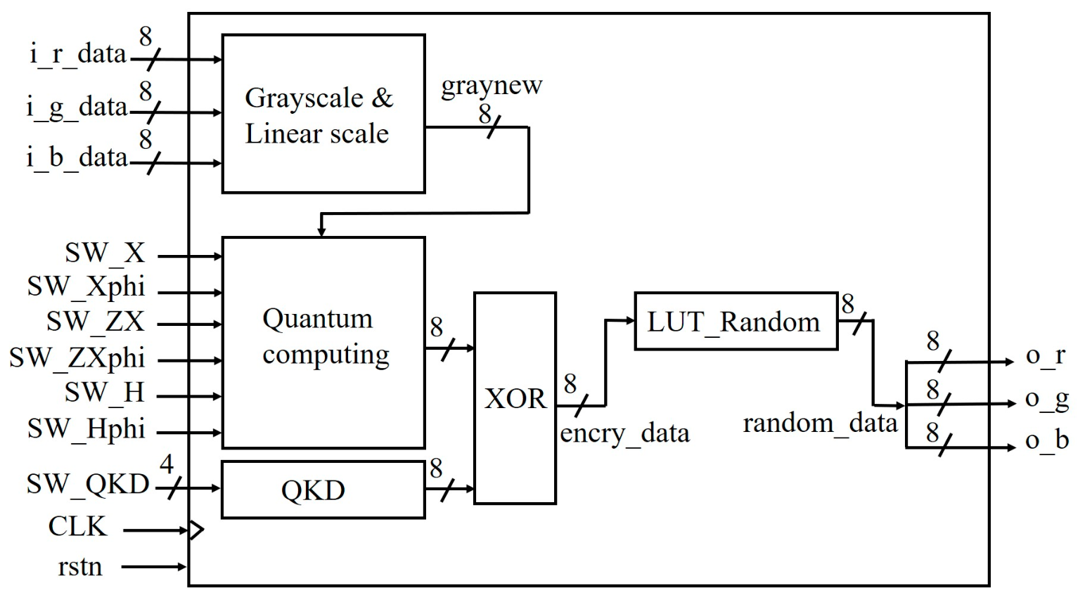
Next, we discuss the circuit design approach, as shown in
Figure 11. The grayscale and linear compression processing of the image signals, including i_r, i_g, and i_b, this signal is used as the input for the quantum computing module. The control inputs for various quantum gates are managed through the buttons located on the DE2-115 development board to execute the corresponding computations. The resultant signal following these computations is referred to as encry_data. In order to display the captured image on a VGA monitor, the computed signal, encry_data, is connected to the signal line of the VGA module. The o_r, o_g and o_b signals are the output signal after quantum operation. The SW_X is X gate
θ control from a switch. SW_Xphi is X gate
φ control from a switch. SW_ZX is ZX gate
θ control from a switch. SW_ZXphi is ZX gate
φ control from a switch. SW_H is H gate
θ control from a switch. SW_Hphi is H gate
φ control from a switch. encry_data is the output signal after quantum encryption. The switches on the development board are used to control quantum gate inputs. For the QKD random key design. However, due to resource constraints on the development board, only four switches (4 bits) are utilized here for random key input. After image pixels are encrypted via quantum gate operations and undergo XOR operations with the QKD random key, the encrypted signal encry_data undergoes random reordering with the random key plaintext data upon the arrival of the next rising edge clock pulse. The random key plaintext is implemented through an FPGA design utilizing a lookup table (LUT). LUT_Random module deals with the encry_data for random pixel permutation.
The LUT design for the random key text is as shown in
Table A2.
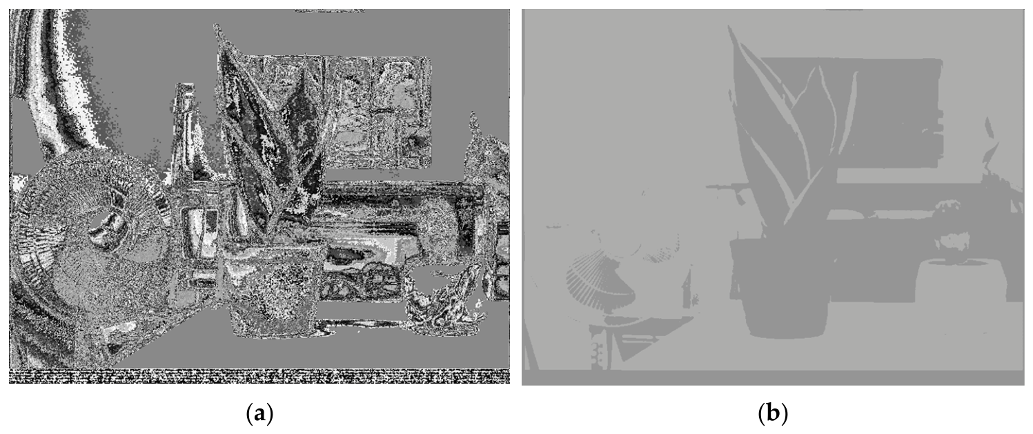
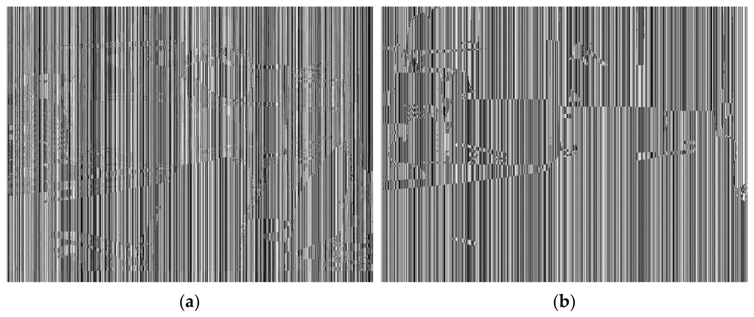
Figure 12 displays the encrypted
θ and
φ results after applying Hadamard gates to the photographed plant image with Algorithm 1. In circuit design, the inclusion of XOR operations with the QKD random key enhances security, achieving a secondary encryption effect. Even if the random key text (.txt) file is stolen, hackers cannot easily decrypt the image data because the QKD random key provides additional security protection.
3.4.2. XOR Encryption and Decryption Circuit Combining Quantum Gate Operations and Quantum Key Distribution
This section builds upon the preceding section’s theme by exploring the design of image encryption circuits in greater detail. In the preceding subsection, the integration of QKD was proposed to enhance the security of image encryption. However, as demonstrated in
Figure 12, the preliminary numerical processing applied to image pixel values 0 and 180 in the random key text data—intended to approximate their values to conceal the Hadamard gate
φ angular component image features—has unintended consequences. However, the incorporation of the XOR operation with the QKD key in the circuit results in the accentuated presentation of specific characteristics within the Hadamard gate
φ-angle component image. Consequently, the message conveyed by the original image can be inferred through either guesswork or observation.
Therefore, in contrast to the preceding subsection, with a view to achieving the objective of image encryption, the Python programming language was utilized to generate a set of random numbers ranging from 0 to 239, with a size of 800 × 1 in our random number design. Subsequently, the random key data is combined with the QKD BB84-generated random key, after which an XOR operation is applied to the image pixels that have been processed through quantum gates. Finally, another XOR operation is executed with the BB84 random key.
In the random number design, the numerical range is set from 0 to 240. This is attributable to the resource constraints of the development board, which has a maximum of four buttons designated for key input in the QKD random key design. Given that image pixel values range from 0 to 255, it is necessary to constrain the random number range to prevent it from exceeding this limit. Given that the dimensions of the captured image are 800 × 600, the size of the random number array is set to 800. Random key text data Max value is equal to (Image pixel Max value − QKD key Max value), for example 255 − 15 = 240. The encryption procedure is summarized in Algorithm 2.
| Algorithm 2. Image encryption with XOR combining quantum gate operations and quantum key distribution |
1: Input: RGB image P, QKD encryption key KQKD, quantum gate G, random key text value [H_count]
2: for angle in (θ, φ) do
3: Initialize the angle to 0 for φ
4: for each image pixel P(i) do
5: Convert P(i) into a grayscale image ccording to Equation (7)
6: Initialize the angle according to Equation (8) for θ
7: Apply quantum gate operation encryption according to the rules in Table 1 to get Q(i)
8: Read the random key text data value [H_count]
9: Adding the QKD key and random key text: R(i) = QKD_key + value [H_count]
10: Perform the first XOR encryption: XOR_data(i) = Q(i) ⊕ R(i)
11: Perform the second XOR encryption using the QKD key: C(i) = XOR_data(i) ⊕ KQKD
12: Increment H_count by 1
13: end for
14: Store the encrypted image C at the corresponding address on the SD card
15: end for
16: Output encrypted θ image and encrypted φ image |
Figure 13 presents a circuit flowchart illustrating the process of XOR encryption/decryption, which integrates quantum gate operations with quantum key distribution (BB84).
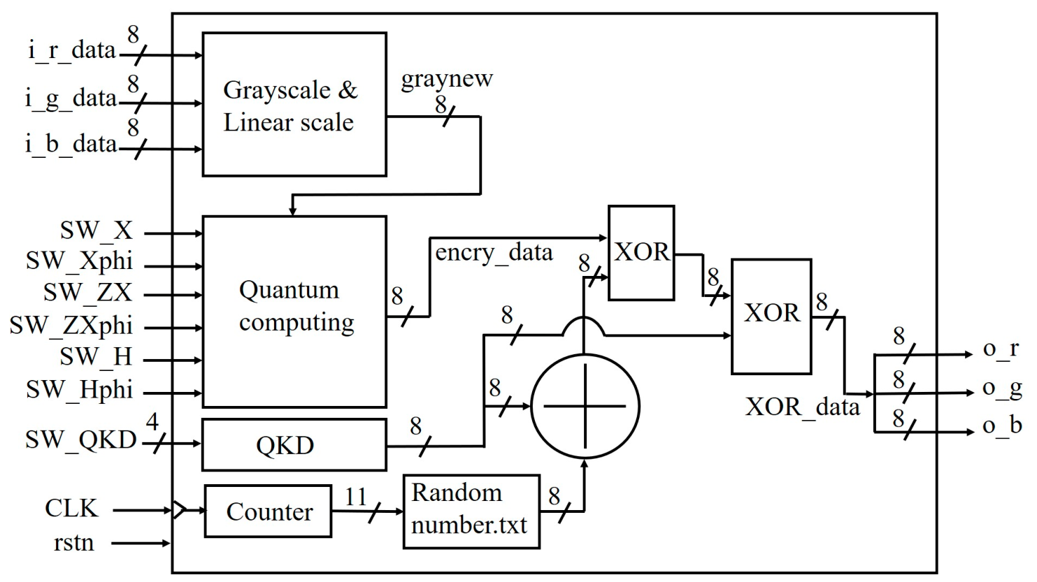
Within the encryption circuit as shown in
Figure 14, a full-color image captured by Alice using a camera undergoes grayscale conversion and linear compression processing on the development board. At the same time, she can control quantum gate operations and the QKD key via switch inputs to encrypt the image. In the decryption circuit, Alice can transmit the logic gate information to Bob and utilize quantum key distribution to send the random key message. Next, via a verified classical channel, Alice transmits the encrypted ciphertext image and the random key text data to Bob. Subsequently, Bob can use a computer to read the ciphertext image and the random key text. He then performs an XOR operation between the ciphertext image and the received QKD random key. He then conducts another XOR operation between the QKD random key and the random key text data. This process produces the pixels of the image before the XOR operations are applied. Finally, Bob can decrypt the image using reversible logic gate operations.
As shown in
Figure 14, the circuit design uses buttons on the development board to control quantum gate operations and QKD random key input, in a similar way to the previous design. XOR_data is the output signal after XOR operation. A counter is designed within the circuit to control the reading of the random key text data. When the clock produces a rising edge, the counter increments by 1; upon reaching 1056, it resets to zero and begins counting again. As previously described, the signal “encry_data”, which has been processed by quantum operations, undergoes an XOR operation with the signal obtained by adding the QKD random key “QKD_key” to the random key text data “value [H_count]”. It then undergoes another XOR operation with the QKD random key signal, QKD_key is the QKD quantum key output signal. This process achieves dual encryption of the image, ensuring security while concealing its features.
Figure 15 shows the encrypted
θ and
φ results after applying Hadamard gates to the photographed laboratory image with Algorithm 2.
3.5. Store Images to a SD Card
The following section will explore how the encrypted image signals can be stored as an image and saved onto an SD card, focusing on the concrete steps of signal processing, methods for verifying data integrity, and potential challenges in practical applications. These discussions provide detailed design methodologies and theoretical foundations for the implementation of the overall system.
3.5.1. FIFO Controller for SD Card Writing
FIFO (First in First out) is a data buffer that operates according to the principle of the same name. After performing quantum gate encryption via the control buttons, the image is stored on an SD card for subsequent decryption. However, an 800 × 600 image contains 3,840,000 bits per frame, as calculated using Equation (10). In this study, SPI mode is employed for data transfer on the SD card [
36,
37]. However, the maximum transfer speed in SPI mode is limited to 25 MHz, whereas the SDRAM clock frequency operates at 100 MHz. Therefore, a FIFO must be designed to buffer the data and facilitate the SD card’s write operations.
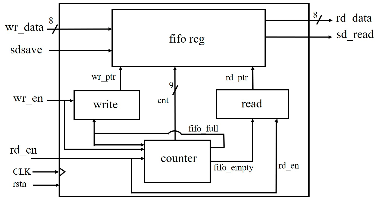
The width of a FIFO is defined as the number of data bits processed in a single read or write operation. The depth of a FIFO is indicative of the quantity of N-bit data items it is capable of storing. The FIFO designed in this study is a synchronous FIFO with a width of 8 and a depth of 512, meaning it can store 4096 bits of data at once. The circuit design is illustrated in
Figure 16. The architecture is primarily divided into four sections: the FIFO register for reading and outputting data, the write and read modules for controlling the read/write pointers, and the counter for tracking the number of data items within the FIFO. In this instance, the actuation of the button on the development board serves as the trigger for the initiation of data storage (sdsave). wr_en and rd_en is write and read enable, respectively. wr_data is the data to FIFO, rd_data is the data from FIFO to SD card. sd_read is the signal indicating start of write and counter (cnt) value. wr_ptr is pointer register for wrting and rd_ptr is pointer register for reading. fifo reg is FIFO register. fifo_full is FIFO full flag. fifo_empty is FIFO empty flag. cnt is a counter output.
3.5.2. BMP Write Controller
BMP (Bitmap) files represent one of the most prevalent image formats in Windows systems, characterized by their ability to preserve the integrity of image data. In the present study, encrypted data is stored as a bmp image file and saved to an SD card. The structure of a BMP file is characterized by four distinct sections: the BMP header, the BMP data header, the palette, and the image data. In the study, an 800 × 600 BMP image was first saved to an SD card, and its sector address was obtained. In circuit design, when the storage switch is toggled, the image data is overwritten into the designated sector for storage.
In the domain of circuit design, a state machine approach is employed to facilitate communication with the SD card.
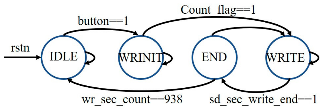
Figure 17 presents a flowchart illustrating the state machine of the BMP module. The model under consideration comprises four states and their transitions. The states are as follows:
IDLE: This is the initial state, indicating that the system is in an idle condition.
WRINIT: After receiving the “button” signal from the IDLE state, the system transitions to this state, representing the initialization of the write operation.
WRITE: Upon receiving the “Count_flag” signal from the WRINIT state, the system enters this state, indicating that the write operation is in progress.
END: After receiving the “sd_sec_write_end = 1” signal from the WRITE state, the system transitions to this state, representing the completion of the write operation. When the “wr_sec_count” signal reaches 938, the system returns to the IDLE state.
Figure 17.
State machine flow diagram of the BMP module.
Figure 17.
State machine flow diagram of the BMP module.
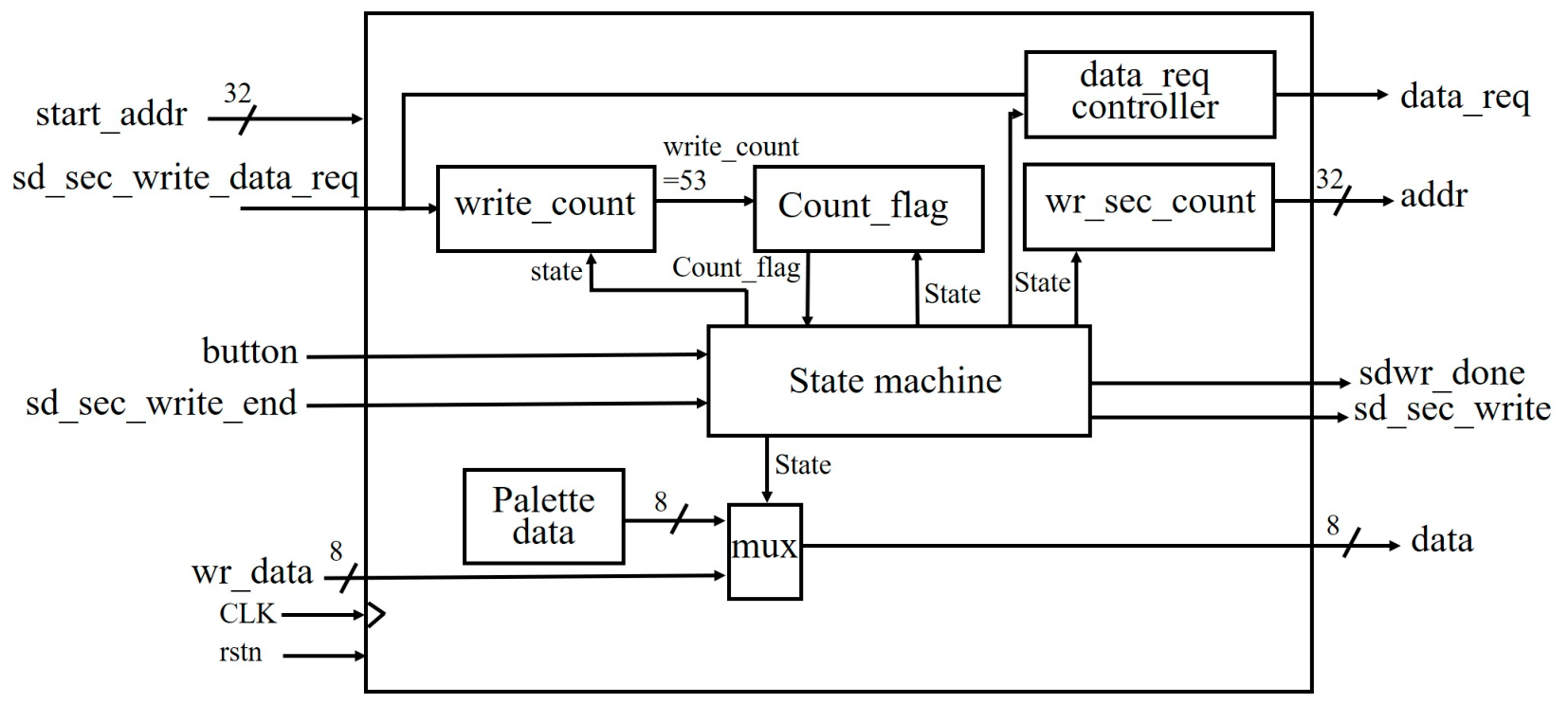
The button signal is connected to the sd_read signal from the previous section’s FIFO module to determine whether data writing should commence. Before the storage of image data, 53 palette entries are allocated to the initial sector. Consequently, within the context of circuit design, the 53 palette entries are initially defined during the process of initialization, with the subsequent addition of image data. The circuit design is illustrated in
Figure 18. When the write_count for the BMP image data reaches 53, the Count_flag signal is set to 1, causing the state machine to enter the WRITE state. Subsequently, the process commences the writing of image data and concomitantly updates the value of the Count_flag signal. Upon reaching its maximum capacity, the SD card’s current sector initiates the transmission of the sd_sec_write_end signal. This, in turn, prompts the state machine to transition to the END state and facilitate the update of the sector address, thereby enabling the continuation of the writing process. This process is repeated iteratively until all images have been fully written. Given that the stored image size is 800 × 600 pixels and each memory card sector have a storage capacity of 512 bytes, the total number of sectors required is 938. The detailed calculations are presented in Equation (11). Upon attaining a value of 938 by the counter responsible for monitoring the current sector position, the state machine transitions to the initial state (IDLE) in preparation for the storage of a new image. sd_sec_write_data_req is the SD card write request signal. start_addr is the initial SD card sector address. sd_sec_write_end is the SD card write completion signal. write_data is the data to write, data_reg is the flag for new data request. addr is the SD card sector address for writing. sdwr_done is the flag for all data write finished. sd_sec_write is the signal for SD card sector write. data is the SD card write data. write_count is the BMP image data counter. Conut_flag is the state machine status flag. wr_sec_count is the SD card sector address counter.
3.5.3. SD Card Controller
In this study, encrypted BMP images are stored on an SD card for subsequent decryption operations. The SD card operates in two modes: SDIO mode and SPI mode. The present paper employs SPI mode as the data transfer protocol for the SD card. Prior to the execution of read/write operations, it is imperative that the SD card undergoes initialization. The host issues commands to the SD card in accordance with a predetermined 48-bit format, which is transmitted in a continuous manner via the CMD signal line. The overall process commences with the querying of the SD card’s version number using the CMD8 command. The subsequent step involves the transmission of the CMD55 command, the purpose of which is to ascertain the version of the SD card, whether it is version 1.0 or 2.0. Upon completion of the confirmation process, the system transitions into the standard read/write operation procedure, thereby facilitating data access operations on the SD card.
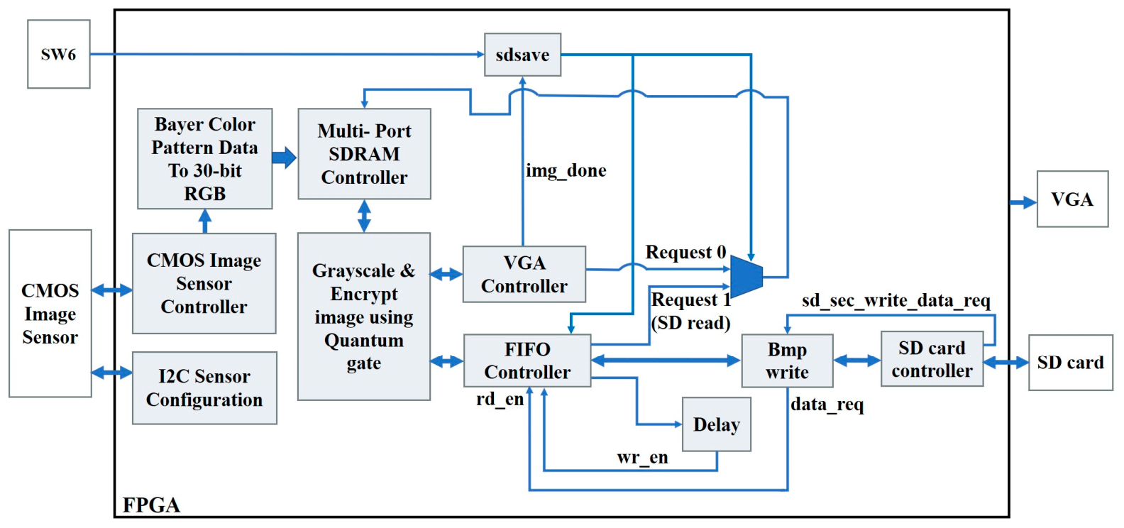
In this study, the switch SW6 on the FPGA board is utilized to trigger the SD card image storage process. Measures must be implemented to prevent image output from commencing at an erroneous pixel array during the storage process, given the elevated clock speed of SDRAM and the synchronous output of images via VGA cable to the LCD screen. Consequently, in the circuit design, the official open-source VGA controller program was modified to output an “img_done” signal when the image pixel count returns to the first image pixel. Concurrently, the initiation of the image storage process is contingent upon the triggering of SW6. The detailed data flow signal transmission is illustrated in
Figure 19. The SD controller initiates a data request signal, thereby enabling the host to write data. It is evident that, to process retrieved data from SDRAM, this must first undergo processing through the ‘Grayscale & Encrypt image using the Quantum gate’ module. This process necessitates the incorporation of a one-clock delay into the FIFO controller’s write enable signal. The configuration under consideration is designed to ensure that image data is processed and stored at the correct time, thus preventing any conflicts between synchronous output and storage operations.
4. Results
This section presents and discusses the experimental results obtained in this study. It will provide a detailed analysis of the findings, evaluating and comparing their performance. For encryption, we captured an 800 × 600-pixel real-time image using the TRDB-D5M camera in the study. We photographed a laboratory, plants, and figurines. We then designed various quantum gate inputs using switches on the FPGA development board to encrypt the images and store them on an SD card. To decrypt the images, we used a computer to read the image data from the SD card and performed decryption operations leveraging the reversible nature of quantum gate computations. The following sections will discuss these results in further detail, examining their effectiveness and potential applications.
4.1. Experimental Results of Encryption and Decryption Circuit Combining Quantum Gate Operations and Quantum Key Distribution (BB84)
As delineated in the preceding section, we utilize quantum gate operations to encrypt images. However, experimental findings suggest that image features remain readily identifiable. Moreover, the subsequent analysis of the images reveals an absence of sufficient randomness, rendering them vulnerable to decryption. To enhance the concealment of image features and prevent malicious actors from intercepting random number sequence text (.txt) files transmitted over classical channels, we integrated concepts from quantum key distribution (BB84) to design the encryption circuit. The security of quantum key distribution is leveraged to ensure the integrity of the images.
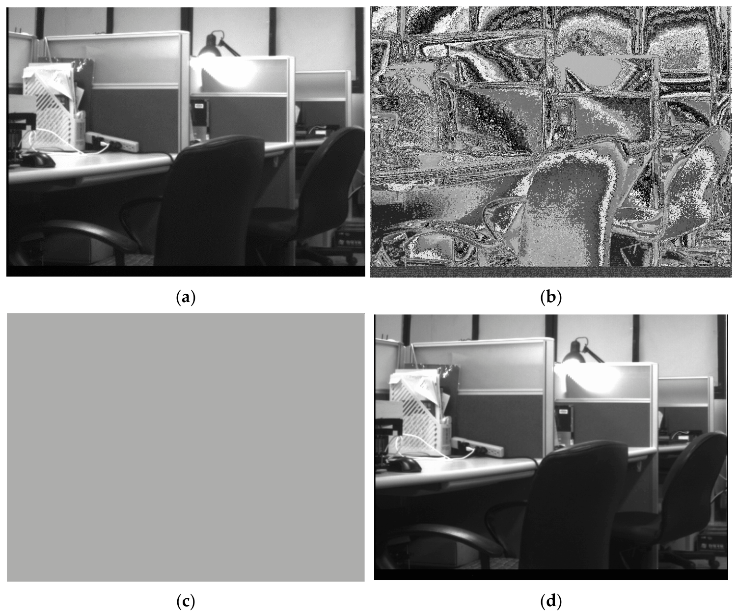
In the circuit design of this section, we first perform an XOR operation between the image pixels processed by quantum gates and the BB84 random key. Subsequently, the image data undergoes random sorting to scramble the original pixel values. As illustrated in
Figure 20a, the grayscale conversion of the captured laboratory full-color image is demonstrated. The encrypted images
θ and
φ, processed using Pauli-Z gates and Pauli-X gates, are shown in
Figure 20b and
Figure 20c, respectively. The encrypted image and randomly sorted text were subsequently processed by a computer. The Python Dictionary function was employed to retrieve the original pixel values before randomization. The encrypted image was subsequently decrypted through a series of BB84 random key XOR operations and reversible logic gate operations. The decryption result is illustrated in
Figure 20d.
In image encryption systems, entropy is a pivotal metric for quantifying the randomness of image data. As the entropy increases, the encrypted image becomes more random, thus leading to a more challenging decryption process. In the domain of digital image processing, the entropy of an image is determined by the probability of occurrence for each pixel’s grayscale value. Higher entropy is indicative of greater information content within the image, suggesting a more complex or irregular image. A detailed analysis was conducted of the randomness of the encrypted images θ and φ, to evaluate the effectiveness of the encryption algorithm by calculating the randomness values of different encrypted images. In order to assess the distortion of decrypted images, PSNR values are utilized for analysis. Peak Signal-to-Noise Ratio (PSNR) is a common metric used to evaluate the quality of images or video after compression. The objective of this process is to quantify the discrepancy between the original signal and the noisy signal, thereby reflecting the degree of similarity between the compressed image or video and its original version. A higher PSNR value indicates that the processed image is closer to the original image and thus of higher quality. Typically, a PSNR above 30 dB is indicative of good image quality, at which point the human eye struggles to discern differences between the processed image and the original.
From the experimental results above, it can be observed that while some degree of concealment is maintained in the image features and the addition of the QKD random key improves image security, performing the XOR operation on image pixels with a fixed number tends to amplify the edges of image features, making them easier to infer. In terms of evaluating image encryption security,
Table 2 presents the randomness metrics for the encrypted images
θ and
φ. However, the data indicate that, although the entropy value for the
θ encrypted image is within an acceptable range, the entropy value for the
φ encrypted image could still be improved. For image quality assessment, we analyze the PSNR values as presented in
Table 3. Experimental data indicate that, since the circuit also uses a lookup-table-based design for value mapping, significant image distortion remains. The next section will continue to examine image encryption enhancement methods targeting image quality.
4.2. Experimental Results of XOR Encryption and Decryption Circuit Combining Quantum Gate Operations and Quantum Key Distribution (BB84)
This section builds on the previous one by examining the security of encrypted circuit designs in greater detail. Previously, we combined quantum gate operations with the BB84 quantum key distribution protocol to create encryption and decryption circuits intended to improve image data security. However, our experiments showed that this approach unexpectedly enhances edge features in images. Additionally, when creating random number steganographic texts, simply scrambling the original data into a different sequence was insufficient to hide image features. Therefore, in this section, we use BB84-generated random keys to protect images better and refine our data design methodology. Instead of an FPGA-based lookup table (LUT) design for random sorting, we read random number text data from TXT files and apply row-by-row XOR operations to each image value. This increases the randomness of the encrypted data. Due to spatial resource limitations, the designs in this section only process data sets of size 800 × 1. These improvements aim to enhance the security of image encryption.
The study also used Pauli-X gates, Pauli-H gates, and Pauli-Z gates in combination with Pauli-X gates for experimentation.
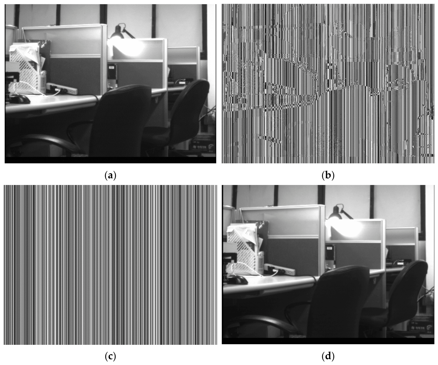
Figure 21a shows the results of converting laboratory-captured full-color images to grayscale. The encrypted images
θ and
φ, obtained using Pauli-Z gates and Pauli-X gates, are illustrated in
Figure 21b,c. Finally, the encrypted images and the random number key text were read by a computer. Decryption was performed using the BB84 random key, XOR operations on the key text, and reversible logic gate operations. The decryption result is presented in
Figure 21d.
The experimental results above demonstrate a significant improvement in concealing image features. Additionally, integrating the BB84 random key effectively enhances image security. To assess the security of the image encryption, we used randomness metrics to analyze the encrypted images
θ and
φ, as shown in
Table 4. The experimental data reveal that both encrypted images exhibit randomness values close to the maximum of 8. This indicates that the XOR encryption/decryption circuit design, which combines quantum gate operations with quantum key distribution, effectively improves image security. As for image quality, the PSNR data in
Table 5 show values consistently above 30 dB, indicating that image quality is well preserved before and after encryption. The human eye finds it difficult to distinguish between the processed and original images. Overall, these results demonstrate that our design successfully enhances image encryption and addresses security challenges.
5. Discussion and Future Works
This section continues the discussion from the previous section by examining the outcomes of different design approaches.
Table 6 presents the average entropy data for three images subjected to three quantum gate operations across three circuit designs. Similarly,
Table 7 provides the average PSNR data for these images after three quantum gate operations across the same circuit designs.
Ref. [
26] represented an encryption circuit based solely on quantum gate operations; Algorithm 1 incorporates both quantum gate operations and quantum key distribution; and Algorithm 2 denotes an XOR encryption/decryption circuit that also combines quantum gate operations with quantum key distribution. The experimental results in
Table 6 reveal a significant security vulnerability of the gate-only encryption approach (Algorithm 1). Specifically, the low entropy values in the phi component suggest that image features are not sufficiently randomized. This lack of diffusion means recognizable patterns may persist in the encrypted component, allowing an adversary to potentially reconstruct the original image through statistical analysis. These findings demonstrate that, although quantum gate operations provide a sophisticated, quantum-inspired logic layer, they are insufficient as a standalone encryption solution. To address this issue, the proposed Algorithm (XOR/BB84 integration) scheme was developed. Our analysis confirms that introducing random keys via the BB84 protocol, followed by XOR diffusion, is indispensable for practical security, not merely an optional enhancement. The evolution from Algorithm 1 to Algorithm 2 ensures that both the
θ and the
φ components reach high-entropy states, effectively neutralizing any traceable image characteristics. Our research achieves significant advancements and distinctiveness in quantum image encryption and decryption. Firstly, we accomplished real-time encryption and decryption of grayscale images. By measuring image randomness using entropy, we achieved results close to the maximum value of 8. While this is comparable to [
22], our approach yields a higher image quality assessment, with a PSNR exceeding 30 dB, indicating marked improvement. Secondly, our method demonstrates flexibility and efficiency in quantum bit usage. In contrast to the 24 entangled qubits used in [
21] and 8 in [
22], our system requires only one qubit for implementation. The quantum state is processed through its state vector, rather than being measured, to derive the theta and phi values. This not only reduces system complexity but also enhances the feasibility and cost-effectiveness of practical applications.
Although the angular operations within the quantum gates are linear, the underlying quantum state operates in the complex domain. Consequently, even a slight variation in
θ or
φ triggers a complete shift in the state vector. Coupled with the highly nonlinear nature of XOR operations and BB84 random keys, the system effectively thwarts differential attacks. Furthermore, although the pixel values (0–255) are compressed into the range of the Bloch sphere (0–180°), experimental results confirm that the PSNR remains above 30 dB. These results prove that the reconstruction error is minimal and that the essential features of the original image are accurately preserved. Furthermore, the quantum image encryption and decryption algorithm we propose goes beyond static image processing and can be applied to real-time image encryption systems. This allows for real-time encryption and decryption of live video streams—a capability not achieved in [
21] or [
22].
In summary, the proposed research makes significant breakthroughs in quantum image encryption and decryption by optimizing image quality, improving quantum bit utilization, and enabling real-time practical applications. This work serves as a valuable reference and inspiration for future research in the field.
Regarding hardware resource utilization, this circuit incorporates quantum gate operations and the QKD key distribution protocol. The report shows a logic element utilization rate of only 11% and memory utilization of 17%. This high efficiency is primarily attributed to the proposed LUT-based design for image processing as detailed in
Table 8. Furthermore, the proposed FPGA architecture achieved a maximum operating frequency (fmax) of 105.16 MHz for the encryption module as shown
Figure 14. Thus, we proposed a quantum-inspired architecture for quantum gate operations based on the Bloch sphere concept. By transforming the conventional quantum operators—which typically require resource-intensive trigonometric functions (
) [
38,
39]—into linear angular additions and subtractions, we significantly reduced the computational overhead and hardware cost. This optimization allows for a more streamlined hardware implementation. Experimental results indicate that the algorithm used in Ref. [
26] utilized the fewest logic elements, while the proposed Algorithm 1 and Algorithm 2 require significantly more resources due to their more complex numerical operations.
In contrast to conventional AES-128 encryption, which may require substantial logic slices and complex partitioning to achieve high-speed, lightweight performance as noted in [
40], its security remains fundamentally dependent on mathematical complexity, making it vulnerable to future large-scale quantum threats. The proposed design in this work operates at 40 MHz with an 8-bit grayscale output in order to display image to VGA, resulting in a throughput of approximately 320 Mbps. Timing analysis results show that the proposed FPGA implementation operates at a maximum frequency of 105.16 MHz. With one 8-bit grayscale pixel processed per clock cycle, the achievable throughput is approximately 841.28 Mbps. The proposed design achieves a significantly lower latency of only 1 clock cycle, compared to 11 cycles in [
40], making it suitable for real-time streaming applications. However, the current implementation of the proposed system is limited to grayscale image processing. Expanding the architecture to support full-color (RGB) imagery and multi-channel data representation remains a key objective for future research.
6. Conclusions
This paper proposes a novel image encryption method and achieves real-time image encryption using an FPGA. Images are captured with a CMOS module, and encryption is performed on an FPGA development board, which executes quantum gate operations and uses random key input controlled by onboard switches. The integrated XOR encryption/decryption circuit design combines quantum gate operations and random key distribution, substantially improving image concealment and security. Entropy analysis yields values near the maximum of 8, indicating that the encrypted image data demonstrates high randomness and resists decryption attacks. The use of multiple quantum logic gates increases encryption complexity, though the resulting increase in decryption time remains acceptable. The decryption circuit leverages the reversible characteristics of quantum computation, enabling image restoration through reversible quantum gates. Experimental results show the proposed method effectively conceals image features, confirming the security and performance of the designed image encryption/decryption system. Utilizing an FPGA greatly accelerates the encryption process. In image quality assessments, peak signal-to-noise ratio values above 30 dB indicate the system effectively prevents image distortion. While the current study has preliminarily validated the system’s security through entropy and PSNR metrics, more rigorous evaluations are planned for future work. Specifically, we intend to incorporate a broader range of quantitative analyses, including adjacent pixel correlation, histogram uniformity, and sensitivity metrics such as NPCR and UACI. To address existing hardware constraints on key length, future research will focus on optimizing the key generation and input mechanisms. These efforts will include a comprehensive assessment of key space and resistance against brute-force attacks to ensure the system’s robust security in practical applications.
This achievement demonstrates the potential of quantum technology in image encryption and serves as a reference for future applications. Further research can optimize quantum logic gate operations to improve encryption efficiency and explore additional uses of quantum technology in image information security.