
Essay

Electrical Modeling and Structural Parameter Optimization of Shielded Quad-Axis Differential Through-Silicon Vias


School of Electronic Science and Engineering, South China Normal University, Foshan 528225, China
*
Author to whom correspondence should be addressed.
Electronics 2026, 15(10), 2186; https://doi.org/10.3390/electronics15102186
Submission received: 10 February 2026 / Revised: 16 April 2026 / Accepted: 17 April 2026 / Published: 19 May 2026
(This article belongs to the Section Circuit and Signal Processing)

Abstract

This paper proposes a novel shielded quad-axis differential through-silicon via (SQDTSV) structure. Initially, the parasitic parameters are extracted, and the applicability of the equivalent circuit model and analytical formulas is verified through a combined approach of HFSS simulations and MATLAB computations, leading to the establishment of an accurate equivalent circuit model. Subsequently, based on the single-variable principle, a systematic investigation is conducted to analyze the influence of multidimensional physical parameters—such as via height, signal conductor radius, and dielectric isolation thickness—on the transmission characteristics. An optimization model is then constructed via parameter sensitivity analysis. Simulation results demonstrate that, within the 0–100 GHz frequency band, the optimized SQDTSV structure has significantly improved performance across the entire frequency range. The differential-mode return loss has increased by more than 6.98 dB in the 50–100 GHz high-frequency band after optimization. In terms of transmission efficiency, the insertion loss in the low-frequency range (0–10 GHz) has decreased by more than 27%, and in the high-frequency range (10–100 GHz), it has decreased by over 11%, thereby significantly improving overall transmission performance.

1. Introduction

Through-silicon vias (TSVs), serving as a critical component for vertical interconnections in three-dimensional integrated circuits, play a pivotal role in enhancing integration density and system performance. Their electrical characteristics directly impact the signal integrity, power consumption, and reliability of the overall system. Conventional single-ended TSV configurations face significant challenges such as signal crosstalk, electromagnetic leakage, and increased power dissipation in high-frequency and high-density interconnect scenarios [1]. To address these limitations, coaxial TSV structures—featuring a central signal conductor enclosed by an outer grounded shielding layer—have been developed. By confining the electromagnetic field entirely within the dielectric region between the inner and outer conductors, coaxial TSVs exhibit superior performance, characterized by low insertion loss, enhanced electromagnetic shielding, and minimal crosstalk, making them particularly suitable for high-frequency and high-noise environments [2]. The realization of coaxial ring-shaped TSVs can be achieved through DRIE (Deep Reactive Ion Etching) [3,4]. DRIE has the advantages of fast etching speed and a high aspect ratio of etched grooves, and has become the most widely used etching technology in the current TSV process. By controlling the experimental conditions in the electroplating process, ring-shaped TSVs with central hollowing can be made in the cylindrical grooves. The current aspect ratio of TSVs has reached 1:20.
On the other hand, at high-speed I/O interfaces, differential signaling technology serves as a mainstream solution for ensuring signal integrity. Correspondingly, the Ground–Signal–Signal–Ground (GSSG)-type differential TSV structure has been extensively studied and widely adopted. By leveraging its common-mode rejection capability, this configuration significantly enhances anti-interference performance and has become a common implementation form for high-speed differential transmission channels [5]. However, in high-density TSV arrays, the random states of adjacent through-silicon vias make GSSG structures susceptible to differential-mode noise. This issue particularly degrades the quality of differential signals during high-frequency signal transmission, seriously impairing transmission performance.
Leveraging the advantageous characteristics of coaxial TSVs, such as low loss and high noise immunity, researchers have endeavored to model and analyze these structures using partial element equivalent circuit models [6] and broadband impedance models [7]. Building on this foundation, novel composite configurations such as the Shielded Differential Through-Silicon Vias (SDTSVs) [8], have been proposed, which integrate the robustness of differential signaling with the superior isolation properties of coaxial shielding. As shown in Table 1, The SDTSVs combine the advantages of both coaxial and GSSG TSVs.

2. Parasitic Parameter Extraction and Equivalent Circuit Modeling of Shielded Quad-Axis Differential Through-Silicon via (SQDTSV) Structure

The 3D and cross-sectional views of the shielded quad-axis differential through-silicon via (SQDTSV) structure are shown in Figure 1, where the inner four TSVs are used to transmit differential signals, and the outer metal layer serves as the shielding layer and return path. In this figure, r i (i = 1–6) is the radius of the SQDTSVs, ρ is the signal line pitch, and h is the height. The relative permittivity of Si ( ε S i ) and SiO2 ( ε o x ) is 11.9 and 4, respectively. The conductivity of Si ( σ S i ) and Cu ( σ C u ) is 10 and 5.8 × 10⁷ S/m, respectively. In addition, it should be noted that the Si substrate does not apply any bias voltage, so the MOS capacitance between the Cu and Si substrate does not need to be considered [8,11].
R denotes the loop resistance, which encompasses the resistance of the signal line and its return path, and it can be expressed as [12]
R = Re Z wire + Re Z shield ,
with
Z w i r e = T I 0 T r 1 2 π r 1 σ C u I 1 T r 1 ,
Z shield = T π σ C u r 5 · I 0 T r 5 K 1 T r 4 + I 1 T r 4 K 0 T r 5 I 1 T r 5 K 1 T r 4 I 1 T r 4 K 1 T r 5 ,
with
T = ω μ 0 σ C u 1 / 2 e j π / 4 .
I 0 and I 1 represent the modified Bessel functions of the first kind, of orders zero and one, respectively; K 0 and K 1 denote the modified Bessel functions of the second kind, of orders zero and one, respectively. Similar to R , L denotes the loop inductance, which comprises the inductance of a signal conductor and that of its return path. It can be expressed as
L = L i , w i r e + L i , s h i e l d + L e ,
with
L i , w i r e = I m Z w i r e 2 π f ,
L i , s h i e l d = I m Z s h i e l d 2 π f ,
L e = μ 0 2 π l n r 4 2 ρ / 2 2 r 4 r 1 .
They represent the internal inductance and external inductance of the signal line and its return path in the shield layer, respectively. The mutual inductance between two differential signal lines is [13,14]
L m 1 = L m 1 , i + m 1 L i , wire + L i , shield ,
with
L m 1 , i = μ 0 2 π ln 2 r 4 2 + ρ / 2 2 2 r 4 ρ ,
m 1 = L m 1 , i / L e .
The coupling inductance between the two same signal lines is
L m 2 = L m 2 , e + m 2 L i , wire + L i , shield ,
where
L m 2 , e = μ 0 2 π ln r 4 2 + ρ / 2 2 r 4 ρ ,
m 1 = L m 1 , i / L e .
L m 1 , i and L m 2 , e , respectively, represent the internal coupled inductance and the external coupled inductance. m 1 and m 2 , respectively, represent the internal mutual coefficient and the external mutual coefficient. C o x 1 and C o x 2 are the oxide capacitance between [ r 1 , r 2 ] and [ r 3 , r 4 ], respectively, and can be calculated as follows:
C o x 1 = 2 π ε o x ln r 2 / r 1
C o x 2 = 2 π ε o x ln r 4 / r 3
Since the Si substrate can be treated as a uniform dielectric, the capacitance matrix can be calculated by the inductance matrix with the relation
L L m 1 L m 2 L m 1 L m 2 L L m 2 L L m 1 C S i 1 + C S i 2 + C S i 3 C S i 1 C S i 2 C S i 1 C S i 1 + C S i 2 + C S i 3 C S i 2 C S i 2 C S i 1 C S i 1 + C S i 2 + C S i 3 = μ 0 ε S i ε 0 1 0 0 0 1 0 0 0 1 ,
where
L = μ 0 2 π ln r 3 ρ / 2 2 r 3 r 2 ,
L m 1 = μ 0 2 π ln 2 r 3 2 + ρ / 2 2 2 r 3 ρ ,
L m 2 = μ 0 2 π ln r 3 2 + ρ / 2 2 r 3 ρ .
where C S i 1 , C S i 2 and C S i 3 , respectively, represent the capacitance between two different signals, the capacitance between two identical signals, and the capacitance between the signal line and the shielding layer. Solving this, we can obtain
C Si 1 = μ 0 ε Si ε 0 L L m 2 L m 1 2 L 3 + L m 1 3 + L m 2 3 3 L L m 1 L m 2 ,
C Si 2 = μ 0 ε Si ε 0 L L m 1 L m 2 2 L 3 + L m 1 3 + L m 2 3 3 L L m 1 L m 2 ,
C Si 3 = μ 0 ε Si ε 0 L 2 + L m 1 2 + L m 2 2 L L m 1 L m 1 L m 2 L L m 2 L 3 + L m 1 3 + L m 2 3 3 L L m 1 L m 2 .
Therefore, G S i 1 , G S i 2 and G S i 3 , respectively, represent the conductance between two different signals, the conductance between two identical signals, and the conductance between the signal line and the shielding layer, calculated by
G Si 1 = μ 0 σ Si L L m 2 L m 1 2 L 3 + L m 1 3 + L m 2 3 3 L L m 1 L m 2 ,
G Si 2 = μ 0 σ Si L L m 1 L m 2 2 L 3 + L m 1 3 + L m 2 3 3 L L m 1 L m 2 ,
G Si 3 = μ 0 σ Si L 2 + L m 1 2 + L m 2 2 L L m 1 L m 1 L m 2 L L m 2 L 3 + L m 1 3 + L m 2 3 3 L L m 1 L m 2 .
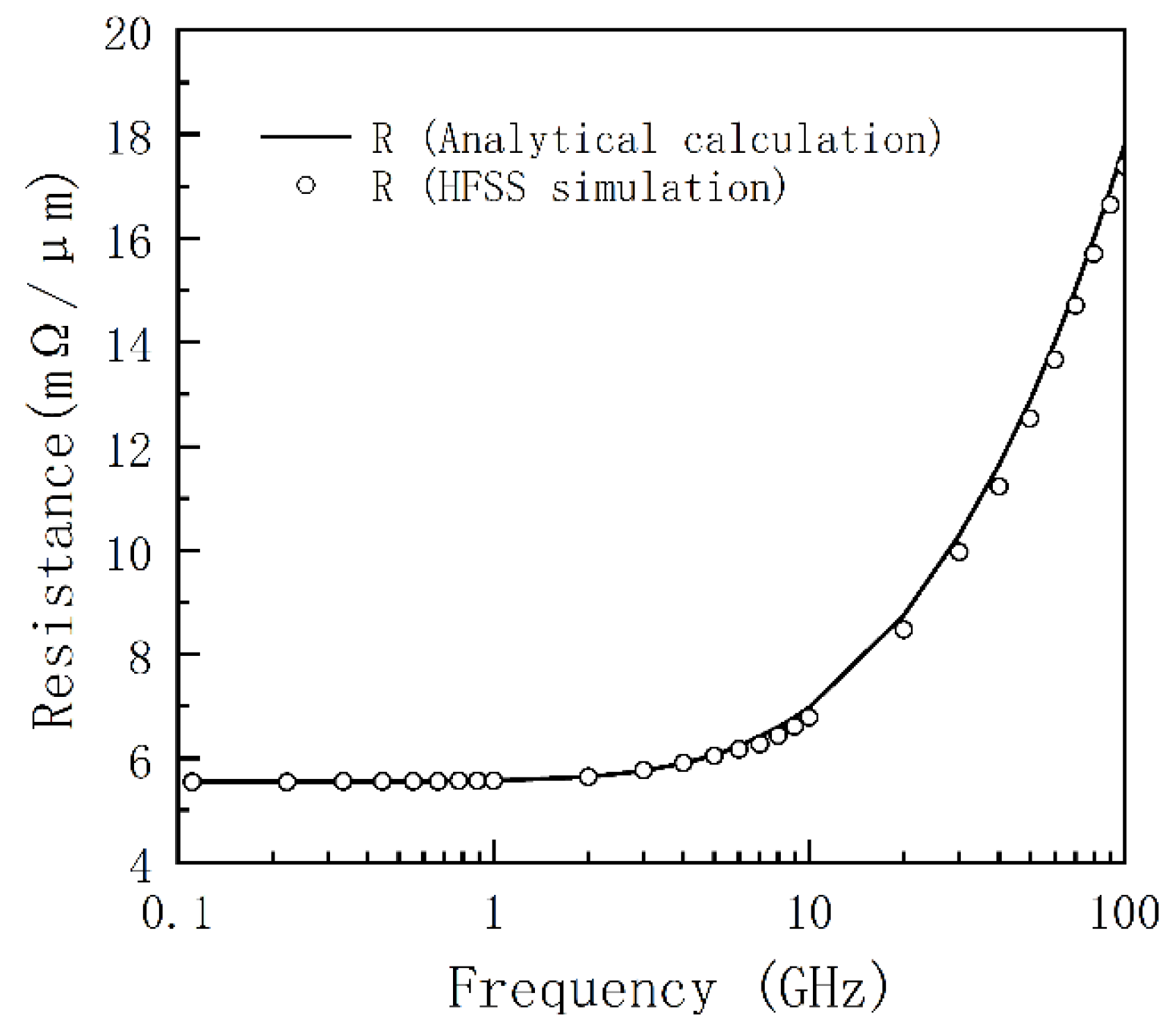
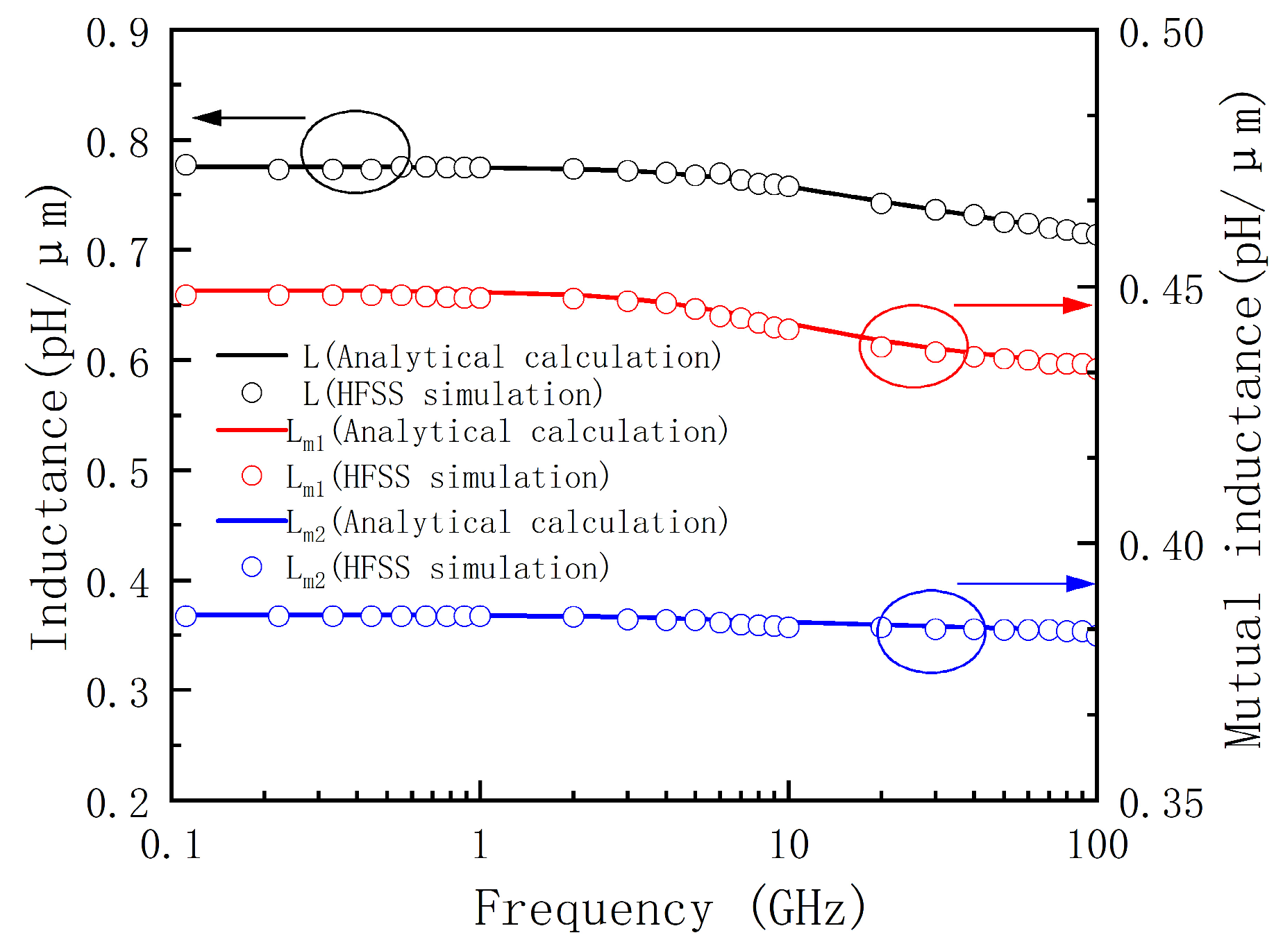
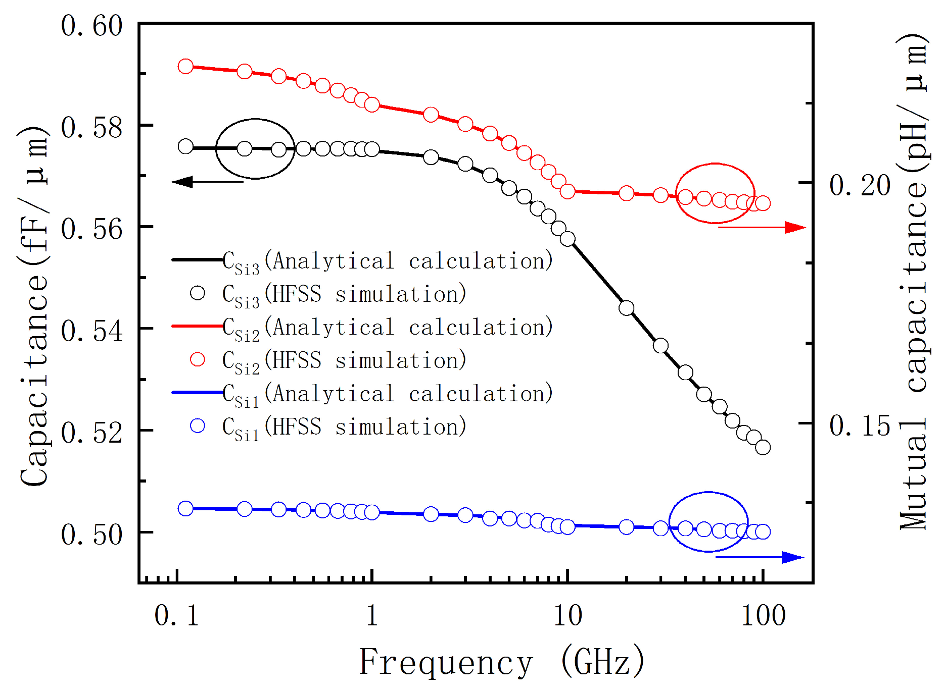
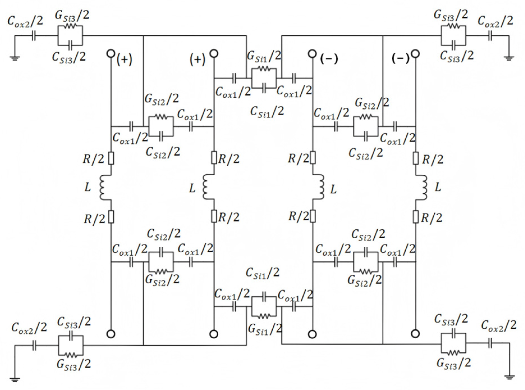
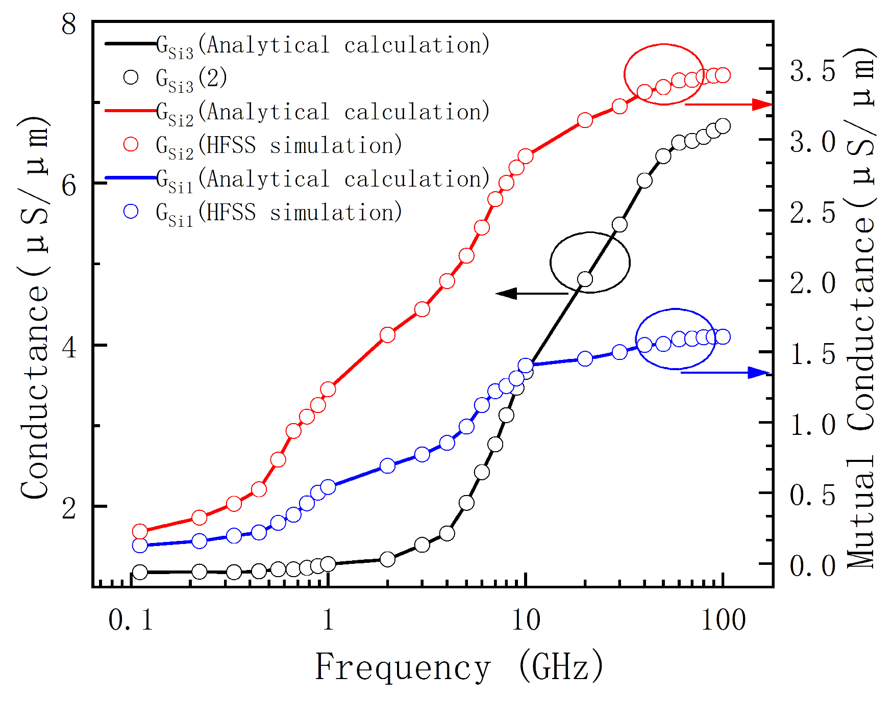
In order to verify the accuracy of the equivalent circuit model, each structural parameter of SQDTSVs was substituted into the formula for calculation in MATLAB R2024b ( r 1 = 1 μm, r 4 = 12 μm, r 5 = 13 μm, ρ = 6 μm, h = 50 μm, thickness of silicon dioxide layer (isolated layer) t o x = 0.2 μm). The physical model is simulated in HFSS (Ansys Electronics 2024 R2), the terminal drive solution mode is selected, and wave ports are defined with a radius of 13 μm, which is equal to the radius of the outer surface of the outer shell. The simultaneous shielding layer and four signal lines are defined as reference conductors and double difference pairs, respectively. The unit length values of R, L, L m 1 and L m 2 are calculated by theoretical and simulation models. As shown from Figure 2, Figure 3, Figure 4 and Figure 5, it can be seen that they are well matched in the frequency range up to 100 GHz [15,16]. Hence, the equivalent circuit diagram of the SQDTSVs structure can be derived [17], as shown in Figure 6. The ratio of the maximum error between the simulation values and the calculated values to each of them is less than 4.26%.
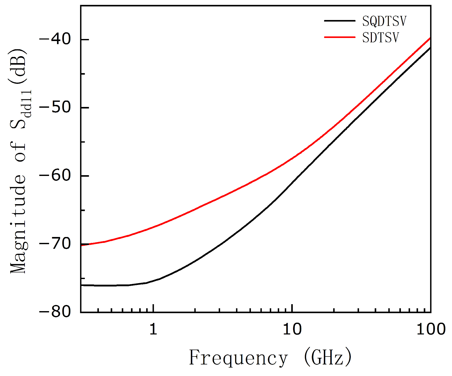
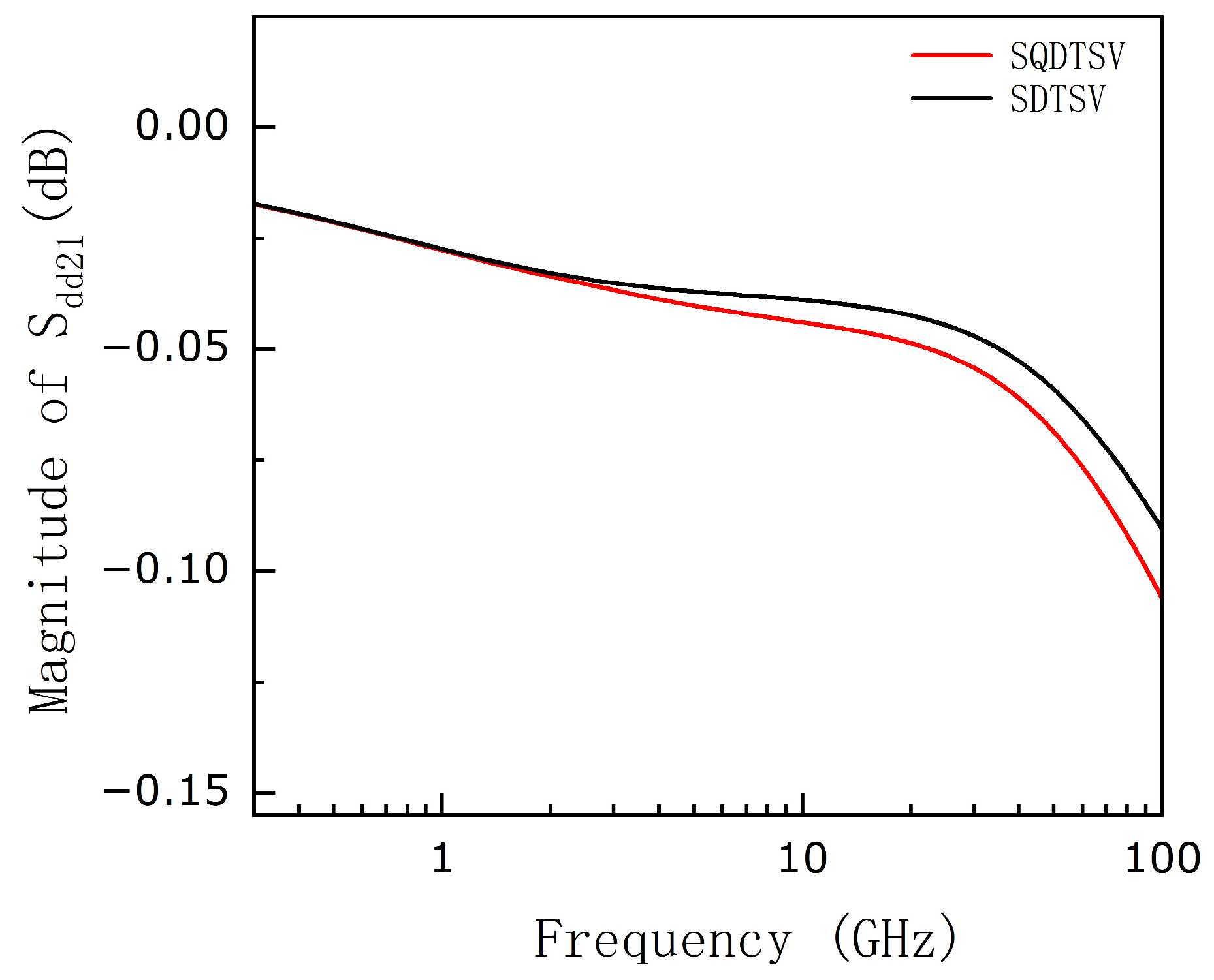
Since the equivalent circuit model of SQDTSVs has high accuracy in the frequency range up to 100 GHz, and since there is mutual capacitance and mutual conductance between the four signal lines in differential mode, although they do not exist in common mode, Figure 7 and Figure 8, respectively, compare the Sdd11 and Sdd21 of SQDTSVs and SDTSVs [8] simulated by HFSS. It can be seen that with roughly the same differential-mode insertion loss, SQDTSVs have a smaller differential-mode return loss than SDTSVs, and the difference is more obvious in the middle and low-frequency region.

3. Optimization of the Structure and Material Parameters of Shielded Quad-Axis Differential Through-Silicon Vias

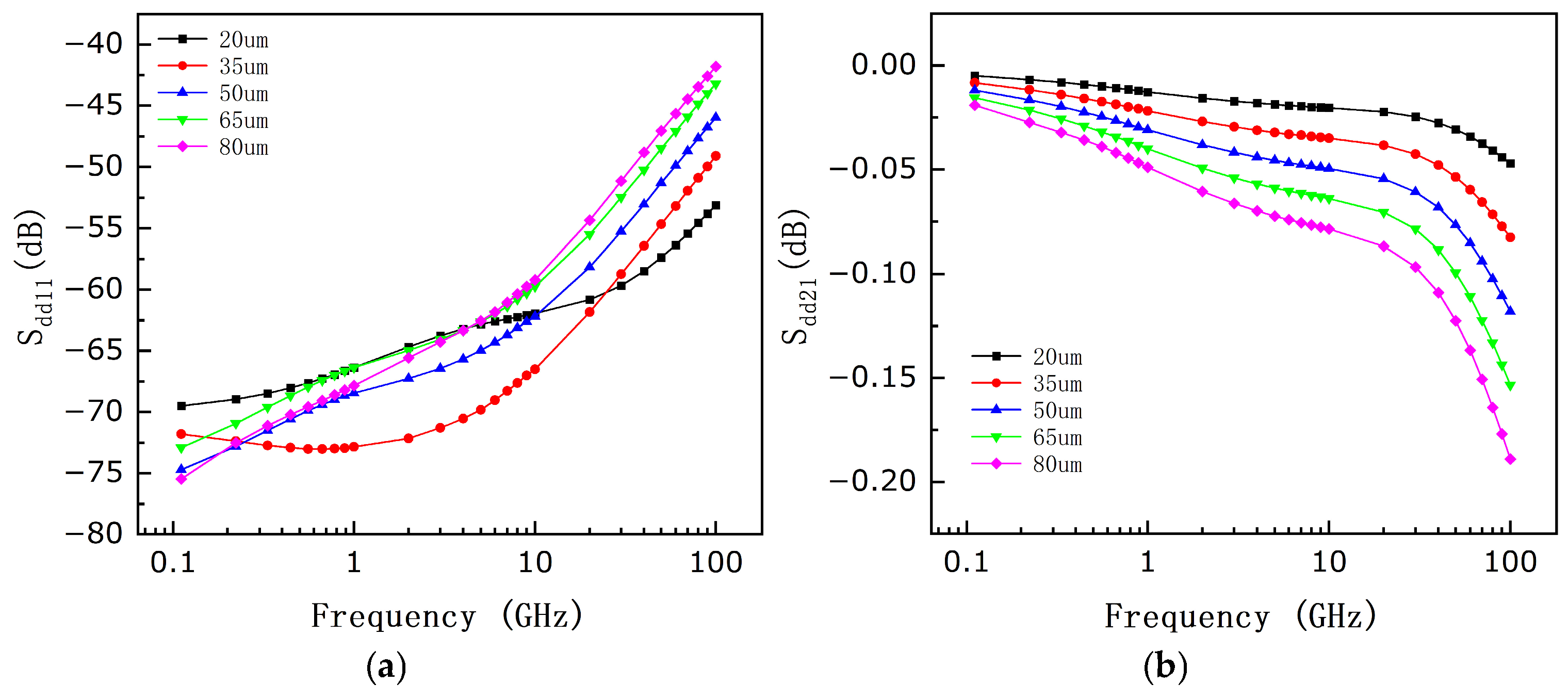
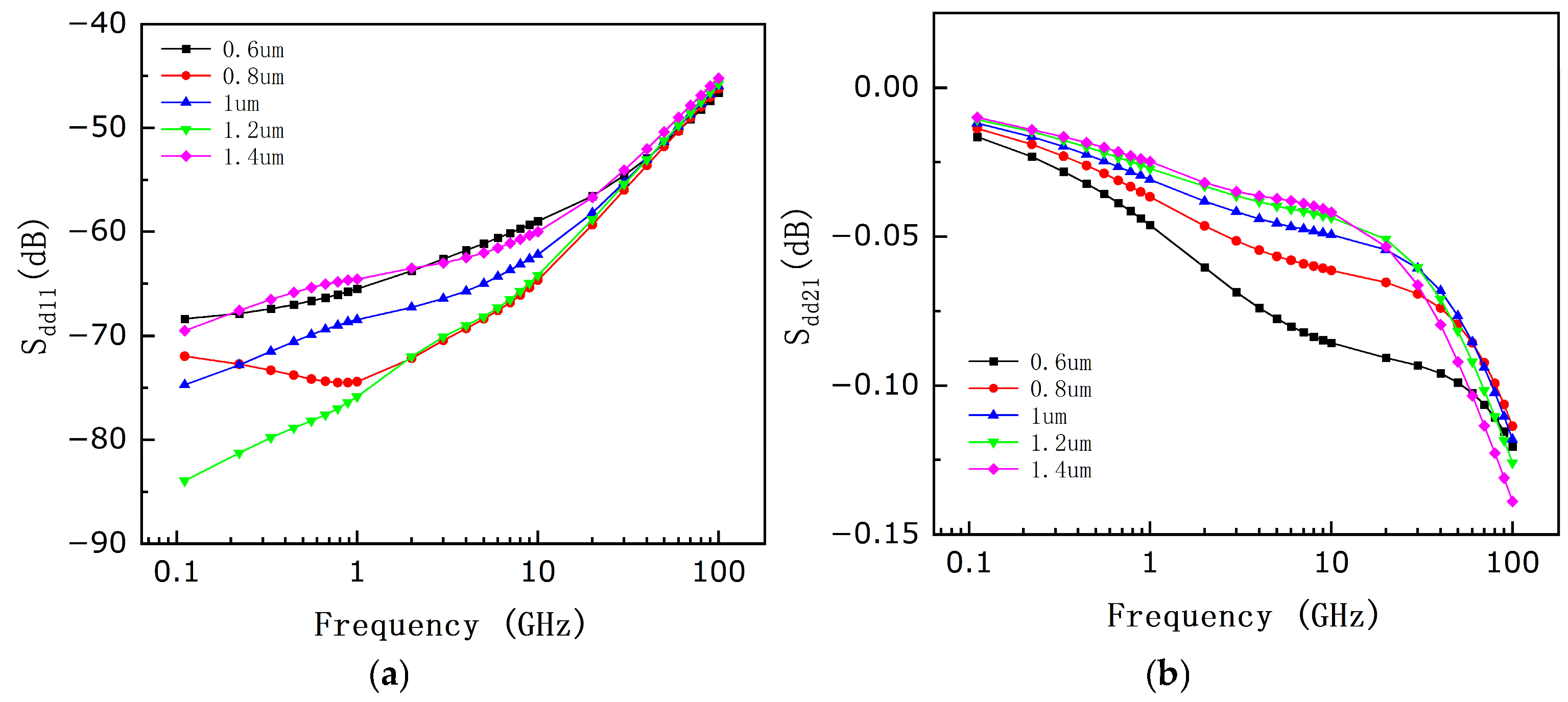
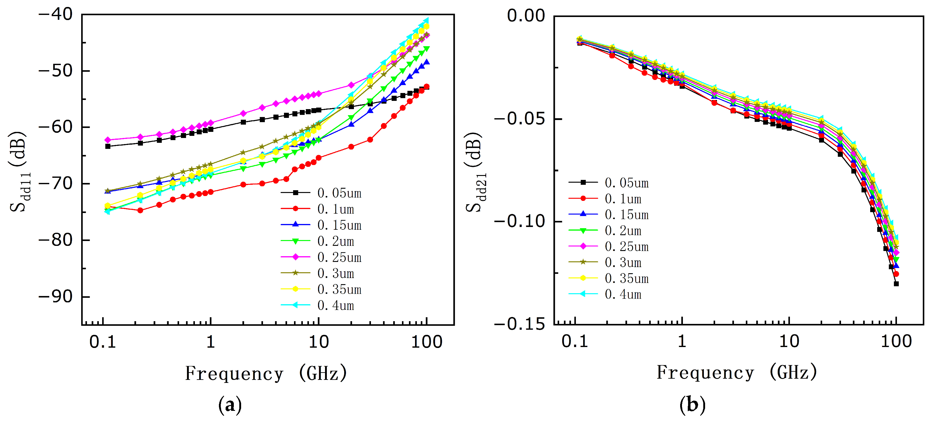
In high-speed circuit design, performance evaluation of differential signal transmission lines primarily relies on S-parameter analysis [18]. Among the S-parameters, Sdd11 and Sdd21 are the two most critical indicators: a higher Sdd11 value indicates more severe impedance discontinuity, which leads to increased signal reflection, resulting in ringing and a higher bit error rate [19,20]. Conversely, Sdd21 represents the energy loss as the signal passes through the transmission line, with a lower value being preferable. Building upon the established accuracy of empirical parasitic parameter extraction, single-variable-based software simulation is employed to analyze the specific influence of each physical structural parameter of shielded quad-axial through-silicon vias (TSVs) on transmission characteristics. Ultimately, optimized TSV structural parameters are derived.
The parasitic parameters of TSVs, such as resistance, inductance, and capacitance, exert a direct influence on the electrical characteristics of 3D IC interconnects, including delay, power consumption, and noise. These parasitic parameters are determined by the geometric configuration and material properties of the TSV. Specifically, the transmission characteristics of the TSV are intrinsically linked to its material attributes and geometric dimensions. Hence, by substituting materials with distinct electrical properties or altering the geometric parameters of the structure, the transmission characteristic of the TSV can be effectively modulated [21,22].
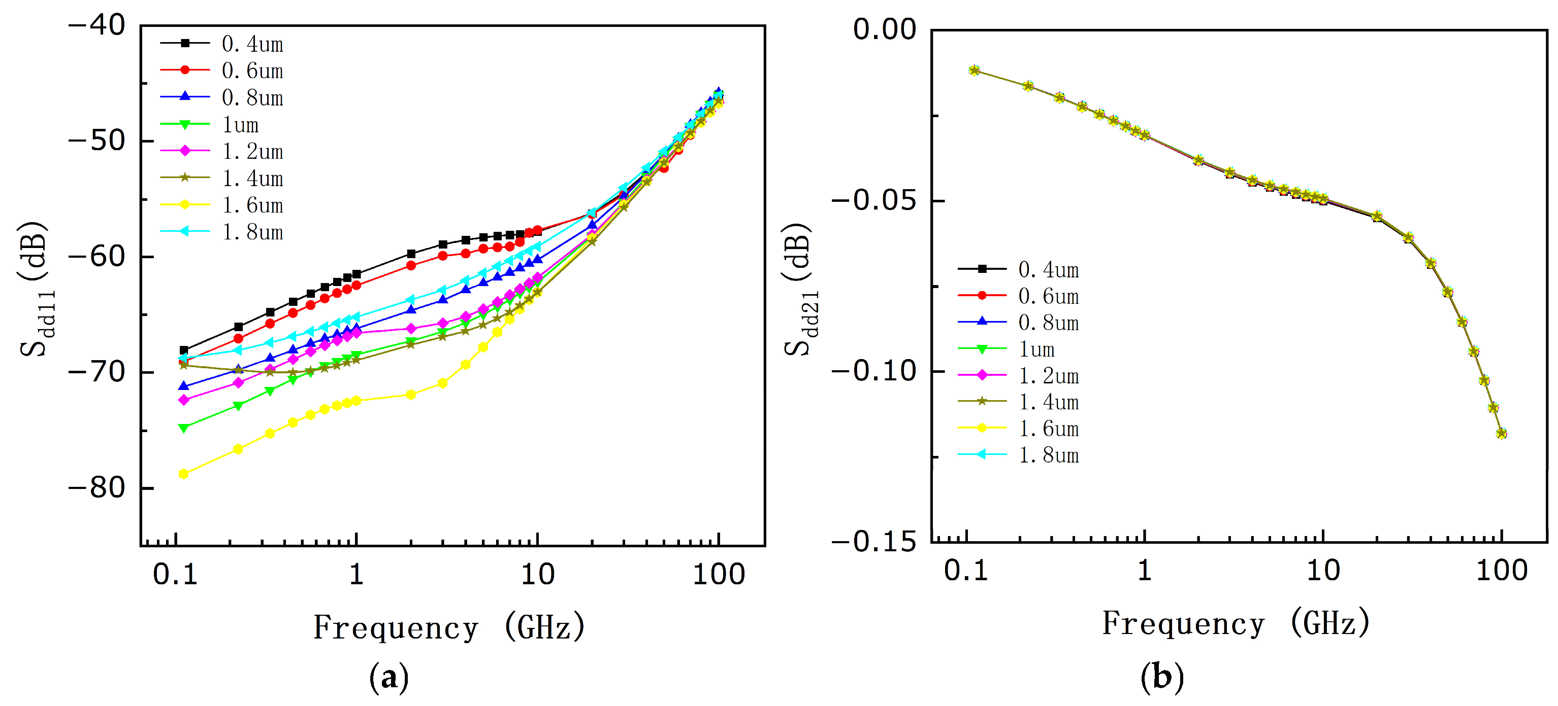
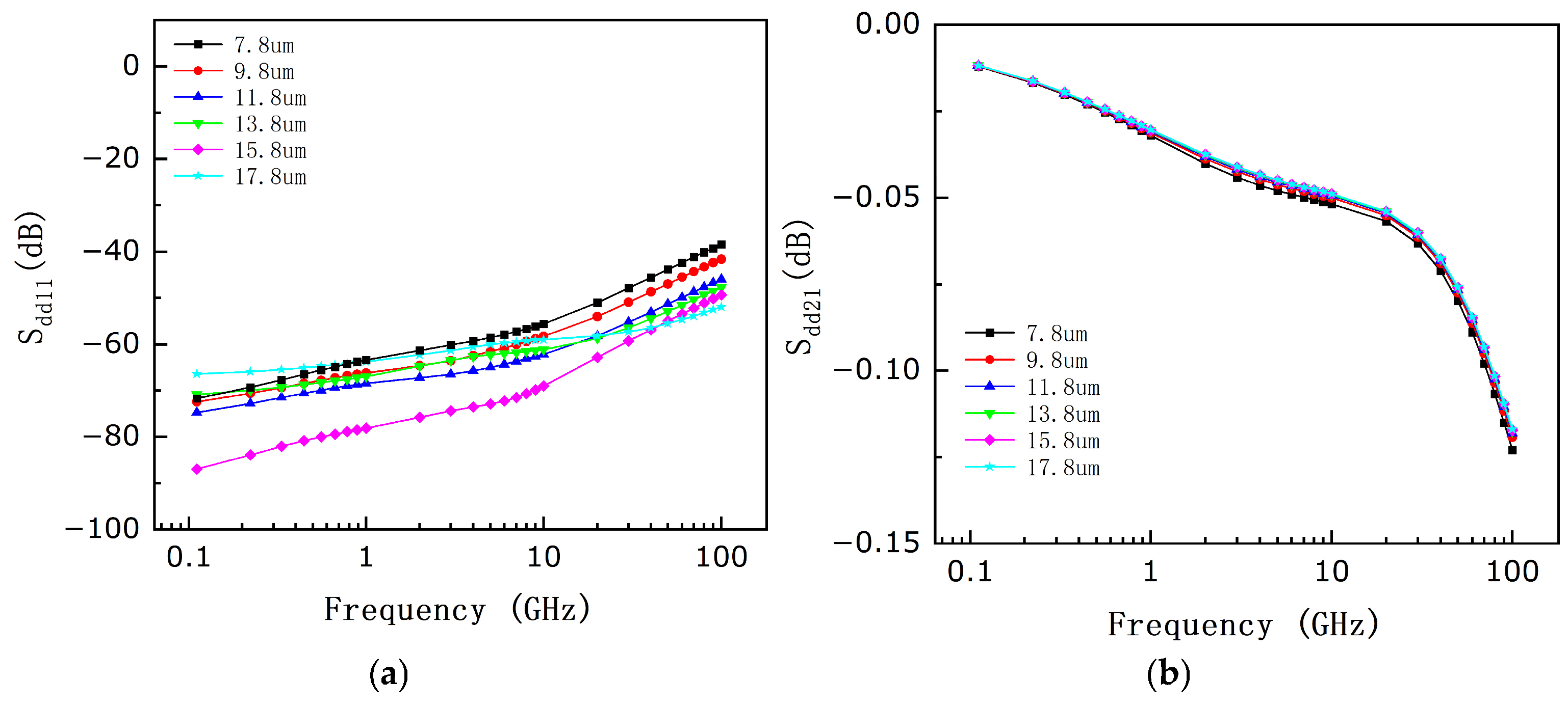
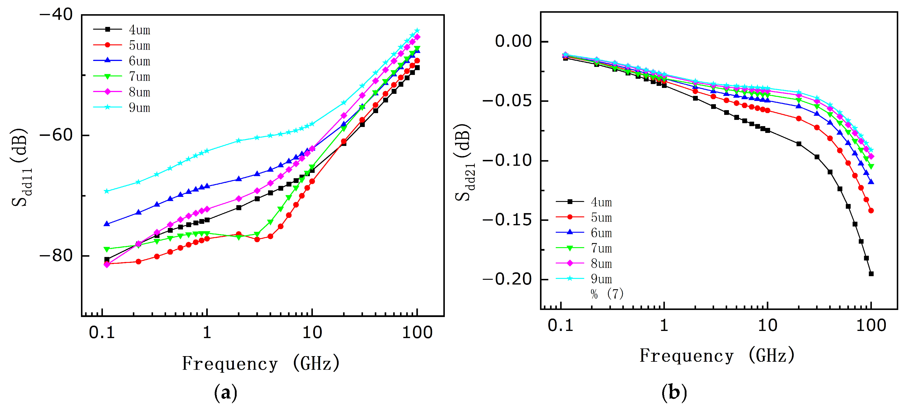
Through systematic investigation into the structural and material parameters of SQDTSVs in Figure 9, Figure 10, Figure 11, Figure 12, Figure 13 and Figure 14, a set of relatively optimal configurations has been derived as illustrated in Table 2. Firstly, the range of values for these parameters was determined through parameter scanning. However, these do not necessarily constitute the absolute optimum. Interdependencies and coupling effects exist among various parameters, where some may impose competing or contradictory influences on parasitic characteristics. Consequently, achieving a universally optimal solution for TSV configurations is unattainable. Instead, within the constraints of existing fabrication technologies, feasible ranges for each parameter are defined, and a suboptimal yet enhanced solution is obtained through combinatorial optimization within these bounds.
The SLNP (Sequential Nonlinear Programming) algorithm is used to obtain the optimal solution for the adjustable parameters. Firstly, the values of the parameters are set as the intermediate values within the optimal range of parameter scanning. Then, the influence magnitudes of height, signal line radius, isolated layer, shielding layer thickness, filled dielectric radius and signal line pitch on Sdd11 and Sdd21 are analyzed. From the results of parameter scanning, it is found that the changes in shielding layer thickness and filled dielectric radius have very little effect on Sdd21. Therefore, the target function for establishing the algorithm can be omitted and the relevant target function for Sdd11 can be directly established. When establishing the target function, equal five-point node selection is adopted for the frequency, and the values of the S parameter corresponding to the frequency are compared with the values from parameter scanning to obtain the maximum value [23]. Finally, the optimal numerical value (SNLP) for the parameters was obtained. Here, the value is rounded to two decimal places.
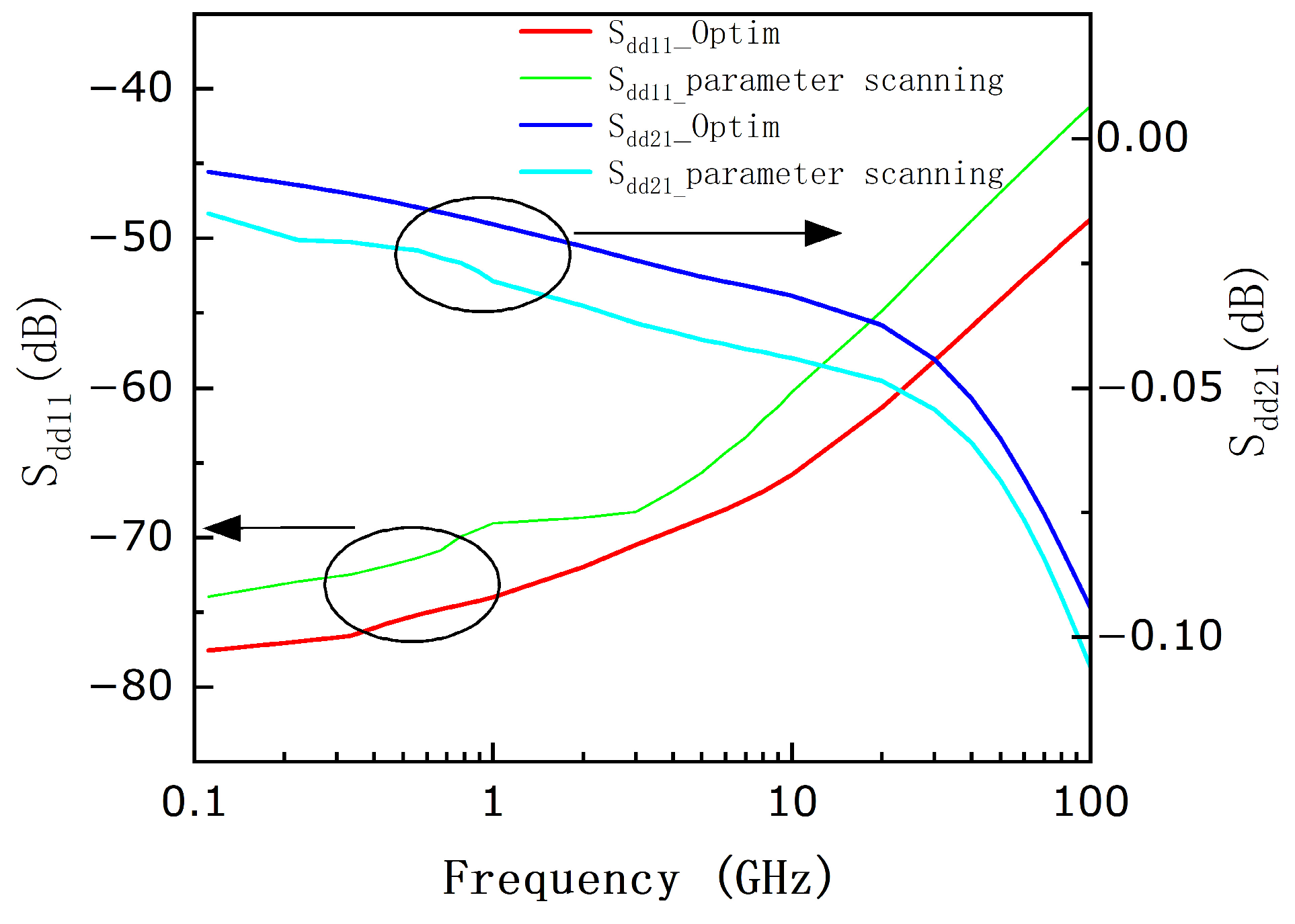
A comparison of the differential-mode S-parameters for the optimized SQDTSV structure with its pre-optimized counterpart in the frequency range of 0–100 GHz is presented in Figure 15, which indicates a marked improvement in transmission performance after optimization.
After comparing the optimized data with the scanned data, it was found that the two sets of data have high stability and excellent matching in the low-frequency range. The differential-mode reflection loss reflects the degree of signal reflection in the transmission line—the lower the value, the smaller the reflection loss. In the low-frequency range of 0 to approximately 0.7 GHz, the Sdd11 value remains at a relatively high level, ranging from approximately −73.16 dB to −70.85 dB, indicating that the TSV structure exhibits excellent input matching characteristics in this frequency range with minimal reflection. The performance in the mid-frequency range significantly deteriorates, starting from 1 GHz, with the S11 value showing a clear downward trend, dropping rapidly from −69.05615 dB to −60.25026 dB at 10 GHz. Within this range, for every doubling of frequency, S11 deteriorates by approximately 5–8 dB, indicating that as the frequency increases, the structural mismatch intensifies and the reflection energy significantly increases [24]. In the high-frequency range from 20 GHz to 100 GHz [25], Sdd11 further deteriorates, dropping from −54.84149 dB to −41.13493 dB, with a cumulative deterioration of over 13 dB. Although the absolute values are still decreasing, the deterioration rate shows a marginal decreasing trend. The optimized model of the structure has a full-frequency performance advantage in the interpolation reflection loss. This means that the suppression ability of reflected power is significantly enhanced. Especially in the 50–100 GHz high-frequency range, the improvement is more significant, and at this time, the difference between the two sets of data shows an expanding trend, with the difference being above 6.98 dB.
Common-mode insertion loss reflects the efficiency of signal transmission along the line. The higher the value, the better the effect of the signal transmission to the receiving end. The overall trend of the common-mode insertion loss of the two sets of data is monotonic attenuation with an increase in frequency. Optimized data comparison parameter scanning shows better common-mode insertion loss characteristics throughout the frequency range. Its value is closer to zero, indicating that the optimized TSV structure has lower energy loss and higher transmission efficiency during signal transmission. In the low-frequency range of 0–10 GHz, the loss reduction of the optimized design is higher than 27%, and in the low-frequency range of 10–100 GHz, the loss reduction of the optimized design is higher than 11%. Although the absolute gain slightly narrows, considering that the parasitic effect has reached saturation at high frequencies, it can still achieve a loss improvement of more than 10%, which has important engineering value.

4. Conclusions

This paper presents a shielded quad-axial differential through-silicon via (TSV) structure and extracts its parasitic parameters using MATLAB for computational analysis. To verify the accuracy of these parameters, the simulation values of resistance (R) and inductance (L) were obtained using the HFSS simulation tool, thereby validating the correctness of the analytical formulae for each parameter. Employing the single-variable method, multiple key parameters of the proposed shielded quad-axial differential TSV model—including height, signal line radius, isolated layer, shielding layer thickness, filled dielectric radius, signal line pitch, and relative permittivity of the filled dielectric—were systematically investigated. Only one parameter was altered at a time while keeping the others at their default initial values, enabling the determination of near-optimal values for each parameter. Subsequently, these optimized parameters were integrated. Throughout the optimization process, adjustments to each parameter led to complex variations in performance, particularly regarding the relative weight of parasitic parameters and their impact on transmission characteristics, which changed dynamically with parameter modifications. Ultimately, the optimized structure achieved significant enhancement in transmission performance.

Author Contributions

Conceptualization, methodology and project administration, J.L. and Z.P.; software, validation, formal analysis, writing—original draft preparation, writing—review and editing, J.L.; supervision, Z.P. All authors have read and agreed to the published version of the manuscript.

Funding

This research received no external funding.

Data Availability Statement

Data sharing is not applicable.

Conflicts of Interest

The authors declare no conflict of interest.

References

  1. William, S. Semiconductive Wafer and Method of Making the Same. U.S. Patent 3,044,909, 17 July 1962. [Google Scholar]
  2. Kilby, J.S. Invention of the integrated circuit. IEEE Trans. Electron Devices 1976, 23, 648–654. [Google Scholar] [CrossRef]
  3. Guan, Y.; Ma, S.; Zeng, Q.; Chen, J.; Jin, Y. Fabrication and characterization of annular copper throughsilicon via for passive interposer applications. IEEE Trans. Semicond. Manuf. 2018, 31, 270–276. [Google Scholar] [CrossRef]
  4. Li, J.M.; Liang, H.G.; Lv, H.; Pan, Y.Q.; Huang, Z.; Chen, T.; Lu, Y. Machine Learning-Based Diagnosis of Defects in 2.5-D and 3-D Interconnects. IEEE Trans. Compon. Packag. Manuf. Technol. 2025, 15, 1104–1116. [Google Scholar] [CrossRef]
  5. Wenle, Z.; Mong, K.Y.; Guan, L.T.; Damaruganath, P.; Hwa, T.K.; Xiaowu, Z. Study of high speed interconnects of multiple dies stack structure with Through-Silicon-Via (TSV). In IEEE Electrical Design of Advanced Package & Systems Symposium; IEEE: Singapore, 2010; pp. 1–4. [Google Scholar]
  6. Zhao, W.S.; Yin, W.Y.; Wang, X.P.; Xu, X.L. Frequency- and temperature-dependent modeling of coaxial through-silicon vias for 3-D ICs. IEEE Trans. Electron Devices 2011, 58, 3358–3368. [Google Scholar] [CrossRef]
  7. Liang, F.; Wang, G.; Zhao, D.; Wang, B.Z. Wideband impedance model for coaxial through-silicon vias in 3-D integration. IEEE Trans. Electron Devices 2013, 60, 2498–2504. [Google Scholar] [CrossRef]
  8. Lu, Q.; Zhu, Z.; Yang, Y.; Ding, R. Electrical Modeling and Characterization of Shield Differential Through-Silicon Vias. IEEE Trans. Electron Devices 2015, 62, 1544–1552. [Google Scholar] [CrossRef]
  9. Xu, Z.; Lu, J.Q. Three-dimensional coaxial through-silicon via (TSV) design. IEEE Electron Device Lett. 2012, 33, 1441–1443. [Google Scholar] [CrossRef]
  10. Zhao, W.S.; Zheng, J.; Liang, F.; Xu, K.; Chen, X.; Wang, G. Wideband Modeling and Characterization of Differential Through-Silicon Vias for 3-D ICs. IEEE Trans. Electron Devices 2016, 63, 1168–1175. [Google Scholar] [CrossRef]
  11. Ndip, I.; Curran, B.; Lobbicke, K.; Guttowski, S.; Reichl, H.; Lang, K.D.; Henke, H. High-frequency modeling of TSVs for 3-D chip integration and silicon interposers considering skin-effect, dielectric quasi-TEM and slow-wave modes. IEEE Trans. Compon. Packag. Manuf. Technol. 2011, 1, 1627–1641. [Google Scholar] [CrossRef]
  12. Schelkunoff, S.A. The electromagnetic theory of coaxial transmission lines and cylindricalshields. Bell Syst. Tech. J. 1934, 13, 532–579. [Google Scholar] [CrossRef]
  13. Paul, C.R. Inductance: Loop and Partial; Wiley: New York, NY, USA, 2010. [Google Scholar]
  14. Paul, C.R. Analysis of Multiconductor Transmission Lines, 2nd ed.; Wiley: New York, NY, USA, 2008. [Google Scholar]
  15. Bandyopadhyay, T.; Han, K.J.; Chung, D.; Chatterjee, R.; Swaminathan, M.; Tummala, R. Rigorous electrical modeling of through silicon vias (TSVs) with MOS capacitance effects. IEEE Trans. Compon. Packag. Manuf. Technol. 2011, 1, 893–903. [Google Scholar] [CrossRef]
  16. Kim, J.; Cho, J.; Kim, J.; Yook, J.M.; Kim, J.C.; Lee, J.; Park, K.; Pak, J.S. High-frequency scalable modeling and analysis of a differential signal through-silicon via. IEEE Trans. Compon. Packag. Manuf. Technol. 2014, 4, 697–707. [Google Scholar] [CrossRef]
  17. Lu, K.C.; Horng, T.S. Wideband and scalable equivalent-circuit model for differential through silicon vias with measurement verification. In Proceedings of the 2013 IEEE 63rd Electronic Components and Technology Conference, Las Vegas, NV, USA, 28–31 May 2013; pp. 1186–1189. [Google Scholar]
  18. Li, J.W.; Pan, Z.L. Electrical modeling and characterization of shield double differential through-silicon vias (SDDTSVs). In Proceedings of the International Conference on Signal Processing, Communication, and Control Systems (SPCCS 2025), Hangzhou, China, 28–30 March 2025; Volume 13705, pp. 1–6. [Google Scholar]
  19. Izadi, Y.; Beiranvand, R. A Comprehensive Review of Battery and Supercapacitor Cells Voltage-Equalizer Circuits. IEEE Trans. Power Electron. 2023, 38, 15671–15692. [Google Scholar] [CrossRef]
  20. Kim, H.; Park, J.; Lee, S.; Kim, J.; Ahn, S. Signal Integrity Analysis of Through-Silicon-Via (TSV) with Passive Equalizer to Separate Return Path and Mitigate the Inter-Symbol Interference (ISI) for Next Generation High Bandwidth Memory. IEEE Trans. Compon. Packag. Manuf. Technol. 2023, 13, 1973–1988. [Google Scholar] [CrossRef]
  21. Abdullah, M.F.; Lee, H.W. Technology review of CNTs TSV in 3D IC and 2.5D packaging: Progress and challenges from an electrical viewpoint. Microelectron. Eng. 2024, 290, 23–27. [Google Scholar] [CrossRef]
  22. Moreau, S.; Thomas, C.; Bouchu, D. Assessing Copper High Density-TSVs for Reliable Performance in Cryogenic Systems. IEEE Electron Device Lett. 2025, 46, 80–83. [Google Scholar] [CrossRef]
  23. Ju, J.Y.; Liu, Q.Q.; Zhang, P.; Wang, J.; Zhao, P.; Lin, X.; Yao, C.Y.; Zhao, W.S. Distribution Optimization of Through-Silicon Via (TSV) Array Based on Genetic Algorithm. IEEE Trans. Compon. Packag. Manuf. Technol. 2025, 15, 399–409. [Google Scholar] [CrossRef]
  24. Wang, L.H.; Dong, G.; Zhi, C.L.; Zhu, Z.M. Prebond TSV Detection for Coexistence of Open and Leakage Faults Based on Current Charging and Discharging. IEEE Trans. Compon. Packag. Manuf. Technol. 2025, 15, 1091–1103. [Google Scholar] [CrossRef]
  25. Yi, H.Y.; Zhu, J.Y.; Fan, J.W.; Wang, D.G.; Mao, J.F. Through-silicon via advanced packaging technology and its radio frequency applications. Chip 2026, 5, 100158. [Google Scholar] [CrossRef]
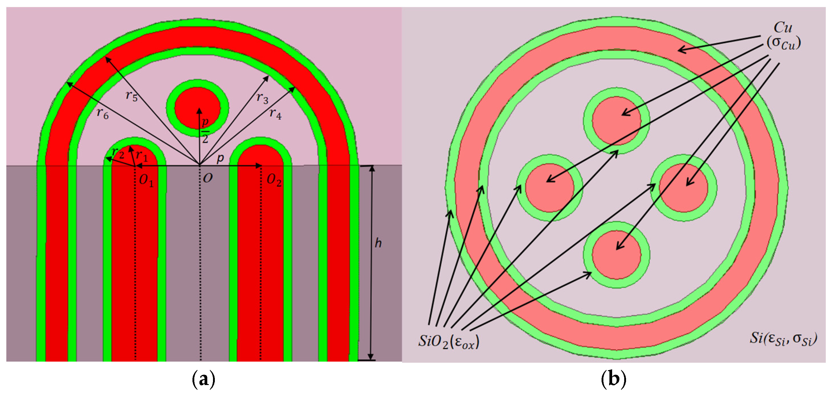
Figure 1. (a) 3D view and (b) cross-sectional view of SQDTSV configuration.
Electronics 15 02186 g001
Figure 2. Comparison of the results of resistances obtained from the HFSS simulation and the analytical calculation.
Electronics 15 02186 g002
Figure 3. Comparison of the results of inductance and mutual inductance obtained from the HFSS simulation and the analytical calculation.
Electronics 15 02186 g003
Figure 4. Comparison of the results of capacitance and mutual capacitance obtained from the HFSS simulation and the analytical calculation.
Electronics 15 02186 g004
Figure 5. Comparison of the results of conductance and mutual conductance obtained from the HFSS simulation and the analytical calculation.
Electronics 15 02186 g005
Figure 6. Equivalent circuit model of SQDTSVs.
Electronics 15 02186 g006
Figure 7. Comparison of the SQDTSVs of S d d 11 and the SDTSVs of S d d 11 obtained from the HFSS simulation.
Electronics 15 02186 g007
Figure 8. Comparison of the SQDTSVs of S d d 21 and the SDTSVs of S d d 21 obtained from the HFSS simulation.
Electronics 15 02186 g008
Figure 9. The S-parameters of SQDTSVs at different heights (h): (a) S d d 11 ; (b) S d d 21 .
Electronics 15 02186 g009
Figure 10. The S-parameters of SQDTSVs at different signal line radii ( r 1 ): (a) S d d 11 ; (b) S d d 21 .
Electronics 15 02186 g010
Figure 11. The S-parameters of SQDTSVs at different isolated layers ( t o x ): (a) S d d 11 ; (b) S d d 21 .
Electronics 15 02186 g011
Figure 12. The S-parameters of SQDTSVs at different shielding layer thicknesses ( t 1 ): (a) S d d 11 ; (b) S d d 21 .
Electronics 15 02186 g012
Figure 13. The S-parameters of SQDTSVs at different filled dielectric radii ( r 3 ): (a) S d d 11 ; (b) S d d 21 .
Electronics 15 02186 g013
Figure 14. The S-parameters of SQDTSVs at different signal line pitches ( ρ ): (a) S d d 1 ; (b) S d d 21 .
Electronics 15 02186 g014
Figure 15. Comparative analysis of S-parameters between conventional and optimized SQDTSV structures.
Electronics 15 02186 g015
Table 1. Quantitative comparison of TSVs of coaxial, GSSG, and SDTSV types.
Comparison TypeSDTSVsCoaxial TSVsGSSG TSVs
Frequency rangeUp to 100 GHz [8].1–40 GHz [9].High-frequency applications [10].
Complexity of processSimilar to coaxial TSVs but without the need for additional steps.A coaxial structure needs to be formed.The GSSG structure needs to be precisely arranged and occupies a large amount of space.
Electromagnetic shielding effectSimilar to coaxial TSV.The copper ring effectively shields the electromagnetic field.The effect is relatively poor.
AdvantageThe S parameters exhibit excellent matching over a frequency range of up to 100 GHz.
The peripheral metal layer not only serves as a shielding layer to suppress surrounding electromagnetic interference, but also acts as a return path for the internal differential transmission lines, thereby improving the utilization of resources.
Reduce signal attenuation by 35% and time delay by 25%.
No additional grounding for TSV.
Effectively suppress noise coupling and electromagnetic interference.
Modeling and measurement have been successfully accomplished at high frequencies.
Table 2. Structural parameter scanning of SQDTSV and optimized SQDTSV parameters.
Symbolic RepresentationThe Range of Optimization Obtained Through Parameter ScanningThe Optimized Numerical Value (SNLP)
Heighth20–35 μm31.69 μm
Signal line radius r 1 1–1.2 μm1.18 μm
Isolated layer t o x 0.1–0.15 μm0.12 μm
Shielding layer thickness t 1 = r 5 r 4 1.4–1.6 μm1.47 μm
Filled dielectric radius r 3 13.8–15.8 μm14.37 μm
Signal line pitchp5–6 μm5.32 μm
Disclaimer/Publisher’s Note: The statements, opinions and data contained in all publications are solely those of the individual author(s) and contributor(s) and not of MDPI and/or the editor(s). MDPI and/or the editor(s) disclaim responsibility for any injury to people or property resulting from any ideas, methods, instructions or products referred to in the content.