1. Introduction
The rapid advancement of artificial intelligence (AI) and machine learning applications has created an unprecedented demand for high-performance, low-power memory subsystems. Traditional von Neumann architectures face limitations due to the memory bottleneck, where frequent data transfers between the processor and memory result in excessive latency and energy consumption. Computing-in-memory (CIM) has emerged as a promising paradigm to mitigate this challenge by enabling computation within the memory array itself [
1].
Static Random-Access Memory (SRAM) is a critical component of CIM architectures due to its high-speed operation and compatibility with logic integration. While conventional binary SRAM architectures using CMOS and FinFET technologies have demonstrated scalability, their binary nature limits storage efficiency and computational density. A recent study proposed an 8T SRAM structure based on binary CMOS and FinFET design [
2], demonstrating improvements in stability and energy efficiency. However, binary SRAM inherently restricts data representation to two states.
Ternary SRAM architectures, which operate with three logic states (e.g., −1, 0, and +1), can enhance data storage density and reduce interconnect complexity, making them highly attractive for AI accelerators. In parallel, emerging transistor technologies such as Carbon Nanotube Field-Effect Transistors (CNFETs) and Gate-All-Around Field-Effect Transistors (GAAFETs) have shown promise in overcoming the scaling limitations of CMOS and FinFET devices. This paper investigates the low-power performance of a sense-amplifier embedded (SE) ternary 9T SRAM CIM architecture designed using CNFET and GAAFET technologies, comparing their effectiveness in AI hardware applications.
2. Background
Large-scale parallel data processing is often required in AI-driven applications, leading to significant energy consumption. SRAM-based compute-in-memory (CIM) architectures address this challenge by performing computations directly within memory arrays, thereby minimizing data movement and reducing power dissipation. The use of ternary logic further enhances energy efficiency by decreasing the number of required logic operations, resulting in lower power consumption compared to traditional binary designs [
3]. Within ternary logic systems, the XNOR gate plays a vital role, particularly in arithmetic and comparison functions. The integration of ternary XNOR operations into 8T SRAM cells enables efficient in-memory computation, improving processing speed while reducing power consumption and latency. Consequently, these architectures are well suited for AI applications that demand high-speed operation with minimal energy usage.
2.1. Ternary SRAM and CIM Architectures
Conventional SRAM cells store binary data, requiring more transistors and interconnects as memory size scales. Ternary SRAM, by contrast, can store three logic levels per cell, reducing the number of cells required to store the same information. This enables improved density and power efficiency in CIM applications. The sense-amplifier embedded (SE) design further improves read stability and energy efficiency, making it suitable for low-power AI workloads.
2.2. Pass Transistor Logic
Digital circuits can be realized using pass transistor logic (PTL), a design approach in which transistors directly propagate input signals instead of generating outputs through conventional voltage-level switching. In standard CMOS logic, output nodes are driven to logic high or low by complementary PMOS and NMOS transistor networks based on the input states. In contrast, PTL employs transistors as controlled switches that selectively permit or inhibit the transmission of voltage signals. This approach can lead to reduced transistor count, lower power dissipation, and faster switching performance.
In PTL, PMOS transistors are effective at passing a strong logic “1” but exhibit degraded performance when transmitting a logic “0”, whereas NMOS transistors efficiently pass a logic “0” but suffer from threshold voltage loss when passing a logic “1”. As a result, both NMOS and PMOS devices are often used together to achieve full-swing signal transmission, enabling reliable logic operation [
4,
5].
2.3. CNFET
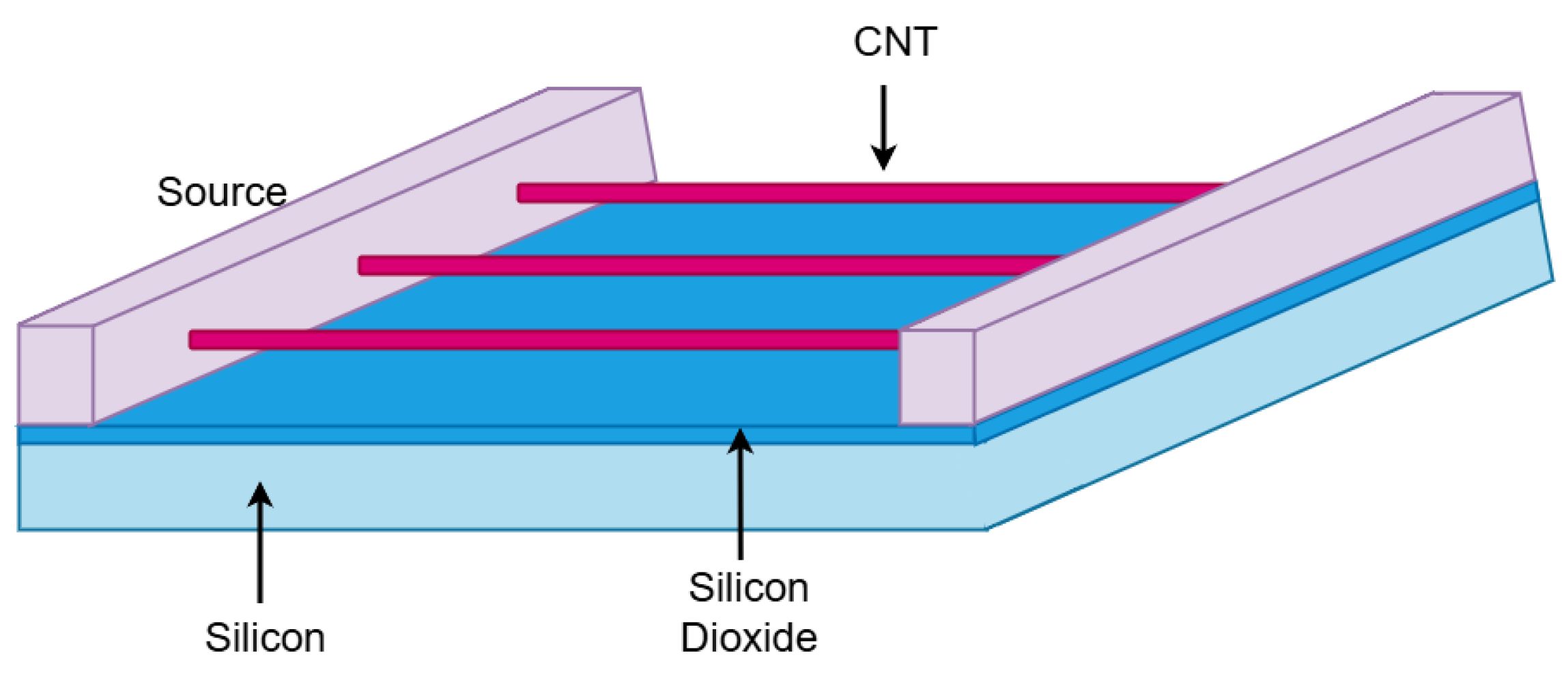
A Carbon Nanotube Field-Effect Transistor (CNFET) (
Figure 1) is an emerging device technology in which the conventional silicon channel is replaced by carbon nanotubes (CNTs). These CNTs are cylindrical graphene-based nanostructures that exhibit outstanding electrical properties—including near-ballistic carrier transport, high mobility, and a very low subthreshold swing—making CNFETs strong candidates for extending device scaling beyond the limits of CMOS technologies [
6]. For all simulations in this work, the CNFET model uses a CNT diameter of 1.4 nm, a chirality of (19,0), a mean free path of 200 nm, a contact resistance of 6.5 kΩ, and two CNTs per device.
In a CNFET, one or more semiconducting nanotubes form the conduction channel between the source and drain terminals, while the gate controls carrier transport. Owing to the quasi-ballistic nature of CNT channels, carriers experience minimal scattering, enabling faster switching and lower energy dissipation. Additionally, the one-dimensional geometry of CNTs provides excellent gate electrostatic control, allowing transitions between ON and OFF states with small variations in gate voltage and thereby reducing power consumption.
Despite these advantages, the practical realization of CNFET technology involves several fabrication challenges, including the precise placement of CNTs, removal of metallic nanotubes, and maintaining uniform alignment across large wafers. Nonetheless, recent progress has demonstrated functional logic circuits, memory cells, and even prototype microprocessors based on CNFET technology [
7]. Owing to their superior electrical characteristics, low-power operation, and scalability, CNFETs remain highly promising for future generations of memory, processor, and compute-in-memory architectures.
2.4. GAAFET
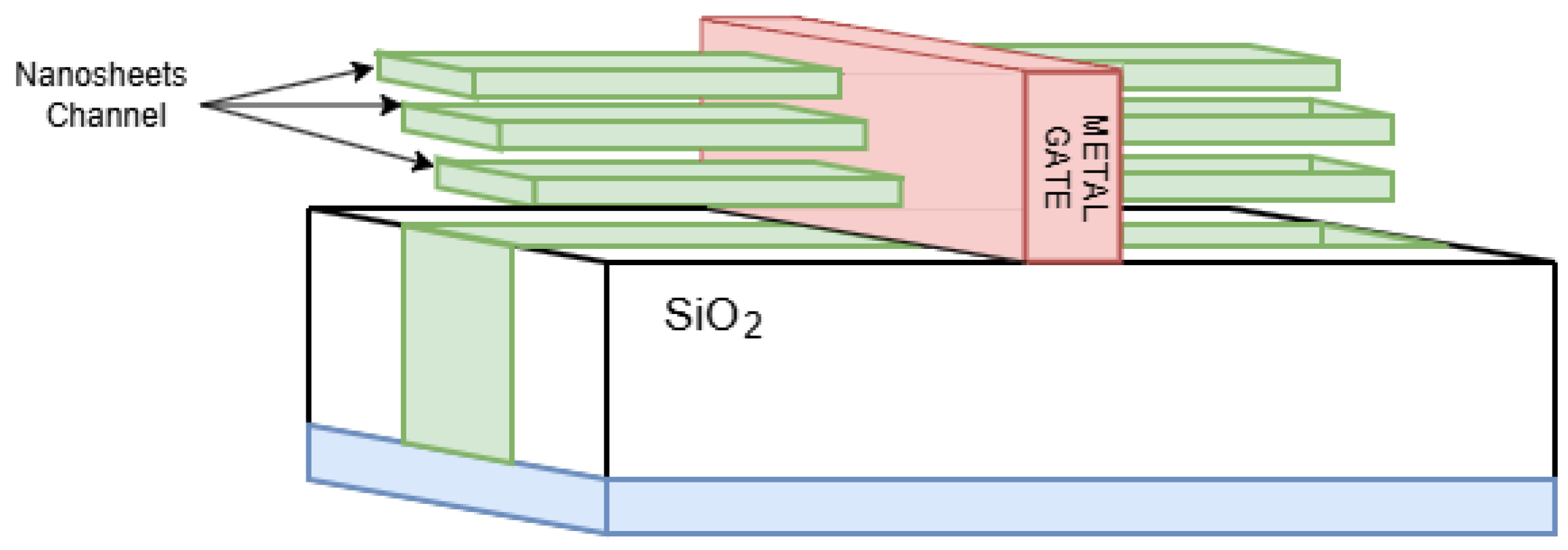
The Gate-All-Around Field-Effect Transistor (GAAFET) is an advanced device architecture designed to overcome the scaling limitations of FinFETs as technology nodes shrink below 5 nm. In planar MOSFETs and FinFETs, the gate controls the channel from one side or three sides, respectively. As dimensions continue to scale, these structures face challenges such as increased short-channel effects, higher leakage, and reduced electrostatic control. GAAFET addresses these issues by completely surrounding the channel with the gate—hence the term “gate-all-around”—as illustrated in
Figure 2. This fully wrapped gate configuration significantly improves electrostatics, resulting in reduced off-state leakage, lower drain-induced barrier lowering (DIBL), and an improved subthreshold slope. The GAAFET model used in this work employs nanosheets with a width of 12 nm, a thickness of 5 nm, an oxide thickness of 1.2 nm, and a threshold voltage of 0.32 V.
Structurally, GAAFETs typically use stacked horizontal nanosheets or nanowires rather than the vertical fins used in FinFETs. These nanosheets are entirely enclosed by the gate, offering superior control over channel conduction. A key advantage of this architecture is the ability to tune the drive current by modifying the number or dimensions of the nanosheets, providing greater design flexibility for optimizing power and performance. The increased gate–channel interface area further enhances electrostatic control, enabling continued device scaling without compromising reliability or drive strength.
Owing to their excellent balance of high performance and low power consumption, GAAFETs are well-suited for applications such as processors, system-on-chip (SoC) platforms, SRAM, and compute-in-memory (CIM) architectures. Major semiconductor manufacturers have already begun transitioning to GAAFET-based technologies—for example, Intel’s RibbonFET architecture and TSMC and Samsung’s forthcoming GAAFET nodes. Overall, GAAFET represents a significant advancement in transistor design, supporting Moore’s Law by combining high drive current, reduced leakage, and superior scalability within a compact device structure [
8].
2.5. Comparison Between GAAFET and CNFET
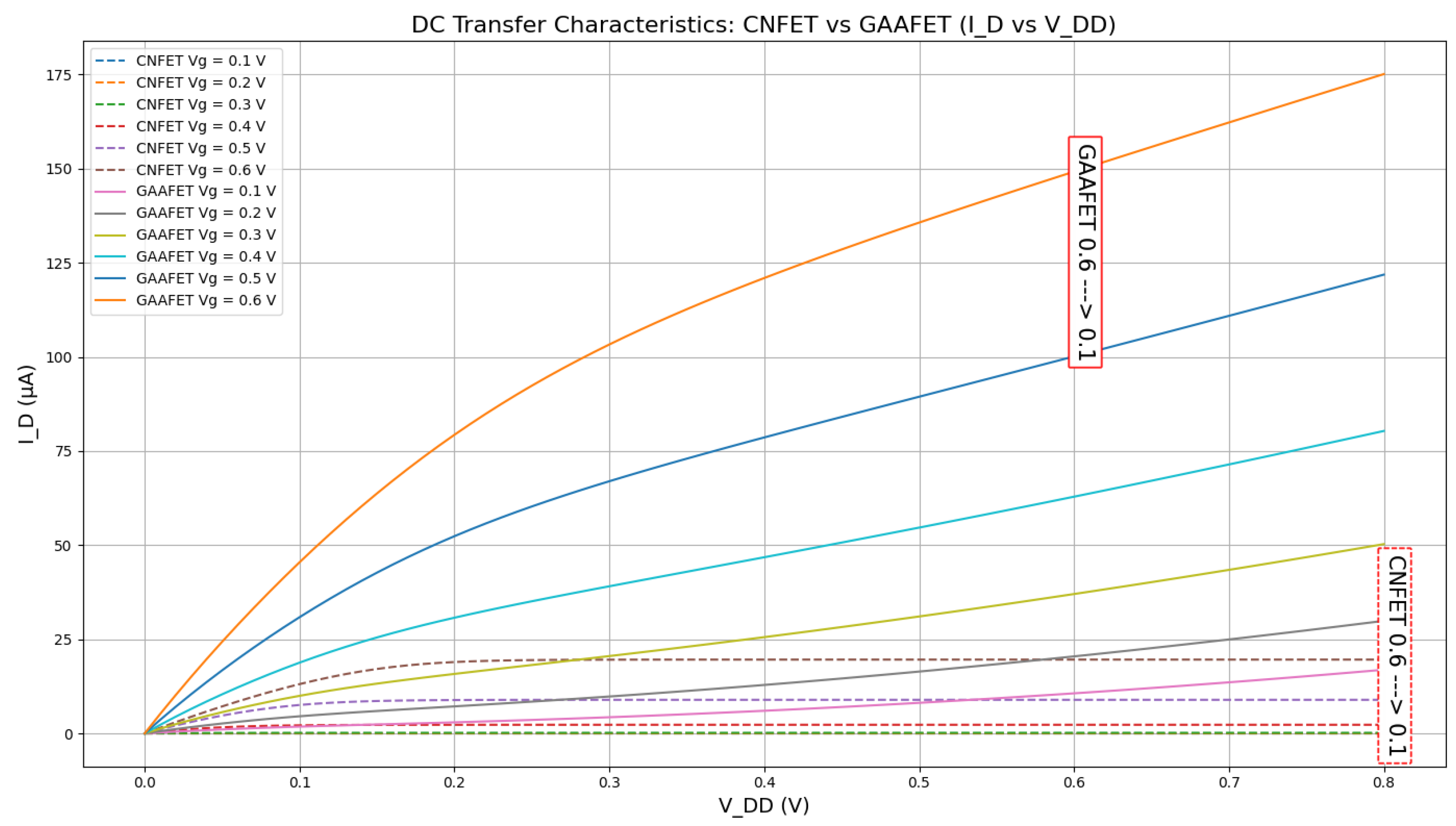
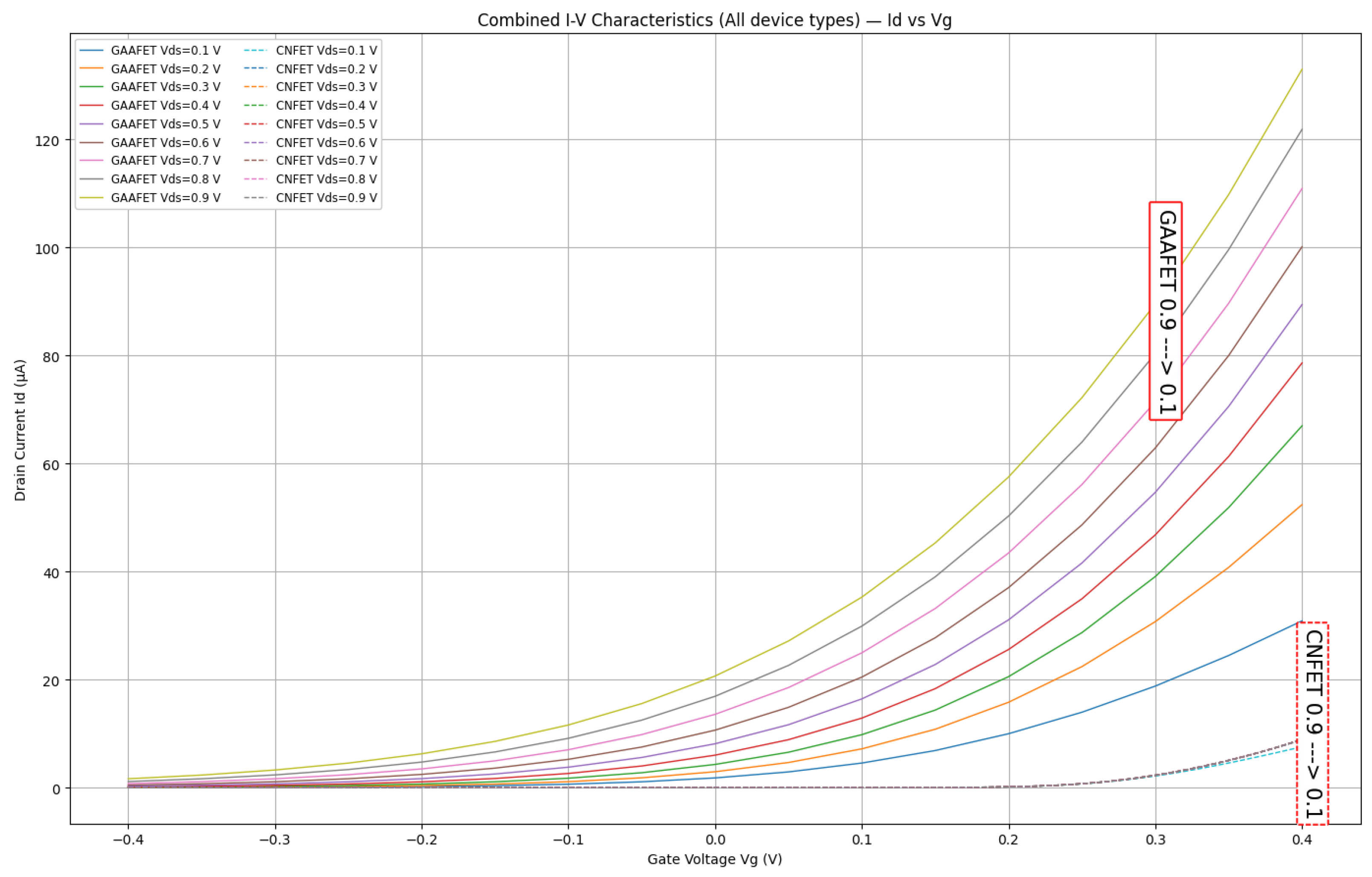
The I–V characteristics of GAAFET and CNFET devices, as shown in
Figure 3 and
Figure 4, demonstrate distinct behaviors owing to their fundamental structural and material differences.
Figure 4 illustrates the drain current (I_D) versus drain-to-source voltage (V_DS) characteristics for various gate voltages (V_G). It is evident that GAAFET exhibits significantly higher drive current across all V_G values, with a peak I_D of approximately 175 µA at V_G = 0.6 V and V_DS = 0.8 V. The I_D increases steadily with V_DS, showing a clear transition from the linear to saturation region. In contrast, CNFET exhibits early saturation behavior, with I_D quickly plateauing beyond V_DS = 0.2 V for all V_G. The maximum current observed for CNFET is 27 µA at the highest bias, indicating strong saturation and low drain-induced barrier lowering (DIBL) due to its quasi-ballistic transport.
Figure 4 presents I_D versus gate voltage (V_G) for various V_DS values. GAAFET shows strong current modulation with V_G, with I_D increasing sharply in the strong inversion region. At V_DS = 0.9 V, the maximum I_D exceeds 130 µA. The GAAFET curves also demonstrate good gate control and scalability, typical of advanced silicon devices with excellent short-channel suppression. On the other hand, CNFET shows a much steeper subthreshold slope and lower leakage current, with I_D remaining below 10 µA for all V_DS values. The abrupt increase in I_D at low V_G in CNFET is attributed to the near-ideal electrostatics and 1D conduction of carbon nanotubes, which minimize short-channel effects and enable efficient low-power switching [
9].
In summary, the comparative I–V graphs highlight that GAAFET provides higher drive strength, making it suitable for high-performance applications [
10]. At the same time, CNFET offers superior subthreshold behavior and energy efficiency, making it ideal for low-power, high-speed circuits. The early current saturation and low off-state leakage in CNFETs also underscore its potential to scale beyond silicon limits in future nanoelectronic systems [
11].
2.6. Fabrication Issues in CNFET and GAAFET-Based SRAMs
Despite their potential, both CNFET and GAAFET technologies face practical fabrication hurdles:
CNFET
- −
Difficulty in achieving uniform chirality and semiconducting CNT growth;
- −
Metallic CNT removal requires high-precision post-growth techniques;
- −
Alignment and placement of CNTs at wafer scale remain unsolved challenges;
- −
Reliability issues due to CNT junction defects.
GAAFET
- −
Complex fabrication steps compared to FinFET (stacked nanosheets/nanowires require precise etching);
- −
Variability in nanosheet dimensions leads to threshold voltage variations;
- −
Increased parasitic capacitance from multi-stack configurations;
- −
Higher manufacturing costs due to new process steps and equipment.
Understanding these fabrication limitations is essential in evaluating the practicality of deploying CNFET- and GAAFET-based ternary SRAM in large-scale AI hardware systems [
12,
13].
3. Design of Ternary XNOR Circuits Using Pass Transistor Logic
In binary logic, an XNOR gate outputs a ‘1’ when the two inputs are equal and a ‘0’ when they differ. In ternary logic systems, however, the signals take three values:
, 0, and
. When extended to ternary arithmetic, the XNOR operation produces a
neutral output (0) when the input conditions balance, and outputs
or
depending on the similarity between the operands [
14].
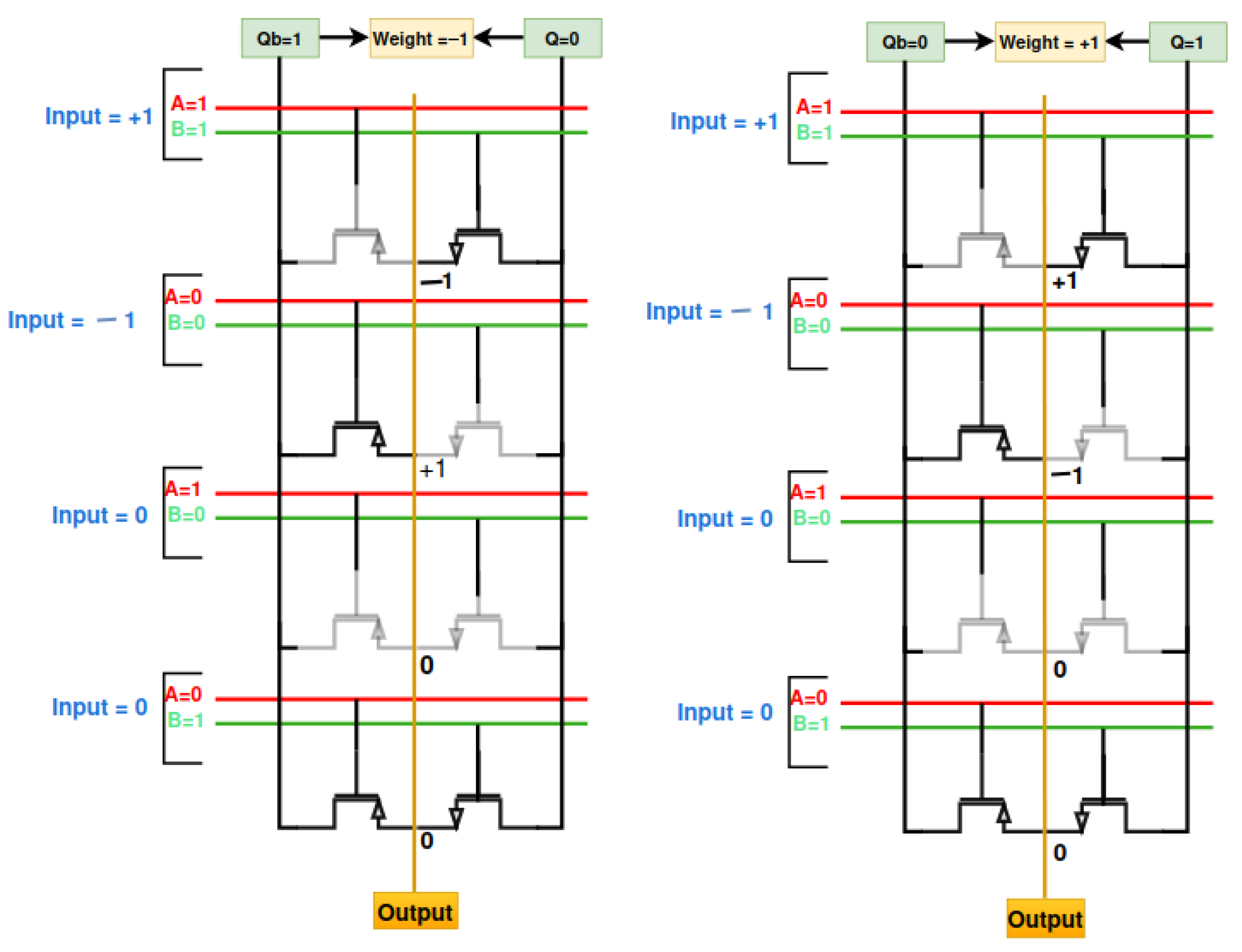
In the proposed design (
Figure 5), the PTL-based ternary XNOR gate is integrated directly within the SRAM cell [
15]. The stored values
Q and
serve as the ternary
weight information. Two control inputs,
A and
B, determine which pass-transistor paths become active during computation, thereby steering the output node toward one of the three ternary voltage levels. The logic mapping between the applied input and the stored weight is summarized in
Table 1 [
16].
The ternary XNOR operation is essential for arithmetic, correlation, and comparison tasks. When embedded directly within the memory array, this operation enables efficient compute-in-memory (CIM) execution, significantly reducing data movement, latency, and power consumption. Such ternary XNOR-in-SRAM implementations are particularly beneficial for AI and machine learning workloads that require fast and energy-efficient multiply–accumulate (MAC) operations [
17].
In our architecture, the stored data define the weight value:
When and , the weight is .
When and , the weight is .
Figure 5 illustrates how the PTL network computes the XNOR output for different ternary inputs. Depending on the combination of the applied input and the stored weight, the pass transistors direct the output to one of the ternary voltage levels corresponding to
, 0, or
. The resulting ternary output values for each input–weight pair are presented in
Table 1.
Below,
Table 1 summarizes the pass transistor logic operation.
The sizes of CNFET and GAAFET transistors in the SRAM cell are in
Table 2. Proper transistor sizing is critical to balancing this design’s speed, power, and area, particularly in subthreshold regions where achieving high yields can be challenging [
18,
19].
4. Proposed CIM Design
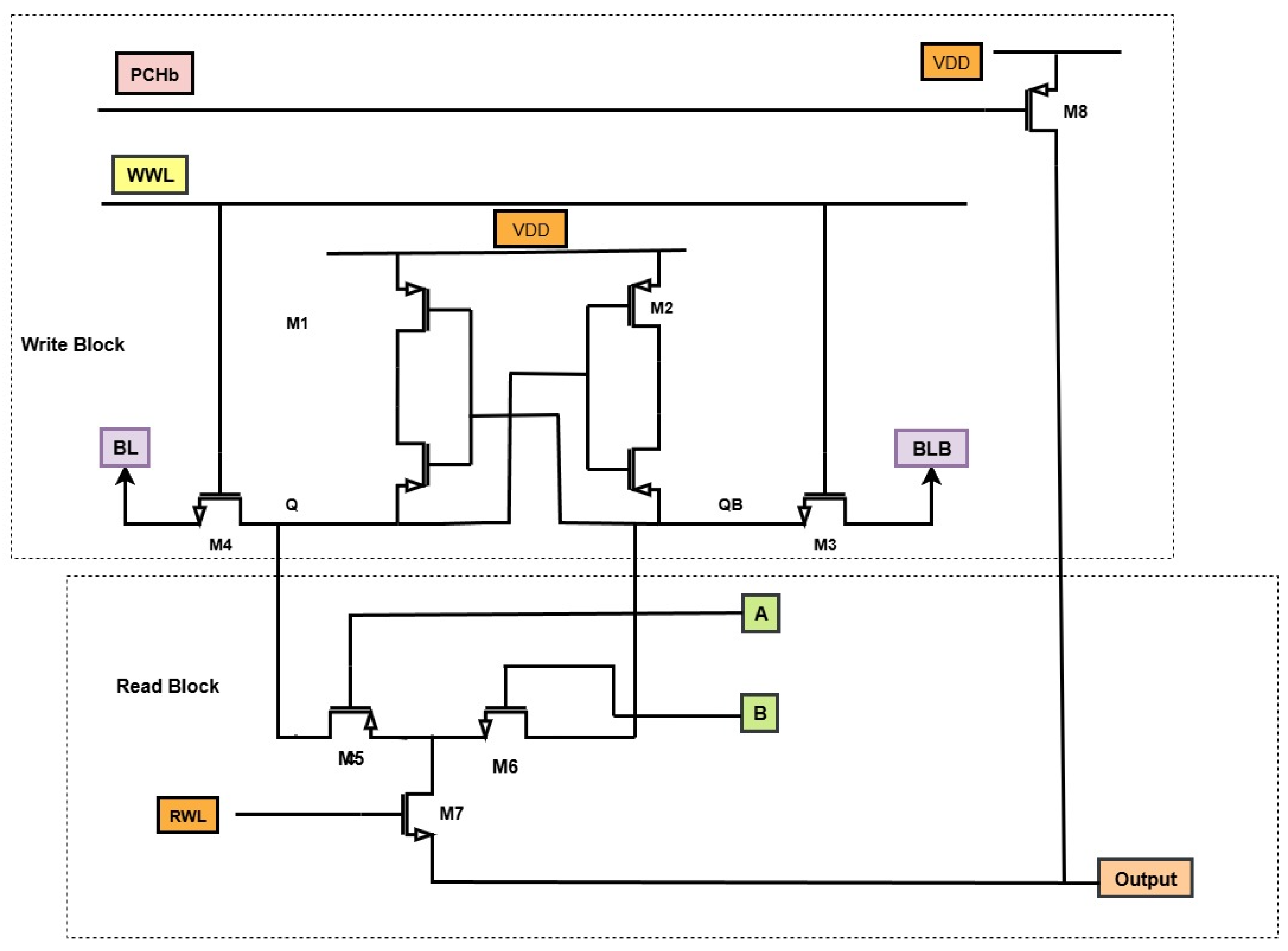
The proposed sense-amplifier embedded (SE) ternary 9T SRAM cell for computing-in-memory (CIM) is illustrated in
Figure 6. The architecture is divided into two major functional blocks: the
write block and the
read block. This separation enables improved read stability, reduced power consumption, and more efficient ternary logic implementation than conventional binary SRAM cells.
4.1. Write Block
The write block consists of cross-coupled inverters formed by transistors and , which act as the storage element of the SRAM cell. Access transistors and are controlled by the write word line (WWL) and are connected to the bit-line pair (BL and BLB). During a write operation, WWL is asserted, enabling the bit-lines to drive nodes Q and into the desired logic states.
In the ternary configuration, three distinct voltage levels are defined to represent logic states (−1, 0, and +1). The stability of these states is maintained through the positive feedback mechanism of the cross-coupled inverters. Additionally, the precharge transistor , controlled by the precharge signal (PCHb), ensures proper initialization of the bit-lines before each operation. This enhances write operation reliability and reduces dynamic power consumption.
4.2. Read Block
The read operation is isolated from the write block to minimize read disturb, which is a common challenge in multi-valued SRAM cells. The dedicated read block is composed of transistors , , and . The read word line (RWL) controls transistor , which acts as the enabling switch for the read operation.
When RWL is activated, the stored data at nodes A and B (derived from Q and ) is transferred through the read stack (–) to the output node. This ensures that the stored value is sensed without disturbing the cross-coupled inverters’ internal state. The output voltage corresponds to one of the three logic states, making the cell compatible with ternary CIM operations.
4.3. Sense Amplifier Embedding
The integration of a sense amplifier in the architecture improves the detection of ternary voltage levels, especially under process, voltage, and temperature (PVT) variations. By embedding the sense amplifier, slight differences in ternary states can be amplified, reducing sensing delay and improving read accuracy. This design choice contributes significantly to the energy efficiency and robustness of the proposed CIM cell.
4.4. Advantages of the Proposed Design
The separation of write and read paths in the 9T ternary SRAM cell offers multiple advantages:
Improved Read Stability: Isolating the read path prevents storage node disturbance during read operations.
Low-Power Operation: Precharging (via ) and selective enabling of word lines minimize unnecessary switching activity.
Support for CIM: The ternary storage mechanism directly supports multi-valued logic computations within the memory, enabling higher data density and reduced interconnect complexity.
Technology Compatibility: The design can be implemented using CNFET, GAAFET, or a hybrid CNFET-GAAFET technology, leveraging the unique low-power and high-performance characteristics of emerging devices.
Thus, the proposed SE-based ternary 9T SRAM cell provides a scalable and energy-efficient solution for computing-in-memory architectures. It combines the density benefits of ternary logic with the robustness of sense-amplifier embedding, making it suitable for future low-power computing platforms.
5. Results
5.1. Power Results
The SRAM architectures were simulated using Synopsys HSPICE 2012 to assess their performance under all four possible input conditions. Ternary weights of +1 (1.1 V), 0 (0.45 V), and −1 (0 V) were applied at room temperature (27 °C) with minimum-sized transistors. To ensure accurate representation of each circuit, individual .sp files were developed according to the original and proposed design specifications. Each simulation generated detailed output data, including waveform plots and HSPICE measurement reports that captured power consumption and delay for every operation. Average dynamic power was calculated over a 4 ns interval. Prior to each operation, the bitlines were precharged, input signals were toggled at 1 ns intervals, and leakage power was incorporated into the total power measurements.
The power consumption of each design, expressed in microwatts, for all input circumstances and weight applications, is displayed in
Table 3.
When compared to binary multiplication with +1 or −1, multiplication with zero inputs dramatically increases power consumption, according to the comprehensive power consumption analysis displayed in
Table 3. Because the zero states result in steady RBL conditions with no switching and unnecessary power retention, power consumption increases. By controlling switching activity, the binary operations with weights +1 and −1, on the other hand, display discharge and charge states in the RBL, resulting in more effective power utilization. The fact that dynamic switching leads to lower cumulative power compared to idle or stable states associated with zero input multiplications is a crucial feature of binary-weighted processes, as this finding demonstrates. From
Table 4, we can see that our three designs resulted in a power reduction of about
70% on average, compared to the original [
12].
5.2. Delay Results
The delay observed over all operations (measured in picoseconds) is recorded in
Table 5, which includes four input states with weights of +1 and −1.
Delay comparison of different states as shown in
Table 6—summarizes the total delay across all input states with weights of +1 and −1, enabling a clear comparison of delay characteristics between the original and proposed designs (measured in nanoseconds).
6. Discussion
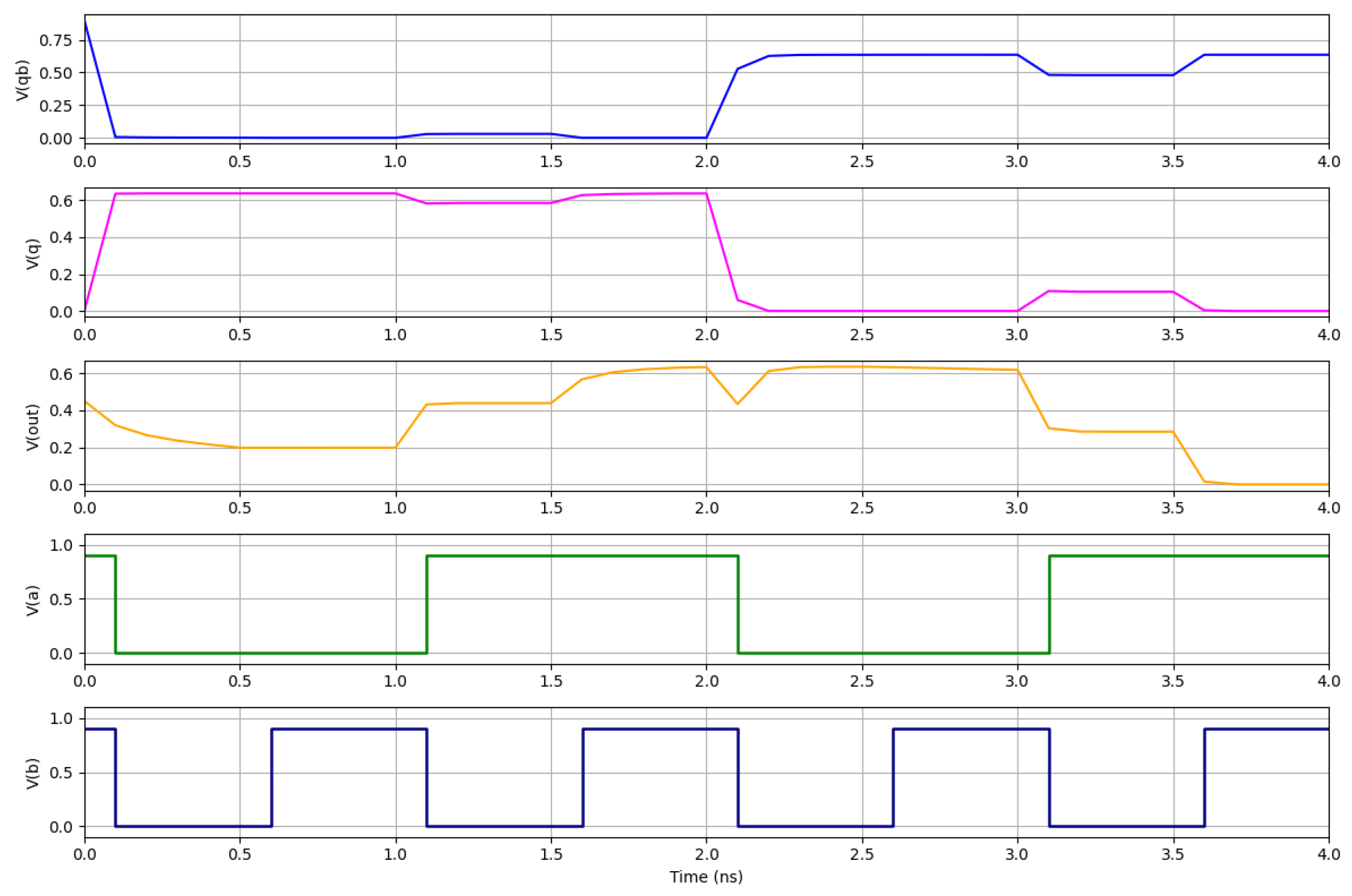
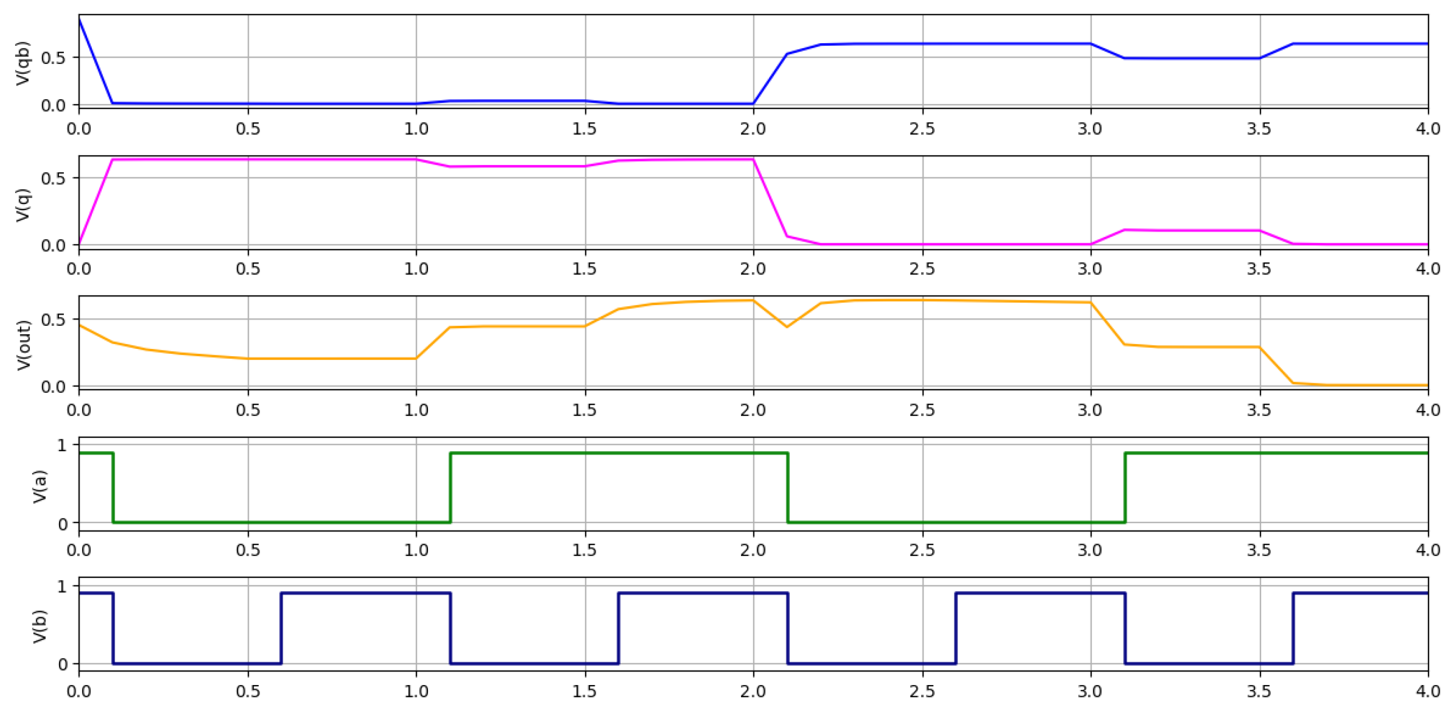
Figure 7 represents the waveform of the reference circuit.
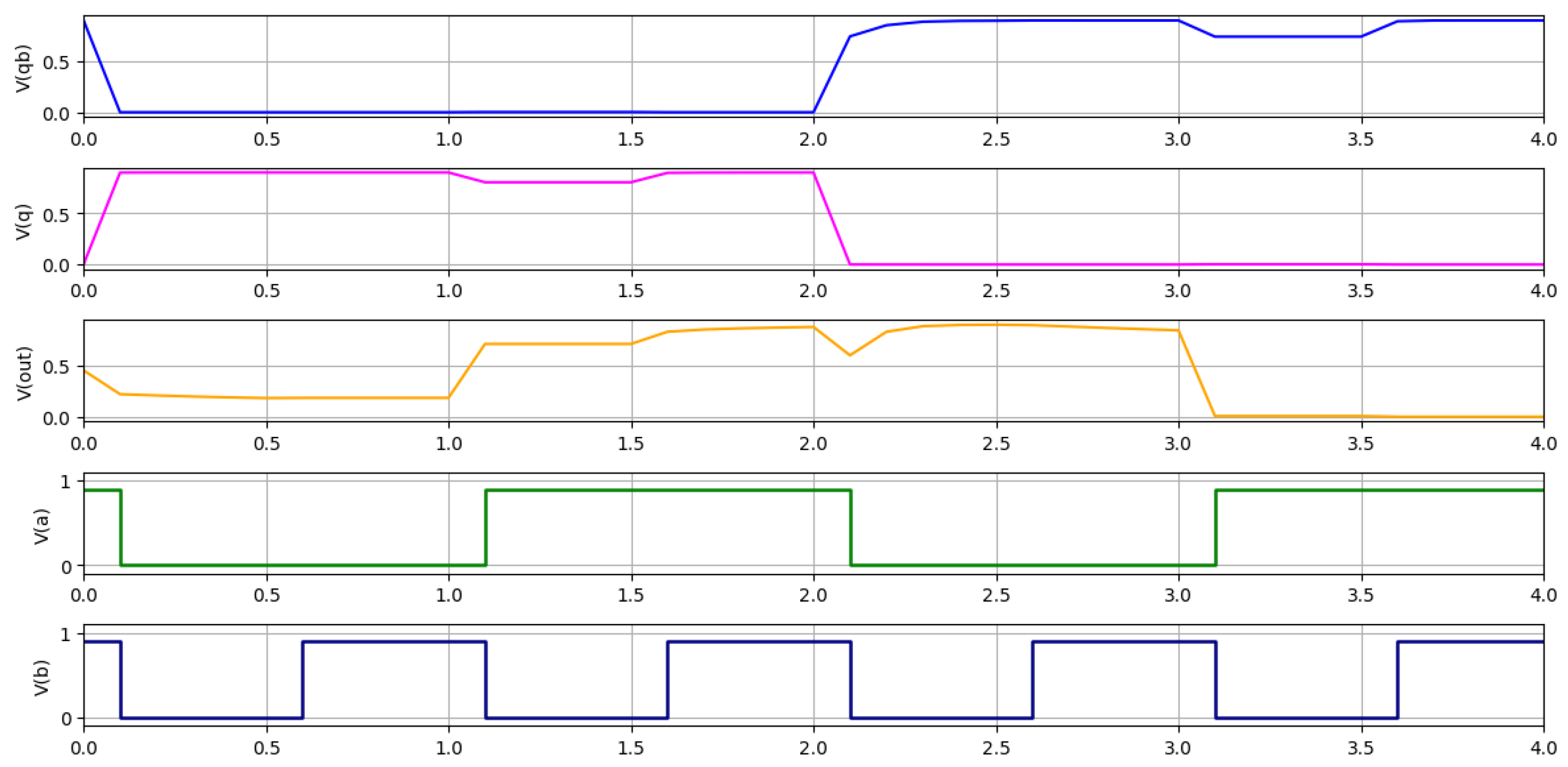
Figure 8 and
Figure 9 represent the behavior of a Compute-in-Memory (CIM) cell implemented using two different transistor technologies: CNFET (Carbon Nanotube Field-Effect Transistor) and GAAFET (Gate-All-Around FET). Each plot displays five key signals over a 4ns window—V(qb), V(q), V(out), V(a), and V(b)—to evaluate how the internal storage nodes (q and qb), the analog output node (out), and the input stimuli behave under identical conditions across the two devices.
Both the CNFET and GAAFET simulations apply the same input signals: V(a) toggles every 1 ns and V(b) switches every 0.5 ns. This ensures that any observed difference in behavior is due to the device physics rather than variations in test conditions. The internal nodes q and qb flip at approximately 2 ns and 3 ns in both plots, representing stored weights switching from +1 to −1 and back again. This weight flipping is essential for triggering different output responses based on the XNOR-style CIM operation.
The most important distinction lies in the behavior of the output voltage V(out), which reflects the cell’s analog accumulation and discharge characteristics. In the CNFET plot in
Figure 8, V(out) shows a gradual and relatively smooth change in amplitude between approximately 0.3 V and 0.6 V. Its transitions are slower, and small ripples can be observed around 2.1 ns. This suggests that the CNFET-based cell has a weaker drive strength or higher internal resistance and capacitance, leading to slower switching behavior.
In contrast, the GAAFET-based simulation in
Figure 9 exhibits a much sharper and cleaner response in V(out). The output rises more quickly and falls more steeply at key transition points, particularly around the 3 ns mark, where the output drops sharply from around 0.5 V to below 0.1 V. This indicates that GAAFETs offer superior switching characteristics, including higher drive current and better gate control, resulting in faster and more accurate analog accumulation behavior within the CIM cell.
In summary, although the input conditions and weight transitions are identical in both simulations, the GAAFET-based CIM cell demonstrates significantly better dynamic response than its CNFET counterpart. Its output transitions are faster, cleaner, and more decisive—making it more suitable for high-performance or real-time CIM applications. The CNFET cell, while functional, may face limitations in terms of speed and output sharpness, especially in scaled or low-voltage regimes. The present work validates CIM functionality at the single-cell level. Full array-level evaluation—including wordline/bitline parasitics, multi-cell MAC operations, and energy-per-row computation—is left for future work, as it requires large-scale device–circuit co-simulation.
7. Conclusions
This study establishes a low-power CNFET and GAAFET ternary 9T SRAM as a promising solution for computing-in-memory (CIM) applications. By combining the excellent gate controllability of GAAFETs with the high carrier mobility of CNFETs, the proposed design demonstrates enhanced stability, reduced power consumption, and improved delay performance over traditional CMOS-based SRAM cells. Simulation results showed that the CNFET-based approach achieved an outstanding 99.95% improvement over the original circuit, whereas the GAAFET-based design provided a 20.628% improvement. These results confirm that while GAAFET integration enhances electrostatic control and scalability, CNFET technology plays a more dominant role in delivering significant performance and power gains. The ternary logic implementation further contributes to higher storage density and reduced interconnect overhead, which are vital for energy-efficient and scalable CIM architectures.
Overall, the CNFET and GAAFET SRAM cell effectively addresses the challenges of nanoscale memory design, balancing the advantages of both technologies to support efficient logic-in-memory operations. The superior results of CNFET highlight its potential as the primary driver of future low-power architectures, while GAAFET offers complementary benefits in device scaling and leakage control. Future research on device-level co-optimization, variability analysis, and large-scale integration will be essential to validate and extend the applicability of this approach in practical CIM systems.
Author Contributions
Conceptualization, data curation, formal analysis, investigation, methodology, validation, A.A.P., S.S.D.; writing—original draft, writing—review and editing, Y.A.S., A.G.; supervision, funding acquisition, project administration, K.K.C. All authors have read and agreed to the published version of the manuscript.
Funding
This work was supported by the Korea Planning & Evaluation Institute of Industrial Technology (KEIT) grant funded by the Korea government (MOTIE) (No. RS-2024-00432265, Development of an embedded AI controller to determine road surface conditions).
Data Availability Statement
Data are contained within the article.
Acknowledgments
We thank our colleagues from KETI and KEIT, who provided insight and expertise, which greatly assisted the research and improved the manuscript.
Conflicts of Interest
The authors declare no conflicts of interest.
Abbreviations
The following abbreviations are used in this manuscript:
| AI | Artificial Intelligence |
| CNN | Convolutional Neural Network |
| DNN | Deep Neural Network |
| TBN | Ternary Binary Neural Network |
| MAC | Multiply and Accumulate |
| CIM | Compute-In-Memory |
| SRAM | Static Random Access Memory |
| ADC | Analog-to-Digital Converter |
| DAC | Digital-to-Analog Converter |
| XNOR | Exclusive-NOR |
| PTL | Pass Transistor Logic |
| PLNA | P-Latch N-Access |
| NLPA | N-Latch P-Access |
| SE | Single-Ended |
References
- Hinton, G.; Deng, L.; Yu, D.; Dahl, G.E.; Mohamed, A.-r.; Jaitly, N.; Senior, A.; Vanhoucke, V.; Nguyen, P.; Sainath, T.N.; et al. Deep neural networks for acoustic modeling in speech recognition: The shared views of four research groups. IEEE Signal Process. Mag. 2012, 29, 82–97. [Google Scholar] [CrossRef]
- Taigman, Y.; Yang, M.; Ranzato, M.A.; Wolf, L. DeepFace: Closing the gap to human-level performance in face verification. In Proceedings of the 2014 IEEE Conference on Computer Vision and Pattern Recognition, Zurich, Switzerland, 6–12 September 2014; pp. 1701–1708. [Google Scholar] [CrossRef]
- Fang, W.; Wang, L.; Ren, P. Tinier-YOLO: A real-time object detection method for constrained environments. IEEE Access 2020, 8, 1935–1944. [Google Scholar] [CrossRef]
- Alemdar, H.; Leroy, V.; Prost-Boucle, A.; Pétrot, F. Ternary neural networks for resource-efficient AI applications. In Proceedings of the 2017 International Joint Conference on Neural Networks (IJCNN), Anchorage, AK, USA, 14–19 May 2017; pp. 2547–2554. [Google Scholar] [CrossRef]
- Song, T.; Jung, J.; Rim, W.; Kim, H. A 7nm FinFET SRAM using EUV lithography with dual write-driver-assist circuitry for low-voltage applications. In Proceedings of the 2018 IEEE International Solid-State Circuits Conference (ISSCC), San Francisco, CA, USA, 11–15 February 2018. [Google Scholar] [CrossRef]
- Lu, A.; Peng, X.; Luo, Y.; Yu, S. Benchmark of the compute-in-memory based DNN accelerator with area constraint. IEEE Trans. Very Large Scale Integr. (Vlsi) Syst. 2020, 28, 1945–1952. [Google Scholar] [CrossRef]
- Si, X.; Khwa, W.-S.; Chen, J.-J.; Li, J.-F.; Sun, X.; Liu, R.; Yu, S.; Yamauchi, H.; Li, Q.; Chang, M.-F. A dual-split 6T SRAM-based computing-in-memory unit-macro with fully parallel product-sum operation for binarized DNN edge processors. IEEE Trans. Circuits Syst. Regul. Pap. 2019, 66, 4172–4185. [Google Scholar] [CrossRef]
- Castro, V.D.; Marcos, E.; Vara, J.M. Applying CIM-to-PIM model transformations for the service-oriented development of information systems. Inf. Softw. Technol. 2010, 52, 1295–1311. [Google Scholar] [CrossRef]
- Alnatsheh, N.; Youngbae, K.; Jaeik, C.; Kyuwon, K.C. A Novel 8T XNOR-SRAM: Computing-in-Memory Design for Binary/Ternary Deep Neural Networks. Electronics 2023, 12, 877. [Google Scholar] [CrossRef]
- Youngbae, K.; Patel, S.; Kim, H.; Yadav, N.; Choi, K.K. Ultra-Low Power and High-Throughput SRAM Design to Enhance AI Computing Ability in Autonomous Vehicles. Electronics 2021, 10, 256. [Google Scholar] [CrossRef]
- Youngbae, K.; Li, S.; Yadav, N.; Choi, K.K. A Novel Ultra-Low Power 8T SRAM-Based Compute-in-Memory Design for Binary Neural Networks. Electronics 2021, 10, 2181. [Google Scholar] [CrossRef]
- Lee, S.; Kim, Y. Low power ternary XNOR using 10T SRAM for in-memory computing. In Proceedings of the 19th International SoC Design Conference (ISOCC), Gangneung-si, Republic Korea, 19–22 October 2022; pp. 352–353. [Google Scholar] [CrossRef]
- Yin, S.; Jiang, Z.; Seo, J.-S.; Seok, M. XNOR-SRAM: In-memory computing SRAM macro for binary/ternary deep neural networks. IEEE J.-Solid-State Circuits 2020, 55, 1733–1743. [Google Scholar] [CrossRef]
- Biswas, A.; Chandrakasan, A.P. CONV-SRAM: An energy-efficient SRAM with in-memory dot-product computation for low-power convolutional neural networks. IEEE J.-Solid-State Circuits 2019, 54, 217–230. [Google Scholar] [CrossRef]
- Almeida, R.B.; Marques, C.; Butzen, P.F.; Silva, F.; Reis, R.A.; Meinhardt, C. Analysis of 6T SRAM cell in sub-45 nm CMOS and FinFET technologies. Microelectron. Reliab. 2018, 88, 196–202. [Google Scholar] [CrossRef]
- Mohita Newar, T.; Roy, T.; Chowdhury, J.; Das, J.K. Design and stability analysis of CNTFET based SRAM cell. In Proceedings of the IEEE Students’ Conference on Electrical, Electronics and Computer Science (SCEECS), Bhopal, India, 5–6 March 2016; pp. 1–5. [Google Scholar] [CrossRef]
- Dhare, V.; Mehta, U.; Bhatasana, P.; Parmar, C.; Patel, R. Design of carbon nanotube field effect transistor based random access memory. In Proceedings of the 10th International Conference on Applied System Innovation (ICASI), Kyoto, Japan, 17–21 April 2024; pp. 374–376. [Google Scholar] [CrossRef]
- Wang, L.; Shafaei, A.; Pedram, M. Gate-all-around FET based 6T SRAM design using a device-circuit co-optimization framework. In Proceedings of the IEEE 60th International Midwest Symposium on Circuits and Systems (MWSCAS), Boston, MA, USA, 6–9 August 2017; pp. 1113–1116. [Google Scholar] [CrossRef]
- Dabre, S.R.; Soni, D.; Saha, S. Design evaluation and performance prediction of different SRAM cell topologies through inverter optimization for the 5nm technology node using GAA CNTFETs. In Proceedings of the IEEE Silchar Subsection Conference (SILCON), Silchar, India, 3–5 November 2023; pp. 1–6. [Google Scholar] [CrossRef]
| Disclaimer/Publisher’s Note: The statements, opinions and data contained in all publications are solely those of the individual author(s) and contributor(s) and not of MDPI and/or the editor(s). MDPI and/or the editor(s) disclaim responsibility for any injury to people or property resulting from any ideas, methods, instructions or products referred to in the content. |
