Article

A 2.4 GHz CMOS Pulse-Mode Transmitter for RF Body-Contouring Device Applications

1
Department of Electronic Convergence Engineering, Kwangwoon University, Seoul 01897, Republic of Korea
2
Department of Semiconductor Systems Engineering, Kwangwoon University, Seoul 01897, Republic of Korea
*
Author to whom correspondence should be addressed.
Electronics 2025, 14(24), 4826; https://doi.org/10.3390/electronics14244826
Submission received: 14 November 2025 / Revised: 3 December 2025 / Accepted: 4 December 2025 / Published: 8 December 2025
(This article belongs to the Special Issue Modern Circuits and Systems Technologies (MOCAST 2024))

Abstract

Body-contouring devices deliver controlled thermal energy to treat cellulite, reduce localized fat, and improve skin elasticity. Since the thermal effect is closely related to the delivered RF output power, precise control of the output power is critical for both efficacy and safety. In this study, we propose a 2.4 GHz CMOS pulse-mode transmitter for body-contouring device applications, featuring precise control of the average power delivered to the body. The transmitter comprises a fully integrated phase-locked loop (PLL) synthesizer, pulse modulator (PM), and 10 mW power amplifier (PA). It is fabricated in a 65 nm CMOS with a compact die area of 3.75 mm2. The PA provides four-level continuous-mode output control from −0.3 dBm to 11.1 dBm, and the PM performs programmable PA switching for pulse-mode operation of the PA with a wide range of pulse rates and duty ratios. By combining the continuous-mode output power control and pulse-mode on–off time regulation, the average output power delivered to the skin is finely controlled, managing the delivered power within a safe skin temperature below 65 °C. The PLL loop filter is fully integrated with a wide programmability, improving the form factor and bill of materials for the target devices. Measurement results confirm that the designed transmitter can accurately control both the average output power and pulse profile across the 2.4 GHz ISM band, demonstrating its suitability for compact home-use RF body-contouring devices.

1. Introduction

Body contouring refers to the treatment of cellulite, localized adiposity, and skin laxity for improving the shape of a specific body area. Body contouring can be performed in either an invasive or noninvasive manner. The invasive procedures include surgery, incisions, and injections, which directly access subcutaneous tissues. The noninvasive procedures apply external energy to the body within non-skin-damaging safe limits. The noninvasive approaches are gaining more attention from research and marketing areas because of their advantages of no patient pain, low recovery time, low cost, low risk, and so forth [1].
Among various noninvasive approaches, radio frequency (RF) is known to effectively reduce skin laxity and localized adiposity, and its application is expanding across a wide range of body-contouring devices [2,3,4,5,6,7,8]. Commercially available devices such as Oligio (Won Tech Co., Daejeon, Republic of Korea) [4] and Onda Plus (DEKA Co., Calenzano, Italy) [5,6,7,8] are found to be clinically effective and safe.
In RF body-contouring devices, the RF energy is delivered to a target tissue layer to create thermal energy. The primary principle of thermal energy generation within the tissue depends on the applied RF frequency. At frequencies below 6.78 MHz, RF energy is delivered via an electrode that creates an electric field within the tissue. The dermis, which has a higher water content than the epidermis and subcutaneous fat layers, allows for concentrated current flow, leading to Joule heating. This localized thermal effect promotes collagen regeneration and leads to skin tightening [2,3]. In [4], they reported that the monopolar RF signal at 6.78 MHz with a maximum power of 400 W successfully generated deep-tissue heating (about 40–60 °C) and found it to be effective and clinically safe for the skin tightening and contouring purpose. Meanwhile, because most of this energy is absorbed by the dermal layer, the effect of fat reduction is also found to be rather limited [2].
In contrast, RF energy in the 2.4–2.5 GHz industrial, scientific, and medical (ISM) band is delivered via an antenna that is designed to create an electric field inside the target tissue. It has been reported that 2.4 GHz 20–80 W RF energy exposure in 1 min increases the skin temperature to 45–65 °C, leading to effective skin tightening within a safe limit [9]. The 2.4 GHz RF energy induces dielectric heating in a localized tissue region. In this frequency, the resistance of the epidermis and dermis decreases, reducing the energy loss, whereas the power delivery is higher in the subcutaneous fat layer [10], leading to more effective fat cell reduction than a few MHz [5,6,7,8]. This is because the energy is effectively absorbed by adipocytes, owing to the high power loss density [10]. It leads to more effective heat generation in the subcutaneous layer. The generated heat induces metabolic lipolysis, leading to a reduction in subcutaneous adipose tissues [5,7]. Furthermore, interstitial collagen fibers within the septa can be heated directly, leading to collagen denaturation and fibroblast activation, thereby improving skin laxity [6,8]. This mechanism promotes simultaneous fat reduction and skin laxity improvement; therefore, the 2.4 GHz ISM band is proven to be useful in body-contouring devices [5,6,7,8] as long as the RF energy is maintained within the skin-safe limit.
When RF body-contouring devices generate heat in the skin tissue, their associated risks must be properly managed to ensure user safety. The skin temperature range for safe and simultaneously effective skin tightening is known to be 45–65 °C [9]. These considerations are critical, and the design must comply with the requirements of the International Electrotechnical Commission (IEC) 60601-2-2 medical electrical equipment standard [11]. To avoid undesirable overheating, commercially available 2.4 GHz body-contouring devices usually employ a skin temperature probe and cooling systems [5,6,7,8]. But, at the same time, the average RF output power delivered to the skin must be precisely controlled to remain within the skin-safe limit. The dielectric properties of the human skin (for example, permittivity) vary with the water content, thickness, body site, and skin type, which can lead to different amounts of energy delivered to the subcutaneous fat layer [12]. Hence, the device’s output energy needs to be flexibly controlled, depending on the skin conditions and treatment objectives, so that the skin temperature is maintained within the safe limit of 45–65 °C.
Since the thermal energy delivered by RF body-contouring devices is proportional to the transmitter’s output power and exposure time, a precise and wide-range control of these parameters is needed. The pulse-mode operation of RF transmitters is widely employed for medical devices because of the flexible controllability [13]. It periodically provides rest intervals in between intensive RF electrical stimulations, providing sufficient time for heat dissipation and skin cooling, whereas continuous-wave operation is very vulnerable to unwanted side effects, such as skin burns, nerve tissue damage, and pain [14]. Pulse-mode operation is found to significantly reduce the risk of heat-induced nerve injury [15].
Recent works show that home use of body-contouring devices is rapidly increasing compared with traditional clinic use [16,17,18]. For a home-use device, its form factor and power consumption are crucial and demanding; therefore, an area/power-efficient hardware implementation is imperative. The control of critical parameters such as the output power and pulse parameters by a single complementary metal-oxide semiconductor (CMOS) integrated circuit (IC) is, thus, required. Previous 2.4 GHz CMOS RF transmitter ICs for wireless biomedical and sensor network applications were reported in [19,20,21,22,23]. However, these 2.4 GHz transmitters only supported a simple on–off keying (OOK) modulation with a <0 dBm output power. We find that they are not suited for the RF body-contouring device applications of this work. This work requires a 2.4 GHz RF transmitter that can support a much higher output power of >+10 dBm and much more flexible pulse-mode control with a pulse rate of a few hundred Hz to kHz and a duty ratio of 10–90%.
This paper describes the design and implementation of a 2.4 GHz pulse-mode CMOS transmitter that features essential key functions required for RF body-contouring devices. The technical contributions of this work are as follows: (1) development of a CMOS pulse-mode transmitter with precise average-power control over a wide range; (2) integration of an on-chip loop filter in a PLL synthesizer for robust and stable operation under process, voltage, and temperature (PVT) variations through post-fabrication calibration; and (3) realization of an area-efficient architecture suitable for small-form-factor home-use RF body-contouring device applications.
The remainder of this paper is outlined as follows. Section 2 describes a block diagram of the proposed CMOS transmitter. Section 3 describes the circuit implementation of the proposed CMOS transmitter. Section 4 discusses the measurement results, and Section 5 highlights the main conclusions of this study.

2. CMOS Pulse-Mode RF Transmitter Architecture

Figure 1 shows the block diagram and control scheme of key parameters of the total 2.4 GHz RF body-contouring device. The total device comprises a CMOS transmitter (TX) for 2.4 GHz pulse-mode signal generation, a power amplifier module (PAM) incorporating a tens-to-hundreds of watts GaN power amplifier, and an antenna, among which this work focuses on the CMOS RFIC. The 2.4 GHz signal generated by the CMOS transmitter is amplified by the PAM, which delivers RF energy of tens to hundreds of watts to the skin layer during the pulse-on time and provides epidermal cooling during the pulse-off time.
In a typical design, the output power of the PAM should range from 20 W to 200 W [9,24]. The PAM is assumed to have a gain of 43 dB and a saturated output power of 53 dBm. Thus, the CMOS RF transmitter must drive the output power to greater than 10 dBm.
A previous biomedical study demonstrated that a 600 Hz pulse-mode signal with a 10% duty cycle effectively modulates skin inflammatory responses and heals the wound spot [25]. Although [25] did not present comprehensive results on the clinical impacts with respect to the pulse rate and duty cycle variations, their findings have guided us to select the frequency and duty cycle control range. As illustrated in Figure 1, the proposed CMOS transmitter of this work is designed to support power control from 0 dBm to 10 dBm, a pulse frequency range of 500 Hz to 3.3 kHz, and a duty cycle range of 2.5% to 97.5%.
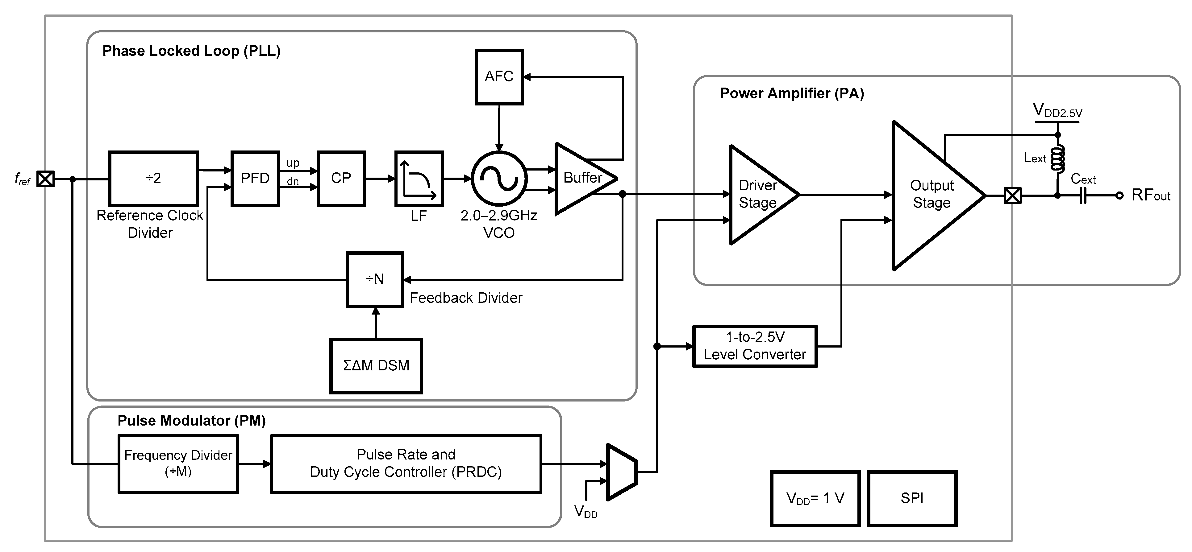
Figure 2 shows the block diagram of the proposed 2.4 GHz CMOS pulse-mode RF transmitter. The proposed transmitter consists of a phase-locked loop (PLL) synthesizer, pulse modulator (PM), and 10 mW CMOS power amplifier (PA). The supply voltage for the PLL, PM, and PA’s driver stage is 1 V, whereas the PA output stage operates from an external 2.5 V supply. This is because with 1 V, we cannot achieve the maximum output power up to +10 dBm. Both the PLL and PM share a 40 MHz reference clock. A serial peripheral interface (SPI) is used for digital state control of the chip.
The PLL is a charge-pump type-II structure with a digital delta-sigma modulator for fractional-N frequency synthesis [26,27]. The loop filter is integrated on the chip so that the external loop filter components can be eliminated and the post-fabrication calibration of the loop bandwidth can be performed. The voltage-controlled oscillator (VCO) is designed to cover a sufficiently wide tuning of 2.0–2.9 GHz in order to ensure robust coverage of the target 2.4 to 2.5 GHz ISM band.
The PA operates in pulse mode by switching the PA’s DC bias voltages via the PM signal, which converts the continuous RF signal into the pulse-mode RF signal with the wanted pulse rate and duty cycle.
The PM first divides the reference clock. The pulse rate and duty cycle controller (PRDC) then manipulates the pulse profile with the wanted pulse repetition rate and duty cycle. Since the PA output stage operates from a 2.5 V supply, the PM output signal is level-converted from 1 V to 2.5 V prior to being fed to the PA output stage. Note that the PA switches in response to the PM signal, which allows for facilitating stable and fast control of the RF output energy. If the VCO is directly switched on and off by the PM signal, it may easily cause the PLL to lose its lock temporarily, leading to serious limitations. In contrast, the periodic on–off switching of the PA in response to the PM signal enables the PLL to remain locked and ensures that power is consumed only during PA on-time, thereby improving overall power efficiency.

3. Circuit Implementation

3.1. Voltage-Controlled Oscillator (VCO)

Figure 3a shows the VCO schematic. The VCO operates at a supply voltage of 1 V with a DC bias current of 500 µA at M5. The VCO is designed in a complementary cross-coupled negative-transconductance structure [27]. The LC tank consists of a 4.92 nH tank inductor Ltank, a 105–182-fF varactor capacitor Cvar, and a 5-bit switched-capacitor bank Cbank.
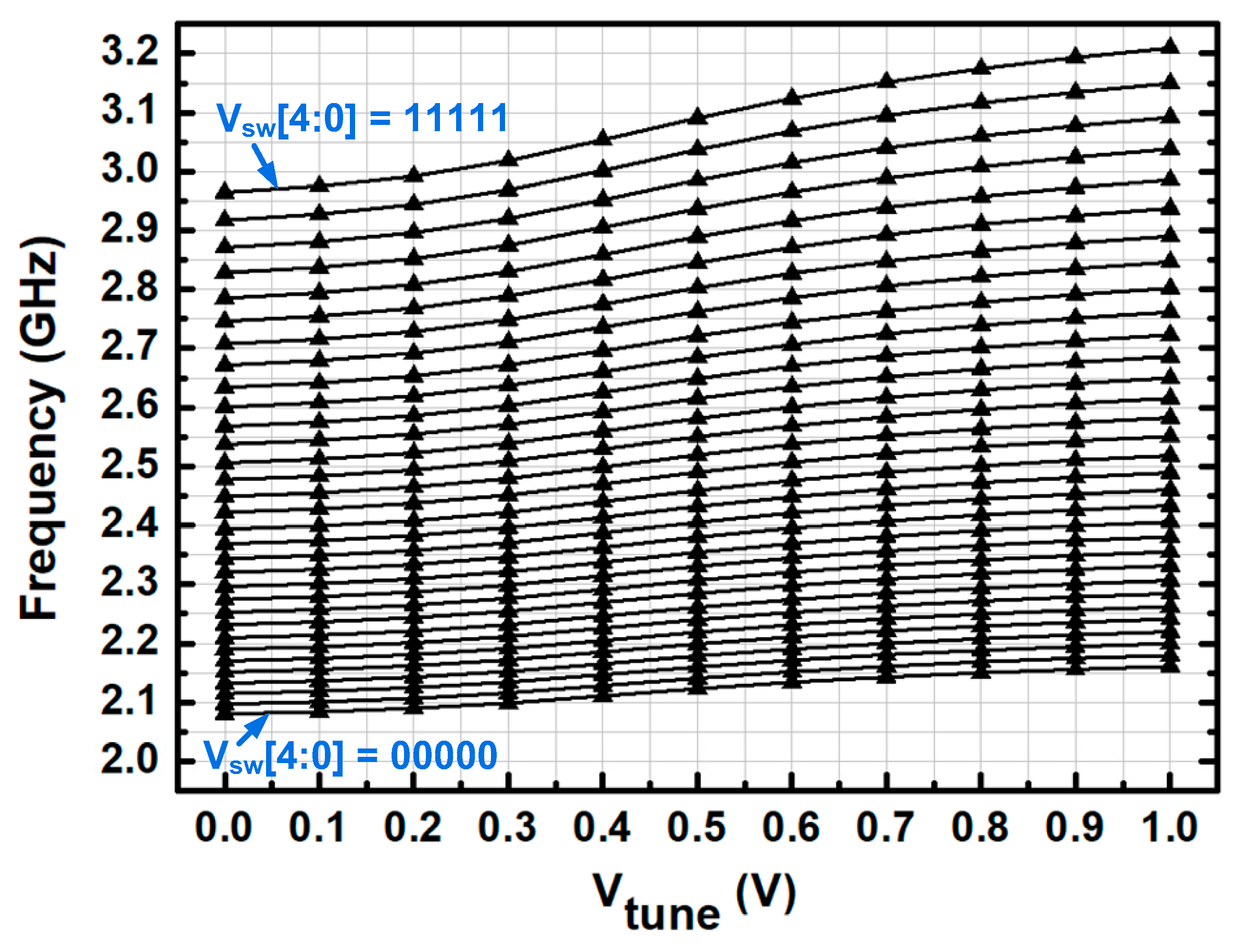
The oscillation frequency is tuned via Cvar and Cbank. It is first coarse-tuned by digitally switching the Cbank. The coarse tuning is automatically carried out by the automatic frequency calibration (AFC) shown in Figure 2. The AFC automatically finds the closest sub-band frequency tuning curve out of the 32 sub-band curves so that the final Vtune can be set as close as possible to the half VDD of 0.5 V [27]. Then, the PLL’s closed-loop locking operation via Cvar settles the output frequency to a target value.
The switched-capacitor array bank schematic is shown in Figure 3b. The total capacitance of Cbank is controlled by the 5-bit signal CB[4:0], which selectively activates the switches Msw. The switch FET Msw consists of two NFETs connected in an opposite manner, with one’s source connected to the other’s drain and vice versa. This can improve the differential symmetry of the VCO output signal. The gate and source/drain nodes are simultaneously switched in an inverted manner to reduce the off-state parasitic capacitance [26]. The 5-bit capacitor array bank is sized in a binary weighted scale from 1× to 16× with a unit Cu of 60 fF for effectively generating the 32 sub-band curves.
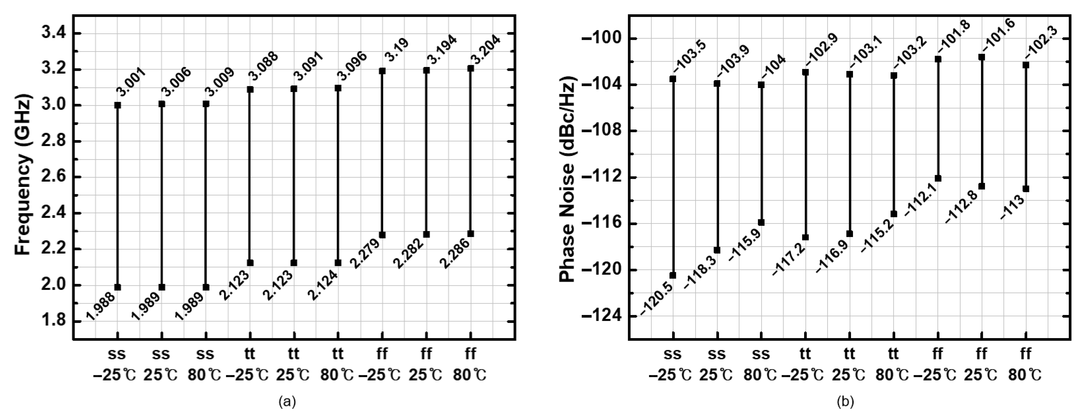
Figure 4 shows the simulation results of the VCO frequency-tuning range under a typical condition. As can be seen, the VCO frequency is tuned from 2123 MHz to 3091 MHz with 32 steps, which sufficiently covers the desired 2.4–2.5 GHz ISM band. Figure 5 investigates the frequency-tuning range and phase noise variations over the nine process and temperature corners of a fast/typical/slow process and −25/+25/+80 °C temperature conditions. The endpoint data are written in Figure 5. It is clear that over the harsh and wide PVT variations, the desired frequency tuning range of 2.4–2.5 GHz is well covered, and the phase noise is maintained at better than −101.6 dBc/Hz.

3.2. PLL and On-Chip Loop Filter

The detailed design of the PLL synthesizer has been described in the author’s previous works [26,27], where they adopted an off-chip loop filter. In this work, we integrate the loop filter inside the chip as well as make it programmable for versatile loop bandwidth calibration.
Note that the loop bandwidth influences the PLL’s locking behavior and phase noise performances [28,29]. It is generally known that a narrower loop bandwidth leads to a longer locking time and lower phase noise, and a wider loop bandwidth leads to faster locking time but worse phase noise. Thus, the loop bandwidth must be properly managed within a particular range in any harsh PVT corners. Thus, we adopt programmable resistors and capacitors on-chip in the loop filter.
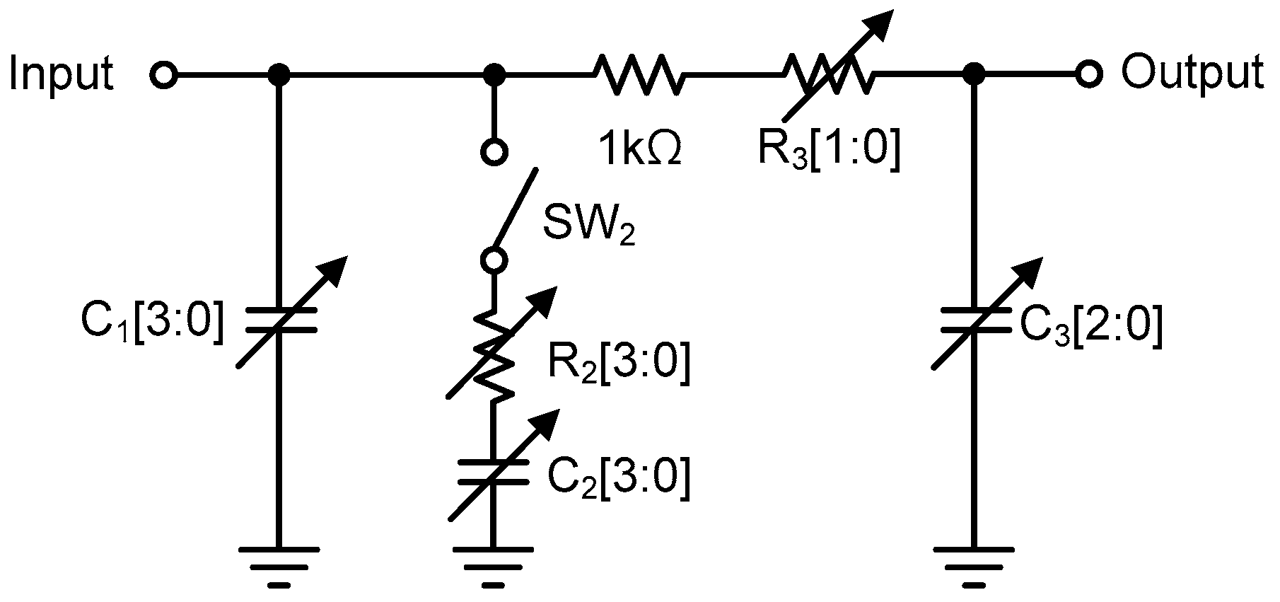
Figure 6 shows the programmable on-chip loop filter schematic. It consists of a switch, SW2, two programmable resistors, R2 and R3, and three programmable capacitors, C1, C2, and C3. SW2 either connects or disconnects R2 and C2. When SW2 is off, the on-chip loop filter can be optionally disconnected, and an off-chip loop filter can be incorporated when needed. When SW2 is on, the on-chip R2 and C2 are connected to realize the fully integrated on-chip loop filter.
In this design, the loop filter component values are optimally set for achieving the nominal loop bandwidth of 230 kHz and phase margin of 45 degrees with a given charge-pump current (100 µA), PFD comparison frequency (20 MHz), output frequency (2.4–2.5 GHz), and VCO gain Kvco (320 MHz/V).
Figure 7a shows the Kvco variations for the 32 sub-band tuning curves at the nine process and temperature corners of the fast/typical/slow process and −25/+25/+80 °C temperature conditions. Kvco is computed by taking a derivative of the frequency-tuning curves with respect to the tuning voltage Vtune. Assuming that Vtune is maintained within 0.3–0.7 V during the PLL locked condition, the maximum and minimum Kvco values are found to be 421 MHz/V and 70 MHz/V, respectively, while the typical Kvco is found to be 320 MHz/V at the typical process corner and 25 °C temperature.
The programmable on-chip resistance and capacitance values must accommodate the Kvco variations for maintaining the nominal values of the loop bandwidth and phase margin at 230 kHz and 45 degrees, respectively. The tuning ranges and steps of the RC components of the loop filter are listed in Table 1. The on-chip calibration is performed via SPI control. Figure 7b–d show the PLL loop characteristics of the closed-loop gain, open-loop gain, and the phase transfer functions, respectively, after loop filter calibration for five selected Kvco conditions of 70, 160, 250, 340, and 421 MHz. For the optimal loop filter calibration, the RC components are set as follows: C1, C2, C3, R2, and R3 are set to 30 pF, 150 pF, 12 pF, 16 kΩ, and 1 kΩ, respectively, at Kvco = 70 MHz/V; 70 pF, 350 pF, 12 pF, 7 kΩ, and 1 kΩ, respectively, at Kvco = 160 MHz/V; 100 pF, 550 pF, 12 pF, 4 kΩ, and 1 kΩ, respectively, at Kvco = 250 MHz/V; 140 pF, 750 pF, 12 pF, 3 kΩ, and 1 kΩ, respectively, at Kvco = 340 MHz/V; and 180 pF, 900 pF, 12 pF, 2 kΩ, and 1 kΩ, respectively, at Kvco = 421 MHz/V. Note that R3 and C3 do not change during the calibration because it only sets the far-out pole. After this calibration, and the Kvco of MHz, the loop bandwidth is found to be 213, 230, 233, 246, and 234 kHz when Kvco is 70, 160, 250, 340, and 421 MHz/V, respectively, which is only ±7.1% around the nominal loop bandwidth of 230 kHz. Meanwhile, the phase margin is found to be 39, 42, 44, 44, and 43 degrees when Kvco is 70, 160, 250, 340, and 421 MHz/V, respectively, in Figure 7d. Thus, the loop filter calibration successfully guarantees stable and robust locking performances for the PLL synthesizer.

3.3. Pulse Modulator (PM)

Figure 8 shows the block diagram of the PM. It consists of a frequency divider and a pulse rate and duty cycle controller (PRDC). The frequency divider accepts the 40 MHz reference clock from an external crystal oscillator and converts it to a lower internal-clock fint between 9.77 kHz and 20 MHz, depending on the division ratio M between 2 and 4094. The PRDC then modulates the pulse rate and duty cycle.
The frequency divider sets fint by HP[10:0] between 1 and 2047. On each positive edge of the input reference frequency fref, the counter value is incremented, and when it reaches the preset HP[10:0], the output is inverted. As a result, fint becomes fref divided by two times HP[10:0].
The PRDC then synthesizes the pulse to have the wanted pulse rate and duty cycle. HT[5:0] between 1 and 63 sets the number of fint cycles for the output staying high, whereas LT[5:0] between 1 and 63 sets the number of fint cycles for the output staying low. The PRDC is enabled only when HT[5:0] + LT[5:0] is greater than or equal to 3 for stable operation. Then, the PM output frequency fpm is given by
f p m = f r e f 2 · H P [ 10 : 0 ] × ( H T [ 5 : 0 ] + L T [ 5 : 0 ] )
Meanwhile, the duty cycle of the PM output, DTpm, is determined by the ratio of HT[5:0] to HT[5:0] + LT[5:0], as given by
D T p m = H T [ 5 : 0 ] H T [ 5 : 0 ] + L T [ 5 : 0 ]
Figure 9 illustrates several selected points of the possible pulse frequency fpm and duty cycle DTpm that can be generated by the PM. As shown in Figure 9, the PM can set the pulse frequency fpm in the range of 0.5–3.3 kHz, and the duty cycle DTpm in the range of 2.5–97.5%. For example, as denoted in Figure 9, when HP[10:0] is set to 600, 800, and 1000, fint is set to 33.3, 25, and 20 kHz, respectively. Then, for fint = 20 kHz with HP[10:0] = 1000, when HT[5:0] and LT[5:0] are set such that their sums are 10, 20, and 40, the fpm is set to 2 kHz, 1 kHz, and 500 Hz, respectively, and also DTpm is tuned with 10%, 5%, and 2.5% steps, respectively. Note that as the sum of HT[5:0] and LT[5:0] increases, the DTpm step decreases proportionally. For example, when the sum is 10, DTpm is adjusted in 10% increments from 10% to 90%. When the sum is 20, DTpm is adjusted in 5% increments from 5% to 95%. When the sum is 40, DTpm is adjusted in 2.5% increments from 2.5% to 97.5%.

3.4. Power Amplifier (PA)

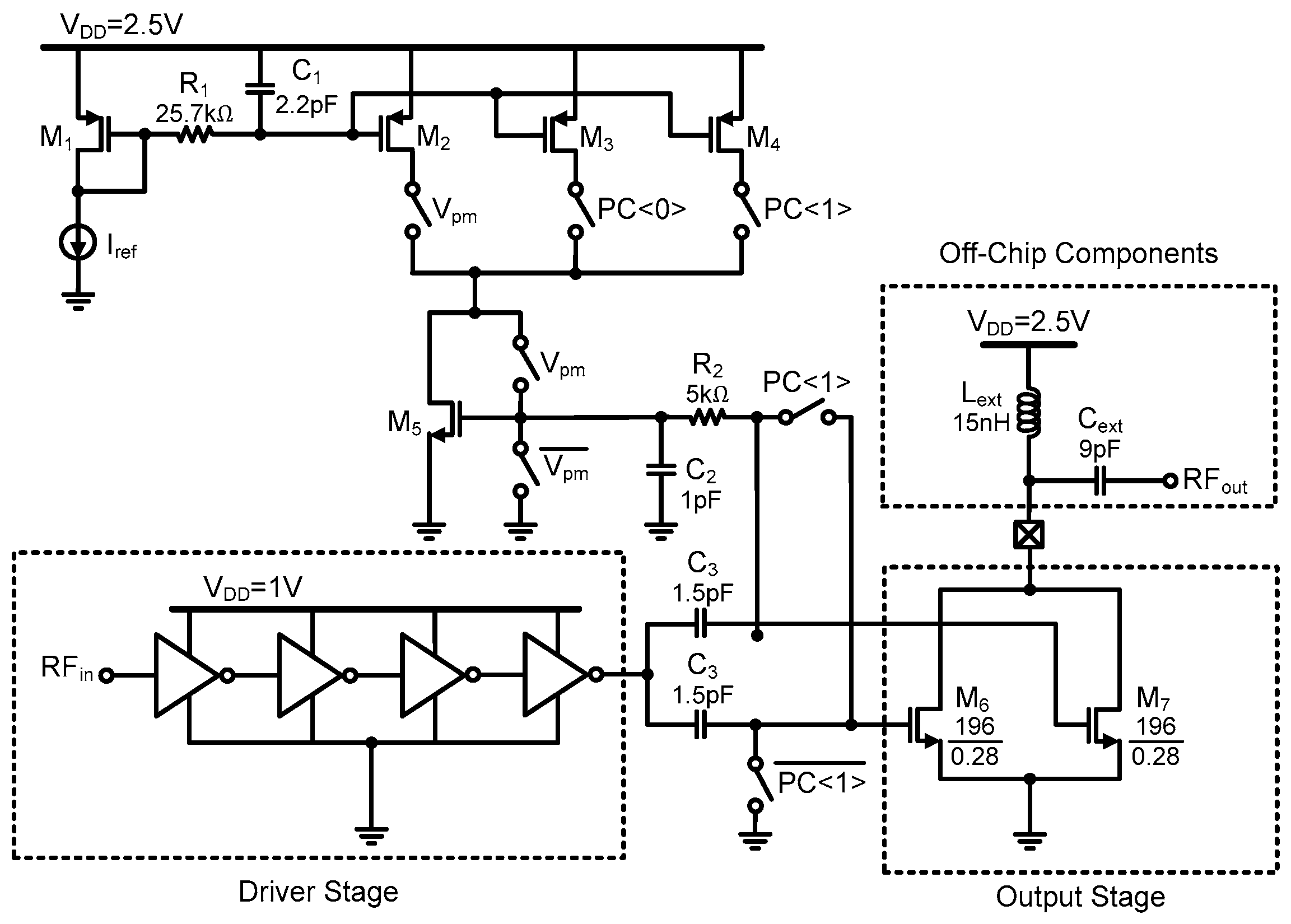
Figure 10 shows the CMOS PA circuit schematic. The PA consists of a four-stage driver stage and an output stage. The driver stage is designed in a four-stage self-biased current-reuse complementary common-source structure to generate a sufficient voltage swing with low power consumption [30]. It operates from a 1 V supply to provide a rail-to-rail swing.
The subsequent output stage comprises the common-source stage M6 and M7 with an open-drain configuration, operating from a supply voltage of 2.5 V. Note that the open-drain common-source configuration is employed for generating the required +10 mW output power, which is not possible with the internal 1 V supply.
The output stage incorporates the pulse-mode switching function as well as the continuous-mode power control function, which is carried out by utilizing the PM signal Vpm and power control digital signal PC[1:0]. When Vpm is 0, M5 is off, and the power stage is turned off. When Vpm is 1, the current-mirror M5 is enabled, and its bias current is determined by M2,3,4. When PC[1] = 0, only M7 is activated, and the lower two-step power levels are generated according to PC[0]. Meanwhile, PC[1] also turns on the PA core FET M6, which increases the effective FET width for further boosting the output power. Thus, when PC[1] = 1, M6 and M7 are both activated, and the two higher power levels are generated. As a result, the four-step power control levels of +1.4, +4.3, +9.7, and +12.3 dBm are achieved.
Figure 11 shows the simulation results of the output power and power-added efficiency against the input power. It shows that at the output power of +11 dBm, the power-added efficiency is 16.6%, and at the input power of −10 dBm, the output power is saturated to +12.3 dBm with the power-added efficiency of 21.6%. Over the temperatures of −25, +25, and +80, the simulation shows that the power gains are +24, +22.9, and +19.7 dBm, and the saturated output powers are +12.6, +12.3, and +11.8 dBm, respectively. Note that the class-A operation from an external 2.5 V supply limits the power-added efficiency to some extent; however, it is adopted to effectively realize the four-step power control.

4. Measurement Results

The proposed 2.4 GHz pulse-mode TX IC was fabricated in a 65 nm single-poly nine-metal (1P9M) RF CMOS process. Figure 12 shows a micrograph of the fabricated chip, in which the key building blocks are denoted. The die size is 1.5 mm × 2.5 mm, including 60 surrounding pads. It is housed in a 48-pin quad flat no-lead (QFN) package, for which the 48 pads are connected to the lead frames and the remaining 12 pads are connected to the bottom ground plane of the package for solid grounding.
The chip test environment is shown in Figure 13. The packaged chip is mounted on a printed circuit board (PCB) with all the external components needed for measurements mounted on the same PCB. The internal digital states of the IC are set by SPI control. The 40 MHz crystal oscillator provides the common reference clock to the IC. The TX output is measured via an SMA connector. The PA output stage operates from a 2.5 V supply and consumes 6.5, 9.6, 18.4, and 30.9 mA at the four-step power control settings, respectively. The output matching network of the PA shown in Figure 10 comprises an Lext of 15 nH and a Cext of 9 pF for 50 ohm impedance matching. The remaining part of the chip consumes 8.7 mA from a 1 V supply.
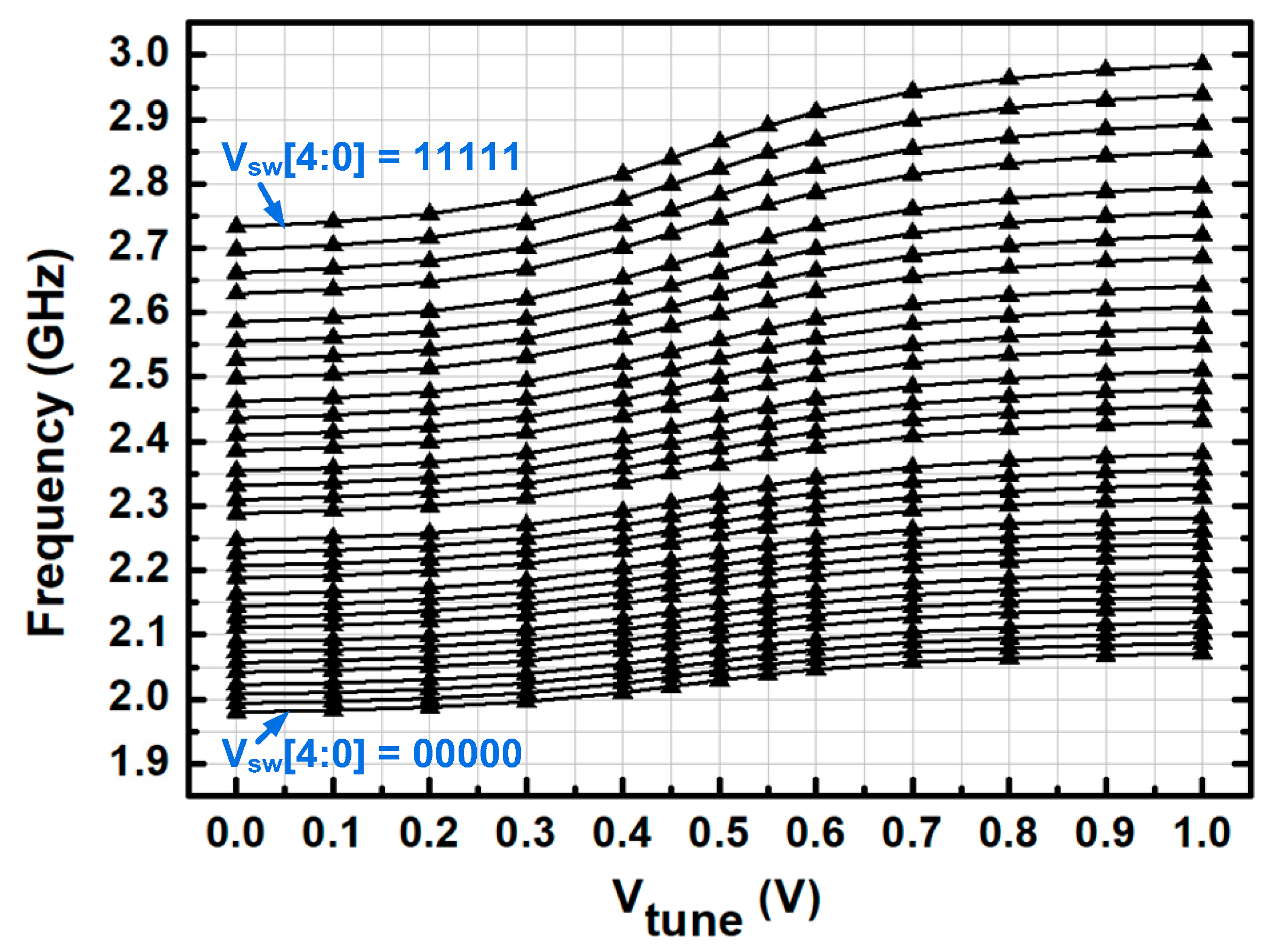
Figure 14 presents the measured results of the VCO frequency-tuning characteristics. The VCO frequency was tuned from 2030 to 2867 MHz across the 32 discrete sub-band curves at the VCO tuning voltage at Vtune of 0.5 V, which sufficiently covered the target 2.4–2.5 GHz ISM band. The tuning range was observed slightly down-shifted by 4.4–7.4% compared with the simulation results due to the layout parasitic effects. At around 2.4 GHz and a Vtune of 0.5 V, the Kvco was found to be 300–340 MHz/V, which was within the design range. The measured results agree well with the simulation results of Figure 4.
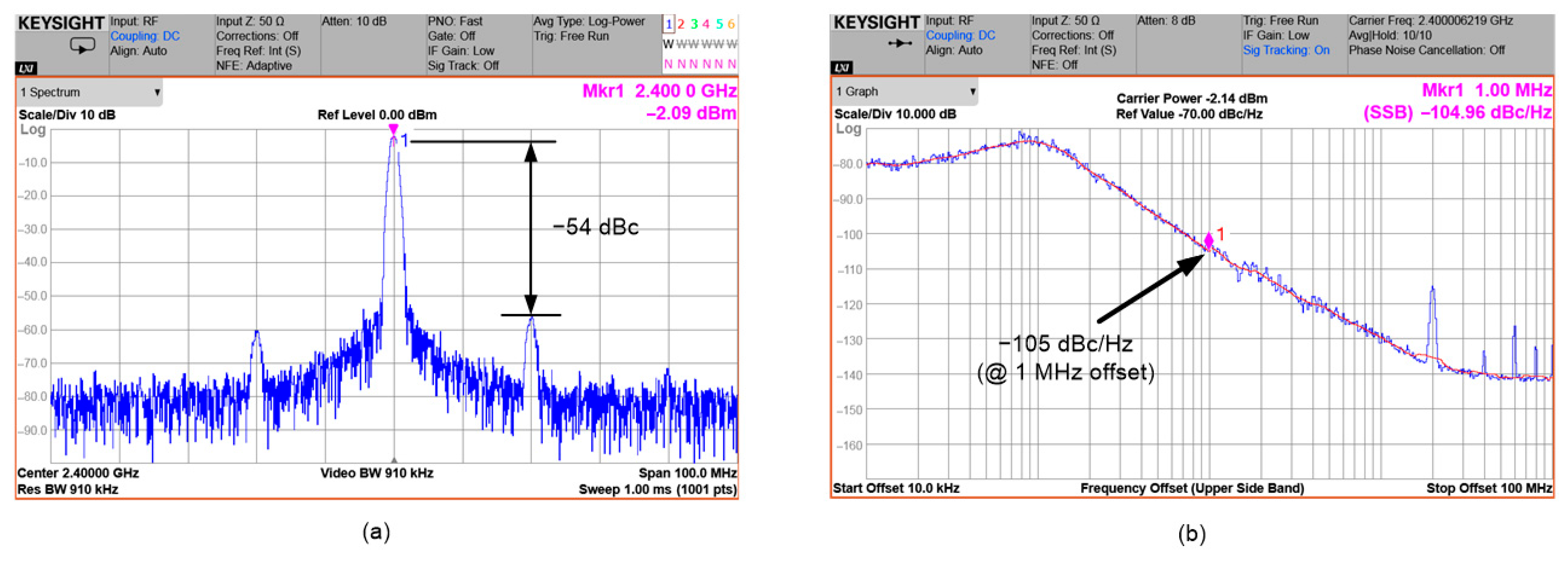
Figure 15a shows the PLL output spectrum at 2.4 GHz, and Figure 15b shows the phase noise profile. A signal analyzer (N9030B, Keysight Technologies Inc., Santa Rosa, CA, USA) was used for these measurements. In Figure 15a, the 20 MHz reference spur of −54 dBc was observed, which was because the PFD comparison frequency was 20 MHz via the reference clock divided by two in Figure 2. The modest spur level is attributed primarily to the charge pump non-idealities and also to the non-negligible ground ripple induced via the on-chip loop filter. Nevertheless, this spur level was found to be satisfactory for body-contouring device applications.
In Figure 15b, the phase noise at an offset frequency of 1 MHz is −105 dBc/Hz, which ensures sufficient spectral purity and electromagnetic interference for body-contouring devices. It was also experimentally verified that the on-chip calibration successfully maintained the loop bandwidth at 230 kHz within 10% error.
The four-step continuous-mode power control was tested, as shown in Figure 16, for which the transmitter was set to continuous mode instead of pulse mode. It was observed that the output power levels were controlled to −0.3, +3.3, +8.6, and +11.1 dBm at the power control modes 0, 1, 2, and 3, respectively, giving the total power control range of 11.4 dB. The four-step output power was found to be lower by 1–2 dB compared with the simulation results, which can be attributed to the parasitic effects of the bond wire and PCB routings. With the total power consumption of the transmitter IC (8.7 mA from 1 V and 30.9 mA from 2.5 V) at the maximum output power of +11.1 dBm, the power efficiency was found to be 14.9%.
Figure 17 shows the time-domain power control performance under the pulse-mode operation. These measurement results were obtained by using the time-domain measurement function of the signal analyzer. The RF frequency was fixed at 2.4 GHz, and measurements were performed with various pulse frequencies and duty cycles. Figure 17a shows the results at a pulse frequency of 500 Hz and a duty cycle of 10%, Figure 17b at 1000 Hz and 50%, Figure 17c at 3300 Hz and 50%, and, finally, Figure 17d at 3300 Hz and 90%. They clearly demonstrate that the transmitter IC can successfully control the pulse rate and duty cycle so that the average power delivered to the skin, as well as the cooling-off period, can be properly set, however the user wants.
In addition, since skins could be sensitive to residual emissions when the PA is off, the residual off-state output power was measured, which was found to be below −70 dBc. It proved sufficient safety for RF body-contouring devices.
Figure 18 presents the time-domain transient waveforms of the transmitter output in the pulse mode. The waveforms were captured using an digital sampling oscilloscope (Infiniium 54855A, Keysight Technologies Inc., Santa Rosa, CA, USA). Figure 18a shows the waveform measured at a pulse frequency of 500 Hz, duty cycle of 10%, and RF frequency of 2.4 GHz, whereas Figure 18b shows it at a pulse frequency of 1000 Hz and duty cycle of 50%. Figure 18c,d show the waveforms at 3300 Hz at duty cycles of 50% and 90%, respectively. These results also confirm that the proposed transmitter can effectively control the pulse rate and duty cycle.
Table 2 summarizes the measured performances of the fabricated CMOS pulse-mode TX IC and compares them with the recent 2.4 GHz CMOS transmitters for wireless biomedical and sensor network applications [19,20,21,22,23]. The device in this work supports flexible pulse modulation with a wide range of pulse rate control (0.5–3.3 kHz) and duty ratio control (2.5–97.5%), while the others support only a simple OOK modulation. The device in this work generates up to +11.1 dBm output power, while others generate much lower output power. This work embedded the fully-integrated PLL with a programmable on-chip loop filter, while others only employed a simple VCO without PLL [19,21,22,23]. The power efficiency in this work was lower than that in [19,20]. The transmitter in [19] employed a switching power amplifier and open-loop VCO frequency generation to generate a low output power of −14.1 dBm and the relaxed operating frequency accuracy, which led to a high TX efficiency. The transmitter in [20] achieved a high efficiency of 27.3% by employing a switching-mode power amplifier, whereas this work employed a class-A power amplifier, but the output power was limited to less than 0 dBm. The transmitters in [21,22,23] demonstrated an extremely low power consumption of less than 1 mW so that the output power levels were much lower (−17–−33.4 dBm), and their efficiencies were also found to be very low.

5. Conclusions

This study described the design and implementation of a 2.4 GHz CMOS pulse-mode transmitter for RF body-contouring device applications. It is implemented in a 65 nm RF CMOS process and occupies a die area of 3.75 mm2. The frequency-tuning range of 2.0–2.9 GHz is sufficient to cover the ISM band. The PLL phase noise of −105 dBc/Hz and spur level of −54 dBc ensures sufficient spectral purity. The output power control range of 11.4 dB and the wide-range PRDC can guarantee robust and flexible control of an average output power and cooling-off time. The fully integrated on-chip loop filter of the PLL reduces the external components and ensures robust and stable operation via post-fabrication on-chip calibration.
The proposed IC can be co-integrated with an external high-power amplifier and a miniature antenna to deliver a pulse-mode 2.4 GHz RF energy to the skin for body-contouring applications. The thermal safety can be guaranteed by optimally controlling the output power level, pulse frequency, and duty ratio. An auxiliary skin temperature probe and a cooling system can be employed for further safety satisfaction. Compared with previous conventional CMOS OOK transmitters, this CMOS TX IC can support very flexible pulse-mode operation, high output power, and a fully integrated PLL. Thus, it can be instrumental for low-power compact home-use RF body-contouring device applications.

Author Contributions

Conceptualization, J.J. and H.S.; methodology, J.J. and H.S.; validation, G.J., H.J., S.J., J.J., and H.S.; formal analysis, G.J., H.J., S.J., and J.J.; investigation, G.J., H.J., S.J., and H.S.; data curation, G.J., H.J., and S.J.; writing—original draft preparation, G.J. and J.J.; writing—review and editing, J.J. and H.S.; visualization, G.J. and S.J.; supervision H.S.; project administration, H.S.; funding acquisition, H.S. All authors participated in all other aspects. All authors have read and agreed to the published version of the manuscript.

Funding

This work was supported in part by the Korea Institute for Advancement of Technology (KIAT) Grant (RS-2025-02214408) funded by the Korean government (MOTIE), and the Kwangwoon University Research Grant of 2023.

Data Availability Statement

The original contributions presented in this study are included in the article. Further inquiries can be directed to the corresponding author.

Acknowledgments

The computer-aided circuit design tools were supported by the IC Design and Education Center of Korea (IDEC).

Conflicts of Interest

The authors declare no conflicts of interest. The funders had no role in the design of this study; in the collection, analyses, or interpretation of the data; in the writing of this manuscript; or in the decision to publish the results.

References

  1. Friedmann, D.P.; Avram, M.M.; Cohen, S.R.; Duncan, D.I.; Goldman, M.P.; Weiss, E.T.; Young, V.L. An evaluation of the patient population for aesthetic treatments targeting abdominal subcutaneous adipose tissue. J. Cosmet. Dermatol. 2014, 13, 119–124. [Google Scholar] [CrossRef]
  2. Mazzoni, D.; Lin, M.J.; Dubin, D.P.; Khorasani, H. Review of non-invasive body contouring devices for fat reduction, skin tightening and muscle definition. Australas. J. Dermatol. 2019, 60, 278–283. [Google Scholar] [CrossRef]
  3. Sukal, S.A.; Geronemus, R.G. Thermage: The nonablative radiofrequency for rejuvenation. Clin. Dermatol. 2008, 26, 602–607. [Google Scholar] [CrossRef]
  4. Wanitphakdeedecha, R.; Yogya, Y.; Yan, C.; Phumariyapong, P.; Nanchaipruek, Y.; Thongjaroensirikul, P.; Maneeprasopchoke, P.; Techapichetvanich, T.; Eimpunth, S.; Manuskiatti, W. Efficacy and Safety of Monopolar Radiofrequency for Treatment of Lower Facial Laxity in Asians. Dermatol. Ther. 2022, 12, 2563–2573. [Google Scholar] [CrossRef]
  5. Salsi, B.; Fusco, I. Non-invasive system delivering microwaves energy for unwanted fat reduction and submental skin tightening: Clinical evidence. J. Cosmet. Dermatol. 2022, 21, 5657–5664. [Google Scholar] [CrossRef]
  6. Bennardo, L.; Fusco, I.; Cuciti, C.; Sicilia, C.; Salsi, B.; Cannarozzo, G.; Hoffmann, K.; Nisticò, S.P. Microwave therapy for cellulite: An effective non-invasive treatment. J. Clin. Med. 2022, 11, 515. [Google Scholar] [CrossRef] [PubMed]
  7. Zappia, E.; Bennardo, S.; Fasano, G.; Raffaele, V.; Zingoni, T.; Pieri, L.; Ronconi, L.; Bonan, P.; Bennardo, L.; Tammaro, A.; et al. Efficacy of a new non-invasive system delivering microwave energy for the treatment of abdominal adipose tissue: Results of an immunohistochemical study. Cosmetics 2025, 12, 42. [Google Scholar] [CrossRef]
  8. Zappia, E.; Bonan, P.; Coli, F.; Del Re, C.; Cassalia, F.; Tolone, M.; Bennardo, L.; Nisticò, S.P.; Cannarozzo, G. An innovative microwave technology for the treatment of submental skin laxity. Lasers Med. Sci. 2025, 40, 28. [Google Scholar] [CrossRef] [PubMed]
  9. Kim, I.; Lee, D.-M.; Shin, J.-W.; Lee, G.-J.; Kim, E.-S.; Kim, N.-Y. Radio frequency hyperthermia system for skin tightening effect by filled waveguide aperture antenna with compact metamaterials. Front. Bioeng. Biotechnol. 2024, 12, 1378084. [Google Scholar] [CrossRef]
  10. Hwang, J.; Woo, T.H.; Park, S.; Cheon, C. Microwave Hyperthermic Lipolysis Using External RF Antenna. J. Electr. Eng. Technol. 2012, 7, 759–764. [Google Scholar] [CrossRef]
  11. Golpaygani, T.A.; Movahedi, M.M.; Reza, M. A Study on Performance and Safety Tests of Electrosurgical Equipment. J. Biomed. Phys. Eng. 2016, 6, 175–182. [Google Scholar]
  12. Naqvi, S.A.R.; Manoufali, M.; Beadaa, M.; Foong, D.; Mobashsher, A.T.; Abbosh, A.M. In Vivo Human Skin Dielectric Properties Characterization and Statistical Analysis at Frequencies From 1 to 30 GHz. IEEE Trans. Instrum. Meas. 2021, 70, 1–10. [Google Scholar] [CrossRef]
  13. Guo, L.; Kubat, N.J.; Isenberg, R.A. Pulsed radio frequency energy (PRFE) use in human medical applications. Electromagn. Biol. Med. 2011, 30, 21–45. [Google Scholar] [CrossRef]
  14. Gazelka, H.M.; Knievel, S.; Mauck, W.D.; Moeschler, S.M.; Pingree, M.J.; Rho, R.H.; Lamer, T.J. Incidence of neuropathic pain after radiofrequency denervation of the third occipital nerve. J. Pain Res. 2014, 7, 195–198. [Google Scholar] [CrossRef]
  15. Chang, M.C. Efficacy of Pulsed Radiofrequency Stimulation in Patients with Peripheral Neuropathic Pain: A Narrative Review. Pain Physician 2018, 21, E225–E234. [Google Scholar] [CrossRef]
  16. Choi, Y.; Hur, Y.; Kwak, S.; Shin, D. Body contouring effects of at-home beauty device equipped with suction, radiofrequency, and electrical muscle stimulation functions. J. Cosmet. Dermatol. 2024, 23, 2581–2591. [Google Scholar] [CrossRef]
  17. Cohen, M.; Austin, E.; Masub, N.; Kurtti, A.; George, C.; Jagdeo, J. Home-based devices in dermatology: A systematic review of safety and efficacy. Arch. Dermatol. Res. 2022, 314, 239–246. [Google Scholar] [CrossRef]
  18. Bu, P.; Duan, R.; Luo, J.; Yang, T.; Liu, N.; Wen, C. Development of Home Beauty Devices for Facial Rejuvenation: Establishment of Efficacy Evaluation System. Clin. Cosmet. Investig. Dermatol. 2024, 17, 553–563. [Google Scholar] [CrossRef] [PubMed]
  19. Wang, L.; Zhou, R.; Liu, S.; Zhu, Z. A 2.4 GHz Ultra-Low-Power Low-Voltage Temperature-Stable Transmitter for Biosensing Applications. In Proceedings of the IEEE Biomedical Circuits and Systems Conference (BioCAS), Xi’an, China, 24–26 October 2024; pp. 342–346. [Google Scholar]
  20. Kim, S.J.; Park, C.S.; Lee, S.-G. A 2.4-GHz Ternary Sequence Spread Spectrum OOK Transceiver for Reliable and Ultra-Low Power Sensor Network Applications. IEEE Trans. Circuits Syst. I Regul. Pap. 2017, 64, 2976–2987. [Google Scholar] [CrossRef]
  21. Lee, S.-Y.; Cheng, P.-H.; Tsou, C.-F.; Lin, C.-C.; Shieh, G.-S. A 2.4 GHz ISM Band OOK Transceiver with High Energy Efficiency for Biomedical Implantable Applications. IEEE Trans. Biomed. Circuits Syst. 2020, 14, 113–124. [Google Scholar] [CrossRef] [PubMed]
  22. Bhamra, H.; Huang, Y.-W.; Yuan, Q.; Irazoqui, P. An Ultra-Low Power 2.4 GHz Transmitter for Energy Harvested Wireless Sensor Nodes and Biomedical Devices. IEEE Trans. Circuits Syst. II Exp. Briefs 2021, 68, 206–210. [Google Scholar] [CrossRef]
  23. Mercier, P.P.; Bandyopadhyay, S.; Lysaght, A.C.; Stankovic, K.M.; Chandrakasan, A.P. A Sub-nW 2.4 GHz Transmitter for Low Data-Rate Sensing Applications. IEEE J. Solid-State Circuits 2014, 49, 1463–1474. [Google Scholar] [CrossRef] [PubMed]
  24. Hoffmann, K.; Zappia, E.; Bonan, P.; Coli, F.; Bennardo, L.; Clementoni, M.T.; Pedrelli, V.; Piccolo, D.; Poleva, I.; Salsi, B.; et al. Microwave-Energy-Based Device for the Treatment of Cellulite and Localized Adiposity: Recommendations of the “Onda Coolwaves” International Advisory Board. Bioengineering 2024, 11, 1249. [Google Scholar] [CrossRef] [PubMed]
  25. Costantini, E.; Aielli, L.; Reale, M.; Gualdi, G.; Baronio, M.; Monari, P.; Amerio, P. Pulsed Radiofrequency Electromagnetic Fields as Modulators of Inflammation and Wound Healing in Primary Dermal Fibroblasts of Ulcers. Bioengineering 2024, 11, 357. [Google Scholar] [CrossRef]
  26. Lee, Y.; Kim, S.; Shin, H. A 1-V 3.8-mW Fractional-N PLL Synthesizer with 25% Duty-Cycle LO Generator in 65 nm CMOS for Bluetooth Applications. J. Semicond. Technol. Sci. 2018, 18, 730–736. [Google Scholar] [CrossRef]
  27. Shin, J.; Shin, H. A 1.9–3.8 GHz Delta-Sigma Fractional-N PLL Frequency Synthesizer With Fast Auto-Calibration of Loop Bandwidth and VCO Frequency. IEEE J. Solid-State Circuits 2012, 47, 665–675. [Google Scholar] [CrossRef]
  28. Paliwal, P.; Laad, P.; Sattineni, M.; Gupta, S. Tradeoffs between Settling Time and Jitter in Phase Locked Loops. In Proceedings of the 56th International Midwest Symposium on Circuits and Systems (MWSCAS), Columbus, OH, USA, 4–7 June 2013; pp. 746–749. [Google Scholar]
  29. Lee, J.; Kim, B. A Low-Noise Fast-Lock Phase-Locked Loop with Adaptive Bandwidth Control. IEEE J. Solid-State Circuits 2000, 35, 1137–1145. [Google Scholar]
  30. Ba, A.; Chillara, V.K.; Liu, Y.-H.; Kato, H.; Philips, K.; Staszewski, R.B. A 2.4 GHz Class-D Power Amplifier with Conduction Angle Calibration for −50 dBc Harmonic Emissions. In Proceedings of the Radio Frequency Integrated Circuits Symposium (RFIC), Tampa, FL, USA, 1–3 June 2014; pp. 239–242. [Google Scholar]
Figure 1. Block diagram and key parameters of 2.4 GHz pulse-mode body-contouring device.
Electronics 14 04826 g001
Figure 2. Block diagram of the proposed CMOS pulse-mode RF transmitter IC.
Electronics 14 04826 g002
Figure 3. (a) VCO schematic; (b) switched-capacitor array bank schematic.
Electronics 14 04826 g003
Figure 4. VCO simulation results of the frequency-tuning range.
Electronics 14 04826 g004
Figure 5. VCO corner simulation results over the nine process and temperature corners: (a) frequency tuning range variation range, (b) phase noise variation range. The range represents the highest and lowest end values over each simulation condition.
Electronics 14 04826 g005
Figure 6. Programmable on-chip loop filter schematic.
Electronics 14 04826 g006
Figure 7. VCO simulation results: (a) Kvco variation against the nine process and temperature corners as well as the 32-step sub-bands. PLL loop characteristics after calibration by using the programmable on-chip loop filter against five selected Kvco values of 70, 160, 250, 340, and 421 MHz/V. (b) Closed-loop transfer characteristics and loop bandwidth, (c) open loop gain, and (d) phase transfer characteristics and phase margin.
Electronics 14 04826 g007
Figure 8. Pulse modulator.
Electronics 14 04826 g008
Figure 9. Frequency and duty cycle control of the PM.
Electronics 14 04826 g009
Figure 10. CMOS PA circuit schematic.
Electronics 14 04826 g010
Figure 11. PA simulation result: output power and power-added efficiency against the input power.
Electronics 14 04826 g011
Figure 12. Chip micrograph.
Electronics 14 04826 g012
Figure 13. Measurement environment and PCB.
Electronics 14 04826 g013
Figure 14. VCO measurement results: frequency-tuning range.
Electronics 14 04826 g014
Figure 15. PLL measurement results: (a) output spectrum; (b) measured phase noise and its interpolated graph.
Electronics 14 04826 g015
Figure 16. Measurement results: (a) power control mode 0, (b) power control mode 1, (c) power control mode 2, and (d) power control mode 3.
Electronics 14 04826 g016
Figure 17. Time-domain power control measurement results by using a signal analyzer: (a) pulse frequency = 500 Hz and duty cycle = 10%; (b) pulse frequency = 1000 Hz and duty cycle = 50%; (c) pulse frequency = 3300 Hz and duty cycle = 50%; and (d) pulse frequency = 3300 Hz and duty cycle = 90%.
Electronics 14 04826 g017
Figure 18. Time-domain waveform measurement results by using an oscilloscope: (a) pulse frequency = 500 Hz and duty cycle = 10%; (b) pulse frequency = 1000 Hz and duty cycle: 50%; (c) pulse frequency = 3300 Hz and duty cycle = 50%; and (d) pulse frequency = 3300 Hz and duty cycle = 90%.
Electronics 14 04826 g018
Table 1. Loop filter component values.
Loop Filter ComponentValues
R21 kΩ–16 kΩ (1 kΩ step)
R31 kΩ–4 kΩ (1 kΩ step)
C130 pF–180 pF (10 pF step)
C2150 pF–900 pF (50 pF step)
C310 pF–13.5 pF (0.5 pF step)
Table 2. Performance summary and comparison.
This Work[19][20][21][22][23]
TX applicationsRF body contouringWireless body area networkWireless sensor
network
Biomedical
implantable
Wireless sensor
network
Biomedical
implantable
RF band2–2.9 GHz2.4 GHz2.36–2.5 GHz2.45 GHz2.3–2.7 GHz2.1–2.54 GHz
Modulation
scheme
Pulse modeOOKOOKOOKOOK/FSKOOK/FSK
Modulation
control
0.5–3.3 kHz (pulse frequency)
2.5–97.5% (duty ratio)
20 Mbps1 Mbps20 Mbps10 Mbps5 Mbps
TX output power
(dBm)
+11.1−14.10−17−33.4−29
TX efficiency
(Pout/PDC) (%)
14.918.227.33.30.650.66
LO generationFractional-N
PLL
Ring
oscillator
Fractional-N
PLL
VCOVCOVCO
Phase noise
@ 1 MHz offset (dBc/Hz)
−105-−110−115.4 *−115.5 *−105
TX power consumption
(mW)
860.2123.670.70.070.19
Active area (mm2)2.160.02521.71.520.780.035
Supply voltage1 V/2.5 V0.6 V1 V1.2 V1.2 V0.8 V
CMOS technology65 nm65 nm90 nm180 nm180 nm180 nm
* Simulated result.
Disclaimer/Publisher’s Note: The statements, opinions and data contained in all publications are solely those of the individual author(s) and contributor(s) and not of MDPI and/or the editor(s). MDPI and/or the editor(s) disclaim responsibility for any injury to people or property resulting from any ideas, methods, instructions or products referred to in the content.