Article

Investigation of Temperature-Dependent Gate Degradation in Normally-Off AlGaN/GaN High-Electron-Mobility Transistor p-GaN

Electronic and Electrical Engineering, Hongik University, Seoul 04066, Republic of Korea
*
Author to whom correspondence should be addressed.
Electronics 2025, 14(9), 1764; https://doi.org/10.3390/electronics14091764
Submission received: 11 February 2025 / Revised: 24 April 2025 / Accepted: 24 April 2025 / Published: 26 April 2025
(This article belongs to the Special Issue Recent Advances in GaN Power Devices)

Abstract

:
The effect of temperature on gate degradation behavior was analyzed in Schottky-type p-GaN gate HEMTs under a positive gate voltage. TDDB measurements were conducted at various temperatures, revealing an accelerated gate failure rate at lower temperatures. A Weibull distribution analysis was employed to predict the 10-year rated gate voltage, showing that the rated voltage at −10 °C is significantly lower than at 60 °C. Furthermore, the derived activation energy of −0.22 eV indicates that gate degradation intensifies in colder environments. Hole accumulation occurring at the p-GaN/AlGaN interface can promote degradation by facilitating electron injection and accelerating defect generation in the presence of strong electric fields. At higher temperatures, hole release mitigates charge accumulation, thereby extending device longevity. These findings highlight the necessity of reliability assessments for p-GaN gate HEMTs suitable for environments with low temperatures, including space and polar environments.

1. Introduction

GaN, characterized by its wide energy bandgap and high breakdown voltage compared to Si, exhibits exceptional stability under harsh environmental conditions such as high and low temperatures. The spontaneous and piezoelectric polarization in the AlGaN/GaN heterojunction forms a two-dimensional electron gas channel, providing high electron mobility and velocity saturation [1,2]. These features enable rapid switching speeds, making GaN well suited for high-voltage and high-frequency applications [3,4]. In power semiconductor devices, normally-off operation is preferred for reduced power consumption and improved stability. The shift toward normally-off (enhancement-mode, E-mode) operation in power semiconductor devices is driven by the need for improved safety, reduced power consumption, and enhanced system stability. Among various E-mode architectures, Schottky gate p-GaN/AlGaN/GaN structures have gained prominence in commercial devices due to their superior suppression of gate leakage current compared to ohmic gate contacts [5]. Despite these advantages, the reliability of the gate stack under positive gate bias remains a critical concern. When a positive gate voltage is applied, strong electric fields develop at the reverse-biased Schottky gate electrode and the p-GaN junction. These fields can induce threshold voltage shifts and, in severe cases, lead to catastrophic device failure [6,7,8]. As a result, understanding and mitigating gate degradation mechanisms is essential for the long-term deployment of GaN-based power devices in safety-critical and mission-critical systems. Several studies have already reported the degradation of the p-GaN gate under varying temperatures, but most gate breakdown studies have focused on room temperature and high temperature [9,10,11,12,13,14]. However, there is growing interest in the performance of power electronics in low-temperature environments such as harsh outdoor applications, including space stations and polar regions. Accordingly, examining the gate reliability of p-GaN gate HEMTs at reduced temperatures is essential.
To address this, we systematically evaluate TDDB characteristics across a various temperature range, focusing on the impact of temperature on degradation behavior and long-term device reliability. Specifically, this paper investigates the lifetime evaluation of commercial devices through TDDB (Time-Dependent Dielectric Breakdown) stress tests conducted at room temperature, high temperature, and low temperature. Based on the results, Weibull plots were generated to predict the gate voltage conditions required for stable operation over a 10-year period. Additionally, to examine the temperature dependence of TDDB degradation in p-GaN/AlGaN/GaN HEMTs, TDDB stress tests were carried out under identical gate stress voltage at various temperatures, and the activation energy was extracted from the Arrhenius plot. The negative activation energy suggests that the degradation under forward gate voltage stress increases as the temperature decreases in p-GaN/AlGaN/GaN HEMTs.

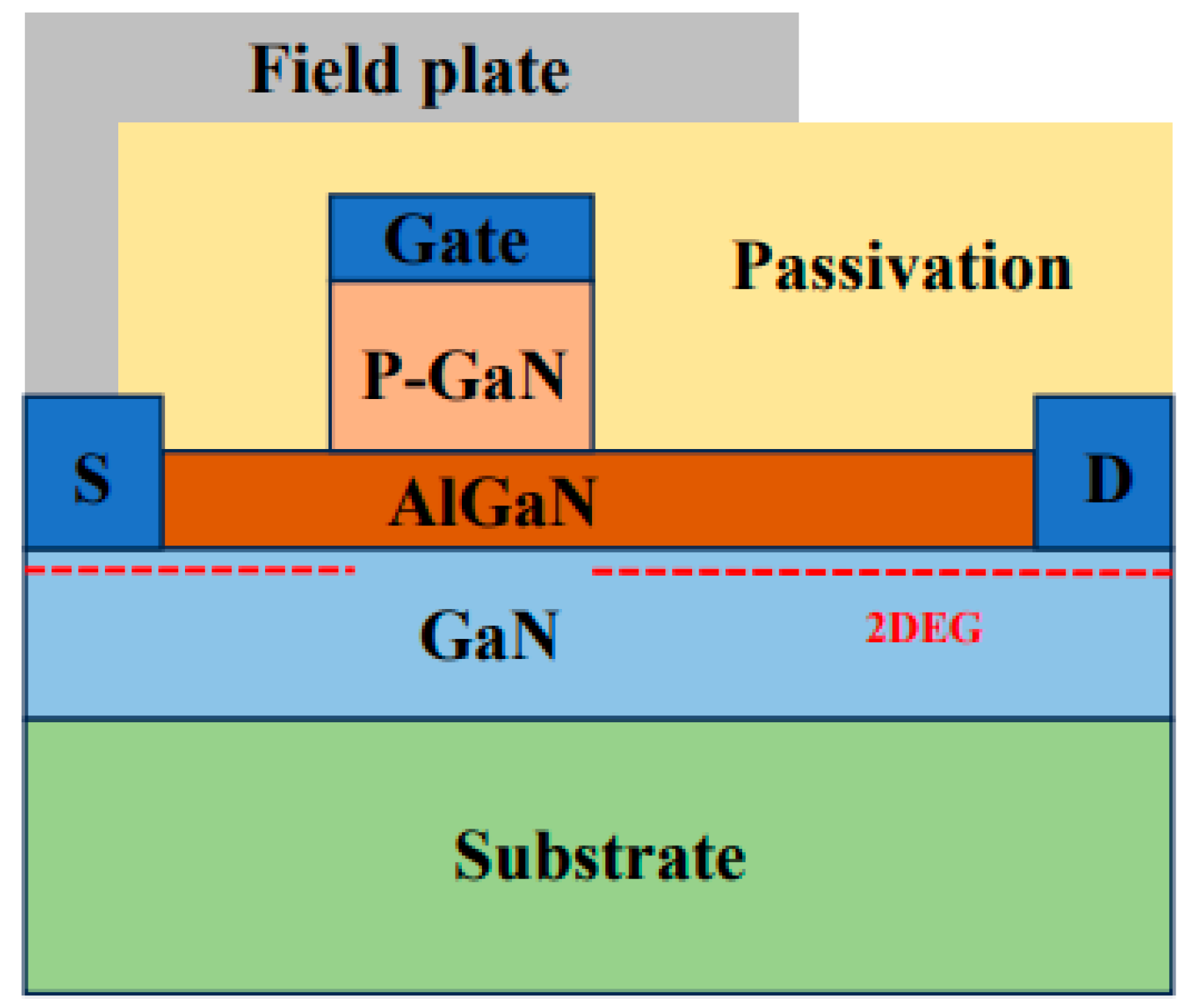
2. Materials and Methods

The devices tested in this work are commercially available 650 V E-mode AlGaN/GaN HEMTs with a Schottky p-GaN gate (GS-065-004-1-L-TR) [15]. Figure 1 illustrates the device schematic of p-GaN/AlGaN/GaN HEMT [16]. The measurement of I-V characteristics and the TDDB test were performed using Keithley’s 2410 and 2651A source meters coupled with a vacuum chamber and temperature controller. Figure 2a and Figure 2b show ID-VG and IG-VG curves of a p-GaN HEMT from −10 to 175 °C, respectively. The threshold voltage defined at ID = 1 mA with VD = 0.1 V was found to be 1.8 V at room temperature. For the TDDB experiment, a constant gate voltage was applied, and both the source and drain were set to ground. During the experiment, an abrupt increase in the gate stress current was identified as a failure at the gate stack of the device, and the test was repeated several times using identical devices with the same parameters.

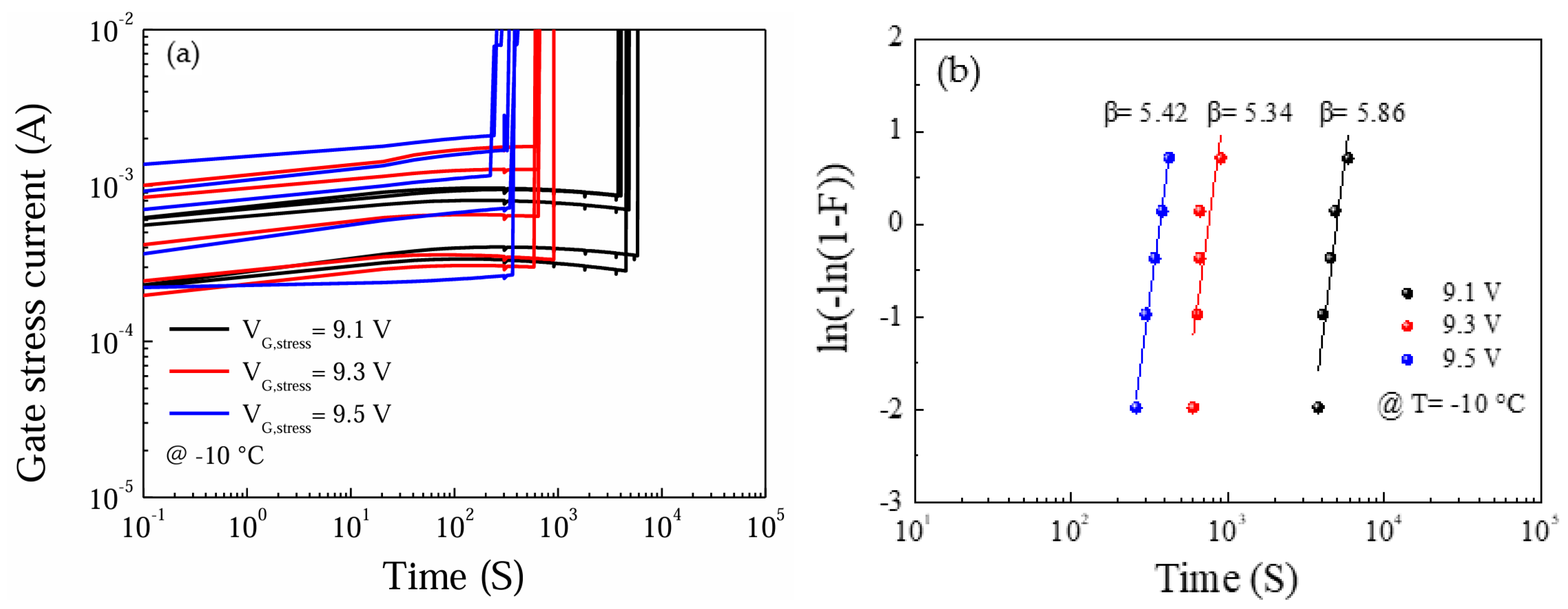
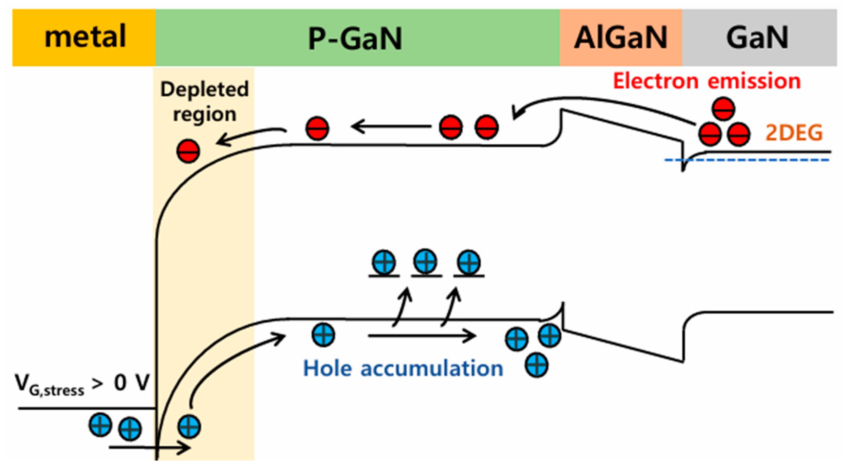
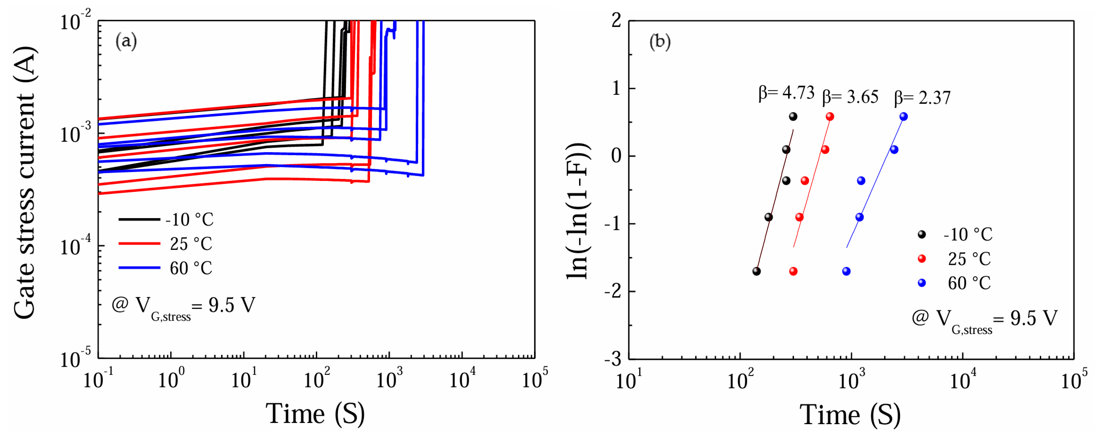
3. Results and Discussion

A constant gate voltage is applied during time-dependent gate breakdown measurements, with both the source and drain maintained at 0 V. Given that the gate-rated voltage of the device is 10 V, the gate stress voltage conditions were set to 9.1, 9.3, and 9.5 V. The time-to-breakdown (tBD) is identified as the critical point at which the gate stress current exhibits a sudden increase. The TBD results were analyzed to create a Weibull plot, which was then utilized to predict gate lifetime voltages at different temperatures.
Even under identical gate voltage conditions and for devices with the same structure, the time to breakdown (TBD) varies among devices. This probabilistic behavior is effectively modeled using the Weibull distribution [17]. The Weibull plot is based on the Weibull cumulative distribution function (CDF), which describes the probability of failure (F(t)) before a given time (t) as F(t) = 1 − exp(−(t/η)β). From the Weibull plot, both the scale factor (η) and shape factor (β) can be determined.
Figure 3a,b show the TBD measurement results at T of −10 °C and the corresponding Weibull plot derived from those results. The mean-time-to-failure (MTTF) corresponding to a 63% failure rate is 4973 s at 9.1 V, 755 s at 9.3 V, and 368 s at 9.5 V, showing a decrease as the stress voltage increases. Analysis based on Weibull distribution was proceeded in terms of the gate voltage other than the electric field because the electric field in the back-to-back gate diode of p-GaN/AlGaN/GaN structure is hardly straightforward compared with the oxide field of Si MOSFET.
Figure 4a shows the lifetime prediction at −10 °C, which is determined to be 7.45 V. This result is 0.7 V lower than the 10-year lifetime voltage at 60 °C, indicating that gate degradation in p-GaN HEMT becomes more severe at lower temperatures.
Figure 5 illustrates the schematic energy band diagram of the p-GaN gate HEMT under positive gate stress. In the Schottky-type p-GaN gate, applying a strong positive gate bias results in the injection of a considerable number of holes from the gate electrode into the p-GaN region. These holes either accumulate or become trapped at the p-GaN/AlGaN interface, effectively lowering the AlGaN energy barrier. Consequently, the electrons in the two-dimensional electron gas channel can overcome the lowered AlGaN barrier and move into the p-GaN region. As electrons reach the depletion of p-GaN, they interact with the holes present in the p-GaN layer. Under the influence of the strong electric field within the p-GaN layer, both carriers are energized as they accelerate significantly. The energized carriers induce impact ionization, leading to the formation of defects within the gate/p-GaN interface and the p-GaN layer, thereby causing degradation [18,19]. Under high-temperature stress, hole release from the p-GaN/AlGaN interface can be intensified. This results in a higher AlGaN energy barrier, effectively suppressing electron injection from the 2DEG into the p-GaN region. Consequently, the time-to-breakdown is extended at higher temperatures [20,21,22].
To analyze the temperature dependence of tBD, a gate stress voltage of 9.5 V was performed at various temperatures. Prior to the TDDB test, a gate step voltage stress experiment was conducted in the range of 0.5 V to 10 V with 0.5 V increments. Based on the experimental results, a gate breakdown voltage of 10 V was observed across all three temperatures, and the TDDB stress voltage was accordingly set to 9.5 V for each temperature condition. To examine TDDB characteristics under varying thermal conditions, experiments were conducted at −10, 25, and 60 °C with a step of 35 °C, and the experiments were repeated under the same gate stress for each temperature. The mean-time-to-failure (MTTF) corresponding to a 63% failure rate is 251 s at −10 °C, 501 s at 25 °C, and 1977 s at 60 °C, respectively, showing that low temperature accelerates the gate degradation in p-GaN HEMTs. As seen in Figure 6b, the shape factors(β) extracted from the Weibull plot are 4.73, 3.65, and 2.37 for −10, 25, and 60 °C, respectively, indicating that there is an increase in β with decreasing temperature. This suggests that the variation in time-to-breakdown (TBD) among devices becomes smaller at lower temperatures.
And as seen in Figure 7, the activation energy of −0.22 eV was extracted from the Arrhenius plot, which means that the degradation caused by forward gate voltage stress intensifies as the temperature decreases.

4. Conclusions

In conclusion, the gate degradation of p-GaN gate HEMTs under positive gate voltage has been analyzed at low temperatures. The 10-year rated voltage was determined from the Weibull plot, revealing that the value at −10 °C is lower than that at 60 °C. The activation energy of −0.22 eV was extracted from the Arrhenius plot, indicating that gate degradation in the p-Gan HEMTs is accelerated at low temperature. Under positive gate stress, degradation is caused by hole accumulation at the p-GaN/AlGaN interface, which facilitates electron injection from the 2DEG into the p-GaN region. The acceleration of these electrons by the gate electric field facilitates defect formation, ultimately causing breakdown. At high temperatures, the release of holes reduces the accumulation of positive charges, thereby extending the degradation time.

Author Contributions

Conceptualization, H.K. and J.Y.; methodology, J.Y.; validation, J.Y.; formal analysis, J.Y.; investigation, J.Y.; data curation, J.Y.; writing—original draft preparation, J.Y.; writing—review and editing, H.K.; visualization, J.Y.; supervision, H.K.; project administration, H.K.; funding acquisition, H.K. All authors have read and agreed to the published version of the manuscript.

Funding

This work was supported by NRF-2022M3I8A1077243 and National Research Foundation of Korea (NRF) grant funded by the Korea government (Ministry of Science and ICT) (RS-2024-00431359).

Data Availability Statement

The data presented in this study are available upon request from the corresponding author.

Conflicts of Interest

The authors declare no conflicts of interest.

References

  1. Ambacher, O.; Foutz, B.; Smart, J.; Shealy, J.R.; Weimann, N.G.; Chu, K.; Murphy, M.; Sierakowski, A.J.; Schaff, W.J.; Eastman, L.F.; et al. Two-dimensional electron gases induced by spontaneous and piezoelectric polarization in undoped and doped AlGaN/GaN heterostructures. J. Appl. Phys. 1999, 87, 334–344. [Google Scholar] [CrossRef]
  2. Ambacher, O.; Smart, J.; Shealy, J.R.; Weimann, N.G.; Chu, K.; Murphy, M.; Schaff, W.J.; Eastman, L.F.; Dimitrov, R.; Wittmer, L.; et al. Two-dimensional electron gases induced by spontaneous and piezoelectric polarization charges in N- and Ga-face AlGaN/GaN heterostructures. J. Appl. Phys. 1999, 85, 3222–3233. [Google Scholar] [CrossRef]
  3. Hassan, A.; Savaria, Y.; Sawan, M. GaN Integration Technology, an Ideal Candidate for High-Temperature Applications: A Review. IEEE Access 2018, 6, 78790–78802. [Google Scholar] [CrossRef]
  4. Haziq, M.; Falina, S.; Manaf, A.A.; Kawarada, H.; Syamsul, M. Challenges and opportunities for high-power and high-frequency AlGaN/GaN high-electron-mobility transistor (HEMT) applications: A review. Micromachines 2022, 13, 2133. [Google Scholar] [CrossRef] [PubMed]
  5. Greco, G.; Iucolano, F.; Roccaforte, F. Review of technology for normally-off HEMTs with p-GaN gate. Mater. Sci. Semicond. Proc. 2018, 78, 96–106. [Google Scholar] [CrossRef]
  6. Hilt, O.; Knauer, A.; Brunner, F.; Bahat-Treidel, E.; Wurfl, J. Normally-off AlGaN/GaN HFET with p-type GaN Gate and AlGaN Buffer. In Proceedings of the 2010 22nd International Symposium on Power Semiconductor Devices & IC’s (ISPSD), Hiroshima, Japan, 6–10 June 2010; pp. 347–350. [Google Scholar]
  7. Hwang, I.; Kim, J.; Choi, H.S.; Choi, H.; Lee, J.; Kim, K.Y.; Park, J.-B.; Lee, J.C.; Ha, J.; Oh, J.; et al. p-GaN Gate HEMTs With Tungsten Gate Metal for High Threshold Voltage and Low Gate Current. IEEE Electron Device Lett. 2013, 34, 202–204. [Google Scholar] [CrossRef]
  8. Zhou, G.; Zeng, F.; Jiang, Y.; Jiang, Q.W.L. Determination of the Gate Breakdown Mechanism in p-GaN Gate HEMTs by Multiple-Gate-Sweep Measurements. IEEE Electron Device Lett. 2021, 68, 1518–1523. [Google Scholar] [CrossRef]
  9. Meneghini, M.; Rossetto, I.; Rizzato, V.; Stoffels, S.; Van Hove, M.; Posthuma, N.; Wu, T.-L.; Marcon, D.; Decoutere, S.; Meneghesso, G.; et al. Gate Stability of GaN-Based HEMTs with P-Type Gate. Electronics 2016, 5, 14. [Google Scholar] [CrossRef]
  10. Wang, C.; Hua, M.; Yang, S.; Zhang, L.; Chen, K.J. E-mode p-n Junction/AlGaN/GaN HEMTs with Enhanced Gate Reliability. In Proceedings of the 2020 32nd International Symposium on Power Semiconductor Devices and ICs (ISPSD), Vienna, Austria, 13–18 September 2020; pp. 14–17. [Google Scholar] [CrossRef]
  11. Ťapajna, M.; Hilt, O.; Bahat-Treidel, E.; Würfl, J.; Kuzmík, J. Gate Reliability Investigation in Normally-Off p-Type-GaN Cap/AlGaN/GaN HEMTs Under Forward Bias Stress. IEEE Electron Device Lett. 2016, 37, 385–388. [Google Scholar] [CrossRef]
  12. Millesimo, M.; Fiegna, C.; Posthuma, N.; Borga, M.; Bakeroot, B.; Decoutere, S.; Tallarico, A.N. High-Temperature Time-Dependent Gate Breakdown of p-GaN HEMTs. IEEE Trans. Electron Devices 2021, 68, 5701–5706. [Google Scholar] [CrossRef]
  13. He, J.; Wei, J.; Yang, S.; Hua, M.; Zhong, K.; Chen, K.J. Temperature-Dependent Gate Degradation of p-GaN Gate HEMTs under Static and Dynamic Positive Gate Stress. In Proceedings of the 2019 31st International Symposium on Power Semiconductor Devices and ICs (ISPSD), Shanghai, China, 19–23 May 2019; pp. 295–298. [Google Scholar] [CrossRef]
  14. Rossetto, I.; Meneghini, M.; Hilt, O.; Bahat-Treidel, E.; De Santi, C.; Dalcanale, S.; Wuerfl, J.; Zanoni, E.; Meneghesso, G. Time-Dependent Failure of GaN-on-Si Power HEMTs With p-GaN Gate. IEEE Trans. Electron Devices 2016, 63, 2334–2339. [Google Scholar] [CrossRef]
  15. GS-065-004-1-L. Datasheet. GaN Systems. 2022. Available online: http://www.gansystems.com (accessed on 1 August 2024).
  16. Chae, M.; Kim, H. Investigation of the Gate Degradation Induced by Forward Gate Voltage Stress in p-GaN Gate High Electron Mobility Transistors. Micromachines 2023, 14, 977. [Google Scholar] [CrossRef] [PubMed]
  17. Bhattacharya, P.; Bhattacharjee, R. A study on Weibull distribution for estimating the parameters. Wind Eng. 2009, 33, 469–476. [Google Scholar] [CrossRef]
  18. Wu, T.-L.; Marcon, D.; You, S.; Posthuma, N.; Bakeroot, B.; Stoffels, S.; Van Hove, M.; Groeseneken, G.; Decoutere, S. Forward Bias Gate Breakdown Mechanism in Enhancement-Mode p-GaN Gate AlGaN/GaN High-Electron Mobility Transistors. IEEE Electron Device Lett. 2015, 36, 1001–1003. [Google Scholar] [CrossRef]
  19. Tallarico, A.N.; Stoffels, S.; Magnone, P.; Posthuma, N.; Sangiorgi, E.; Decoutere, S.; Fiegna, C. Investigation of the p-GaN Gate Breakdown in Forward-Biased GaN-Based Power HEMTs. IEEE Electron Device Lett. 2017, 38, 99–102. [Google Scholar] [CrossRef]
  20. Masin, F.; Meneghini, M.; Canato, E.; De Santi, C.; Stockman, A.; Zanoni, E.; Moens, P.; Meneghesso, G. Positive temperature dependence of time-dependent breakdown of GaN-on-Si E-mode HEMTs under positive gate stress. Appl. Phys. Lett. 2019, 115, 052103. [Google Scholar] [CrossRef]
  21. He, J.; Wei, J.; Li, Y.; Zheng, Z.; Yang, S.; Huang, B.; Chen, K.J. Characterization and analysis of low-temperature time-to-failure behavior in forward-biased Schottky-type p-GaN gate HEMTs. Appl. Phys. Lett. 2020, 116, 223502. [Google Scholar] [CrossRef]
  22. He, J.; Wei, J.; Zheng, Z.; Yang, S.; Li, Y.; Huang, B.; Chen, K.J. Low-Temperature Accelerated Gate Reliability of Schottky-type p-GaN Gate HEMTs. In Proceedings of the 2020 32nd International Symposium on Power Semiconductor Devices and ICs (ISPSD), Vienna, Austria, 13–18 September 2020; pp. 290–293. [Google Scholar] [CrossRef]
Figure 1. Device schematic of p-GaN gate AlGaN/GaN HEMT.
Electronics 14 01764 g001
Figure 2. (a) ID-VG curves and (b) IG-VG curves of p-GaN gate HEMT at various temperatures.
Electronics 14 01764 g002
Figure 3. (a) tBD characteristics at gate stress of 9.1 V, 9.3 V, 9.5 V (b) Weibull plot of tBD distribution at T of −10 °C.
Electronics 14 01764 g003
Figure 4. Extrapolation of maximum forward Vg for period of 10-years at (a) −10 °C and (b) 60 °C.
Electronics 14 01764 g004
Figure 5. Schematic energy band diagrams of Schottky p-GaN gate HEMTs with an applied positive gate bias.
Electronics 14 01764 g005
Figure 6. (a) TBD characteristics at different temperatures of −10, 25, 60 °C (b) Weibull plot of tBD distribution at VG,stress = 9.5 V.
Electronics 14 01764 g006
Figure 7. Arrhenius plot of VG,stress = 9.5 V.
Electronics 14 01764 g007
Disclaimer/Publisher’s Note: The statements, opinions and data contained in all publications are solely those of the individual author(s) and contributor(s) and not of MDPI and/or the editor(s). MDPI and/or the editor(s) disclaim responsibility for any injury to people or property resulting from any ideas, methods, instructions or products referred to in the content.

