1. Introduction
Content-Addressable Memories (CAMs) are critical components in high-performance computing and data analysis. They enable fast data lookup operations, which are essential for many applications. For example, CAMs are used in packet routing and switching [
1,
2]. They also play a role in DNA sequence analysis [
3,
4]. In addition, CAMs support machine learning and data analysis, especially with approximate CAM designs [
5].
Unlike traditional Random-Access Memories (RAMs), which access data using specific addresses, CAMs enable parallel content search. This significantly speeds up lookup operations and is especially crucial in data plane packet processing. Tasks like IP address lookup, access control, and flow classification demand fast and efficient search mechanisms to meet strict throughput and latency requirements [
6].
Various CAM types serve distinct roles within packet processing pipelines. Binary CAMs (BCAMs) are optimized for exact match lookups, making them ideal for applications such as MAC address tables, as illustrated in
Figure 1. Ternary CAMs (TCAMs) support wildcard-based matching, allowing flexible rule definitions that are indispensable in applications such as access control lists (ACLs) and packet classification. Additionally, a specific type of TCAM could only consider prefix matching to handle Longest Prefix Match (LPM) operations, which are crucial in IP routing. In LPM, each subnet in a network defines a range of IP addresses with a common prefix, and STCAMs efficiently match these prefixes to determine the most specific routing entry for a given IP address. This specialized functionality makes STCAMs highly effective in network IP matching and routing table lookups, where hierarchical addressing schemes are prevalent.
Despite their advantages, implementing CAMs for high-throughput environments presents several challenges. Traditional CAM designs, often realized through Application-Specific Integrated Circuits (ASICs), offer excellent performance but suffer from high development costs and lack flexibility for evolving network requirements. The adoption of Field-Programmable Gate Arrays (FPGAs) for CAM implementations has surged due to their inherent parallel processing capabilities and reconfigurability, offering flexibility over traditional Application-Specific Integrated Circuits (ASICs). FPGA-based CAMs are typically realized using four primary on-chip memory types: Ultra RAM (URAM), Block RAM (BRAM), Lookup Table RAM (LUTRAM), and flip-flops (FFs). Each memory type presents trade-offs in terms of resource utilization, power efficiency, and scalability. For example, BRAM-based CAMs offer high density but suffer from longer update latencies, whereas LUTRAM-based CAMs provide faster updates at the cost of increased routing complexity. FF-based CAMs, though less scalable, excel in applications requiring minimal hardware overhead and rapid updates.
FPGAs offer a reconfigurable alternative that can provide CAM performance while providing additional adaptability. However, traditional Register-Transfer Level (RTL) design methods for implementing CAMs on FPGAs present several challenges. These approaches are complex, time-consuming, and error-prone, which hinders rapid prototyping and design space exploration. High-Level Synthesis (HLS) addresses these limitations by introducing a new design paradigm. HLS allows hardware description using high-level programming languages like C/C++, significantly simplifying the development process.
HLS also facilitates accelerated development cycles, improved design portability, and simplified integration with software-driven workflows. While HLS has demonstrated its potential in various application domains, to the best of our knowledge, no prior work specifically addresses the design and implementation of CAM architectures optimized for packet processing using HLS.
This gap in the literature motivates the present paper, which proposes HLSCAM (
https://github.com/abbasmollaei/HLSCAM, accessed on 24 April 2025) an HLS-based approach to implement CAM architectures optimized for data plane packet processing on FPGAs. The contributions of the paper include the following:
It presents a templated HLS-based implementation of BCAMs for exact matching and TCAMs for ternary matching, supporting arbitrary table sizes for data plane packet processing.
It explores the trade-offs between resource and latency to flexibly cover the design space for different FPGA-based packet processing use cases.
It leverages FPGA parallelism through applying varied design parameters and optimization directives for CAM implementation in HLS to achieve high operating frequencies with minimal latency.
It explores the design space for CAMs by varying memory depths, key widths, and optimization methods applied to evaluate performance and resource occupation comprehensively.
The remainder of this paper is structured as follows.
Section 2 reviews related work on FPGA-based CAM implementations.
Section 3 presents the proposed HLS-based CAM design, detailing the architectural framework, optimization strategies for BCAM, TCAM, and memory allocation schemes.
Section 4 describes the experimental environment and provides a comprehensive analysis of the results, including design space exploration, performance evaluation based on various metrics, and a comparison with State-of-the-Art approaches. Finally,
Section 5 concludes the paper by summarizing key findings and highlighting potential directions for future research.
2. Literature Review
Extensive research has been conducted to optimize FPGA-based CAM architectures, focusing on improving throughput, reducing power consumption, and enhancing resource efficiency. Early implementations, such as the Hybrid Partitioned TCAM (HP-TCAM) [
7], introduced partitioning techniques to mitigate the exponential growth in resource requirements associated with brute-force approaches. Although HP-TCAM improved memory efficiency, it required pre-processed, ordered data and lacked dynamic update capabilities. Subsequent designs, such as Ultra-Efficient TCAM (UE-TCAM) [
8], further optimized resource utilization by reducing redundant memory structures, even though these designs remained reliant on complex Register-Transfer Level (RTL) methodologies. An FPGA-based method for the construction of deep and narrow BCAMs using Segmented Transposed Indicators RAM (STIRAM) is proposed in [
9]. This approach stores segment indicators and patterns in separate RAM structures, enabling a two-cycle match operation with concurrent reading. The authors in [
10] introduce FMU-BiCAM algorithms for binary CAMs on FPGA, achieving two-cycle updates by directly using CAM keys as addresses. It reduces power consumption by eliminating lookup tables and limiting updates to necessary SRAM blocks.
LUTRAM-based CAM architectures, such as DURE-TCAM [
11], D-TCAM [
12], and ME-TCAM [
13], have demonstrated improved update efficiency and reduced latency. DURE-TCAM [
11] introduced a dynamically updateable TCAM architecture for FPGAs that uses LUTRAM primitives. DURE addresses the issue of blocking updates in existing SRAM-based TCAMs by enabling simultaneous search and update operations. The D-TCAM architecture [
12] uses 6-input LUTRAMs to emulate 6-bit TCAM, and combines 64 of these LUTRAMs to create a 48-byte D-CAM block. These D-CAM blocks are cascaded horizontally and vertically to increase the width and depth of the TCAM, respectively. It also exploits the LUT-FF pair nature of FPGAs, using redundant flip-flops as pipeline registers.
ME-TCAM [
13] introduces a Memory-Efficient Ternary Content Addressable Memory scheme using multipumping-enabled LUTRAM on FPGAs to enhance memory efficiency over traditional SRAM-based TCAMs. The TCAM table is partitioned into Hybrid Partitions (HPs), with each HP simulated using four LUTRAMs. However, increasing the multipumping factor improves memory efficiency at the cost of reduced throughput. RPE-TCAM [
14] proposes a reconfigurable power-efficient TCAM for FPGAs that reduces power consumption by 40% using selective bank activation. It maintains one-cycle update latency and supports BiCAM and TCAM configurations. A backup CAM (BUC) handles bank overflow, ensuring efficient memory use.
An SRAM-based TCAM architecture (REST) is proposed in [
15]. It improves memory efficiency by optimizing address mapping using virtual blocks (VBs). By dividing SRAM into multiple VBs, REST increases the emulated TCAM capacity while reducing throughput. The design allows a trade-off between memory efficiency and throughput by adjusting the number of VBs. A multi-region SRAM-based TCAM architecture for longest prefix matching is presented in [
16], reducing memory area usage by dividing TCAM entries into index and data fields. The index maps to SRAM addresses, while the data stores content, improving memory efficiency. Another work [
17] presents power-efficient FPGA-based TCAM architecture using a segmented match line strategy to reduce dynamic power consumption. Each match line is divided into four nine-bit segments, activated sequentially to prevent unnecessary power usage.
Meanwhile, flip-flop-based designs like LH-CAM [
18] and G-AETCAM [
19] explored the use of FPGA slice registers to achieve low-latency, high-speed CAM operations. While these designs achieved impressive performance for small-scale implementations, they faced scalability challenges due to routing complexity and hardware overhead.
TeRa [
2] introduces a ternary and range-based CAM architecture for packet classification, offering a power-efficient alternative to TCAMs. It features Ternary Match Logic (TML) with NAND-NOR encoding, a carry tree-based Range Match Logic (CTRC) for range comparisons, and Match Inversion Logic for efficient rule handling. TYPE1 is optimized for ASICs, while TYPE2 is adaptable for both ASICs and FPGAs, enhancing priority selection and memory efficiency.
A reconfigurable match table (RMT) design for FPGA-based switches has been proposed in [
1], incorporating a TCAM-based implementation for flexible packet processing. The design employs a three-layer structure enabling dynamic reconfiguration of match table size and type without hardware modification. A segment crossbar facilitates PMT sharing and signal conversion, including a MAND operation for combining match lines across TCAM PMTs.
Despite these advances, existing research predominantly focuses on RTL-based design methodologies. While RTL offers fine-grained control over hardware resources, it is inherently time-consuming, complex, and less adaptable to evolving design requirements. HLS offers more flexibility, enables faster development, enhances design portability, and simplifies design space exploration. While CAM architectures have been extensively explored at the RTL and lower design levels, HLS-based implementations remain largely unexplored, particularly for designing match-action tables in packet processing applications.
3. Potential Network Applications
The proposed HLS-based CAM architecture is particularly suited for high-speed data plane operations in modern networking systems. Its flexibility and configurability enable efficient integration into various packet processing applications. Below are several use cases that illustrate how CAMs can be practically deployed in real-world networking environments.
3.1. Packet Classification and Filtering
CAMs are commonly used to match packet header fields (e.g., IP addresses, protocol numbers, port numbers) against a set of predefined rules. This operation is fundamental in routers, firewalls, and switches to determine the appropriate action for each packet, such as forwarding, dropping, or rate-limiting. For example, a TCAM can match the quintuple of an incoming packet (source/destination IP and port, and protocol) with a set of entries in the Access Control List (ACL), allowing multi-field classification in a single clock cycle [
20].
3.2. Firewall and Intrusion Detection Systems (IDS)
TCAMs are ideal for rule-based packet inspection, where wildcard matching is often required. For example, a firewall can use TCAM entries to define rules such as ‘allow all traffic from subnet 192.168.0.X’, using ternary bits to represent masked fields. IDS applications benefit similarly by matching known attack signatures or suspicious traffic behavior patterns across various protocol headers, providing real-time threat detection [
21].
3.3. In-Band Network Telemetry (INT)
CAMs can be used to identify specific flows that require telemetry information insertion. Upon a CAM match, INT metadata is appended to the packet to track path information (e.g., latency, hop count) through the network. This enables operators to monitor network performance and detect anomalies with minimal overhead [
22].
3.4. Network Address Translation (NAT)
In NAT-enabled devices, CAMs can serve as lookup tables to translate between internal private IP addresses and external public addresses. By maintaining a CAM of current translation entries, the device can efficiently identify and rewrite packet headers during ingress and egress processing [
23].
3.5. Time-Sensitive Networking (TSN)
In deterministic networking environments, such as industrial automation or autonomous systems, CAMs help enforce strict scheduling and traffic-shaping rules. By matching packets against timing-based policies, CAMs enable precise control of transmission schedules to meet latency and reliability requirements [
24].
3.6. User Management in 5G Core
CAMs play a crucial role in user session management and packet forwarding in 5G core network components, such as the User Plane Function (UPF) [
25] and Access Gateway Function (AGF) [
26]. In these 5G core sections, CAMs are used to match packet headers against subscriber session entries to enforce policy rules, quality-of-service (QoS) settings, and forwarding paths. This enables real-time user plane operations, including traffic steering, usage reporting, and IP anchor point management, all of which demand low-latency, high-throughput processing.
4. CAM Architectures, Implementations, and Trade-Offs
This work presents a templated HLS-based design and implementation of BCAM and TCAM architectures, adjusted for data plane packet processing applications on FPGAs. Our approach leverages the Vitis HLS tool for AMD (Xilinx) FPGAs, focusing on three distinct design perspectives: Brute Force (BF), Balanced (BL), and High-Speed (HS). Each perspective addresses specific trade-offs between resource utilization, latency, and throughput, achieved by fine-tuning hardware directives provided by the Vitis HLS tool. Various design directives are applied to configure memory space allocation and access patterns based on application requirements to manage FPGA parallelism precisely. Additionally, the implementation is structured to allow the synthesis tool to optimize timing constraints and reach high operating frequencies.
4.1. Design Perspectives
4.1.1. Brute-Force CAM
The Brute-Force method implements sequential memory access, processing lookups two entries at a time.
Figure 2 illustrates the hardware structure of the proposed CAM lookup in BF mode. The search engine is responsible for sequentially reading each entry and executing the required comparison and matching operations, depending on the CAM type. The allocated memory space consists of a single memory module with two ports for the entire CAM table. The first port is dedicated to read-only operations, while the second port supports both read and write functions.
This approach prioritizes minimal resource utilization, making it ideal for applications with strict hardware limitations. Although it greatly reduces the consumption of FPGA resources, it introduces higher latency because of the restricted number of memory ports and the resulting serialized search procedure.
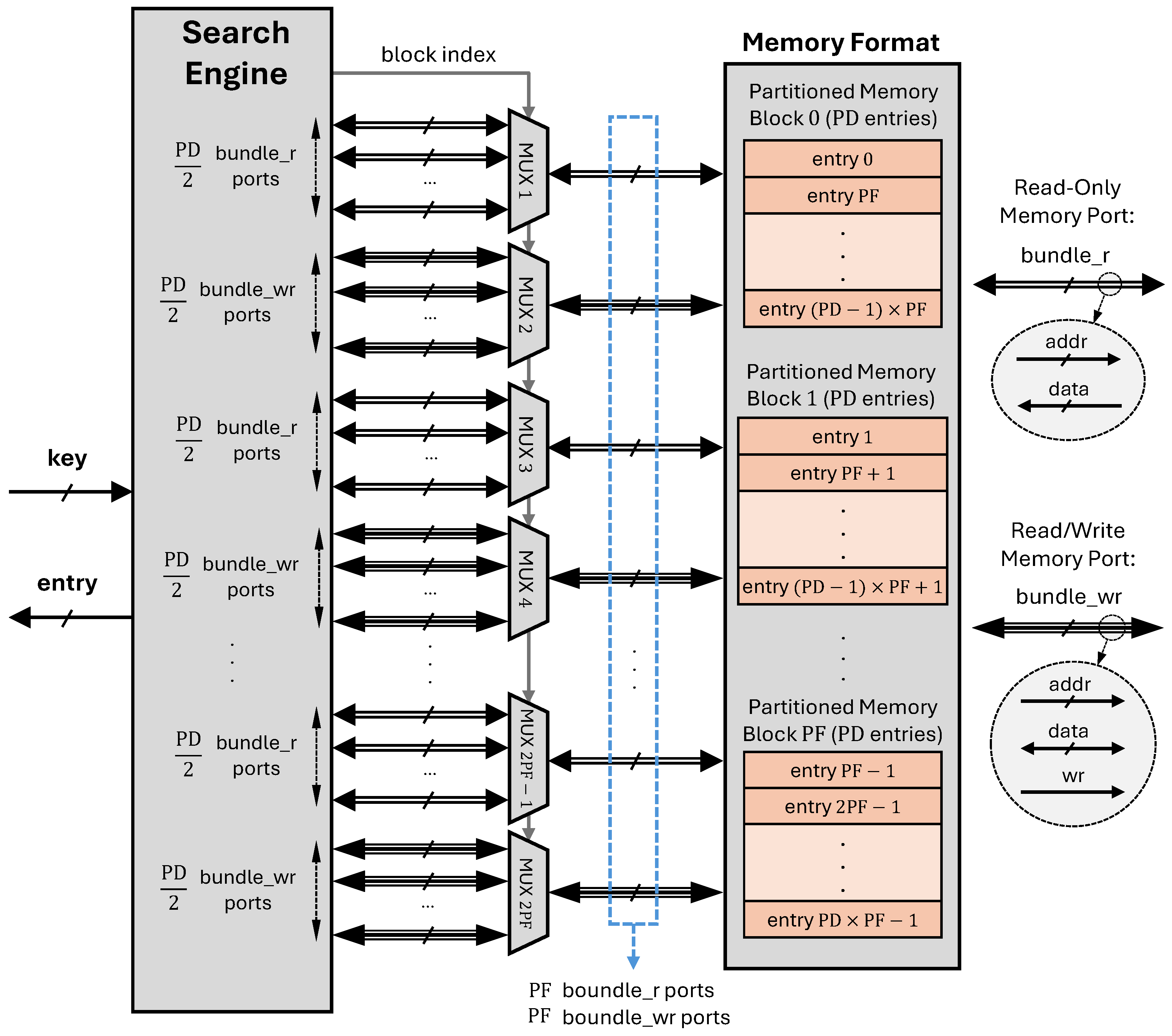
4.1.2. Balanced CAM
The Balanced method aims to provide a trade-off between resource utilization and performance. This architecture employs partial parallelism in memory access, where search operations are distributed across multiple parallel memory units.
Figure 3 depicts the proposed CAM lookup hardware structure in BL mode. Consequently, the memory is divided into
(Partition Factor) blocks, each containing
(Partition Depth) entries. The relationship between
and
is defined by Equation (
1).
This partitioning scheme increases the number of memory ports by a factor of
, resulting in 2 ×
ports. Consequently, the search engine requires
clock cycles to read all entries. Thus, the minimum achievable latency in the BL method is
cycles, excluding the additional processing time required to identify the correct matching entry. During operation, the search engine schedules entry addresses and selects the appropriate address at each clock cycle using multiplexers, retrieving the entries for the matching process. The memory port signals are organized into two bundles:
bundle_r for read-only ports and
bundle_wr for read/write ports.
This approach reduces latency compared to the BF method while maintaining moderate resource usage. In Vitis HLS, we achieved this balance by selectively applying partial memory block partitioning, loop unrolling, and pipelining directives, allowing controlled parallel data paths. This design is well-suited for scenarios where both performance and resource efficiency are critical, such as mid-range packet processing applications.
4.1.3. High-Speed CAM
The High-Speed method is optimized for maximum throughput and minimal latency, fully exploiting the parallelism of FPGAs to enable simultaneous comparisons across multiple CAM entries. As illustrated in
Figure 4, the hardware architecture in High-Speed mode features a flattened memory structure, where each entry is assigned a dedicated memory port. This configuration allows the search engine to access all entries within a single clock cycle, achieving the lowest possible latency compared to other modes. We extensively utilized directives such as full loop unrolling, aggressive pipelining, and array partitioning in Vitis HLS to maximize data flow concurrency. While this approach results in higher resource utilization, it achieves the lowest possible latency.
Given the parallel nature of operations in the HS mode, the intermediate wiring and routing logic consume significant FPGA resources. We introduce an enhanced version of the HS mode, referred to as HS-H, to improve resource efficiency. The HS-H architecture follows a hierarchical design. It matches the input key and returns the index of each matching entry, or an invalid value if no match is found. The valid indexes are then forwarded through tree-based multiplexers. This hierarchical approach reduces the number of intermediate signals propagating across multi-cycle matching operations, thereby saving logic resources compared to the original HS mode. However, the trade-off shows a slight increase in the required number of clock cycles due to the added hierarchical structure.
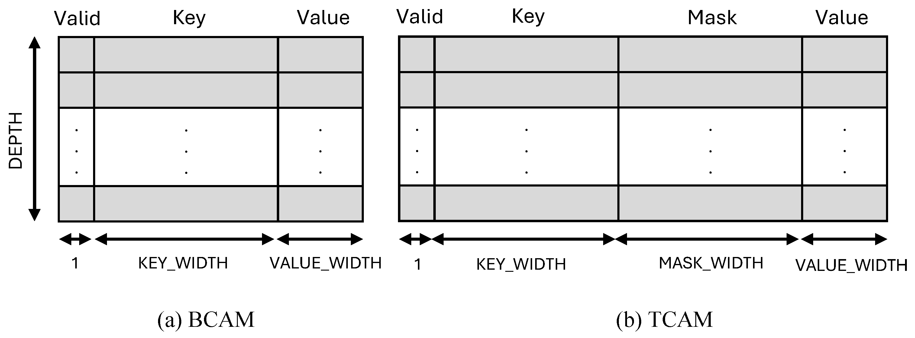
4.2. BCAM
The BCAM implementation follows a template-based structure, allowing for the flexible parameterization of key width, value width, and depth. The core structure of BCAM consists of an array of entries, where each entry is defined by a key, a corresponding value, and a validity flag as shown in
Figure 5a. The BCAM is implemented as a class template (BCAM<KEY_WIDTH, VALUE_WIDTH, DEPTH>) to support a customizable key size, value size, and memory depth.
The search_entry function performs an exact match lookup by iterating through all entries, with its level of parallelism determined by the selected optimization mode. In HS mode, full parallelism is applied by distributing over distinct memory blocks, allowing all entries to be checked simultaneously for minimal latency. In BL mode, the degree of parallelism is proportionally determined by the , as higher values enable more memory partitions to be accessed concurrently, enhancing parallel lookup. In BF mode, the search is fully sequential, processing one entry at a time without parallelism. The function finally finds the matched index and returns the corresponding entry.
4.3. TCAM
Ternary matching in TCAM allows each bit of a stored key to represent ‘0’, ‘1’, or a wildcard (‘X’). This is implemented by associating each key bit with a corresponding mask bit. When a mask bit is enabled, the associated key bit becomes a wildcard, matching both ‘0’ and ‘1’ during lookup. For example, a stored IPv4 prefix of 192.168.1.X (C0.A8.01.XX) can be represented by a key and a mask where the last six bits are masked, allowing any value in those positions. This would match IP addresses such as 192.168.1.10 (C0.A8.01.0A) or 192.168.1.63 (C0.A8.01.3F).
The proposed TCAM class provides a templated key-value storage system that supports ternary matching, allowing wildcard bits in key comparisons. Each entry consists of a key, a mask, a value, and a validity flag, as shown in
Figure 5b. The
search_entry function performs a lookup by iterating over all entries and checking for a ternary match. As illustrated in
Figure 6, the matching process occurs in two stages. In the first stage, the function applies a bitwise XNOR between the stored and input keys to determine bit similarity. The result is then masked using the stored mask, and a validity check is performed. The outcome is stored as a Boolean value in an array, indicating whether each entry is a potential match. In the second stage, the Parallel Valid Index Finder (PVIF) module scans the array to locate the first valid match and retrieves the corresponding index and entry.
4.4. Memory Allocation
The proposed HLSCAM solution employs different memory allocation strategies in BF, BL, and HS modes, optimizing the use of FPGA resources based on performance and parallelism requirements. The primary memory resource utilized in the BF and the BL modes is LUTRAM, while the HS mode relies on register-based storage to maximize parallel access.
In the HS mode, the CAM array is fully flattened and mapped into FPGA registers, enabling simultaneous access to all entries. This approach eliminates the sequential memory access bottleneck associated with LUTRAM, allowing each lookup to be processed in a single cycle. However, storing CAM entries in registers instead of LUTRAM significantly increases FF utilization, which may become a limiting factor in large-scale CAM deployments. Each bit of a CAM entry in HS mode is mapped to a dedicated FF, allowing true parallel access and one-cycle lookup latency. This direct mapping ensures that all entries are immediately accessible without sequential memory traversal. However, such register-based implementation requires individual addressing for each bit, which can introduce additional logic overhead for managing lookup control and can complicate placement and routing during synthesis. This trade-off between speed and resource consumption must be carefully balanced, particularly for large-scale CAMs.
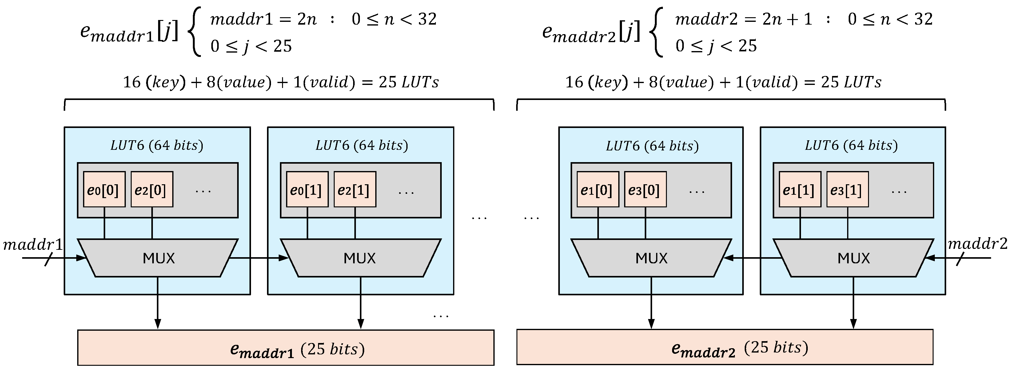
In the BF and BL modes, the CAM architecture utilizes LUT6 (LUT 6-input) elements configured as LUTRAM, where each LUT6 can store 64 bits.
Figure 7 illustrates the LUT6 organization for a BCAM depth of 64 entries, each with a 25-bit width (1-bit valid flag, 16-bit key, and 8-bit value) in the BF mode. To accommodate the dual-port memory access used in BF mode, the entries are divided into two groups:
Each group contains 32 entries, and all LUTs within a group share the same address input to provide simultaneous access. Each bit of an entry is stored at the same LUT address across different LUTs. Given the 25-bit entry width, 25 LUTs are required per group, resulting in a total of 50 LUTs for this BCAM configuration. However, due to the fixed 64-bit capacity per LUT, half of the bits in each LUT remain unused, leading to lower LUTRAM utilization efficiency. If the CAM architecture were configured with a single memory port instead of two, the LUT usage would be reduced by half, requiring only 25 LUTs instead of 50. However, this would come at the cost of approximately doubling the lookup latency, as each cycle could only access one entry at a time instead of two.
In this mode, the HLSCAM employs two memory ports to divide entries into two groups: even indexes and odd indexes. The even entries are mapped at the left group of LUTs, and the odd entries are mapped in the right group of LUTs, placing 32 entries into each group. The address input for the LUTs of each group is the same. Each bit of entries is distributed to the same address at LUTs. Since the entry width is 25 bits, 25 LUTs are needed for each group, occupying 50 LUTs in total. In this case, half the bits of each LUT remains unused. If we had single memory ports, the LUT usage would be half, and the latency would be around doubled.
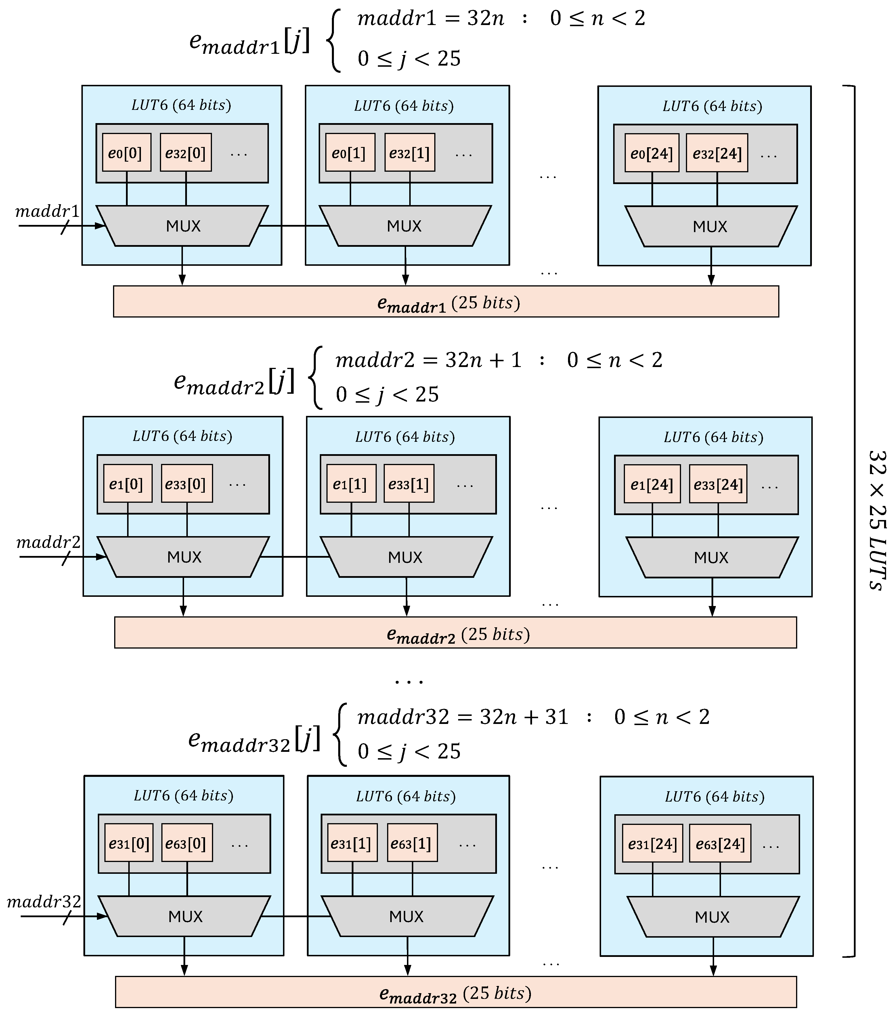
Although double-port memory used in the BF mode provides an efficient memory structure, it suffers from limiting the available memory bandwidth, resulting in linearly growing latency by increasing the CAM depth. The CAM storage is partitioned across more than two LUTs to enable parallel memory access, a process controlled by the
parameter. The
determines the number of LUTs allocated per CAM configuration, directly influencing memory access parallelism and resource utilization.
Figure 8 shows a
Higher values allocate more LUTs to store CAM entries, increasing parallel read/write access and reducing lookup latency. However, higher values also lead to LUTRAM fragmentation, as each partitioned LUT may contain unused bits that cannot be reassigned to other memory segments. This results in lower LUTRAM utilization efficiency despite improved parallelism.
In the BF mode, sequential lookups require minimal partitioning, leading to higher LUT utilization efficiency but increased lookup latency due to serial memory access. In contrast, the BL mode introduces a moderate level of partitioning, striking a balance between parallel memory access and LUTRAM efficiency.
5. Evaluation
This section evaluates the HLS-based BCAM and TCAM implementations under various design spaces. The evaluation focuses on measuring latency, maximum frequency, throughput, and FPGA resource utilization, highlighting the trade-offs between performance and hardware efficiency. Latency was measured in terms of the number of clock cycles required for a single lookup operation. At the same time, throughput was computed based on the operating frequency and parallelism in memory access.
5.1. Experimental Setup
The BCAM and TCAM architectures were implemented using AMD Vitis HLS 2023.2, which enables high-level hardware description and optimization for FPGAs. The synthesized designs were evaluated using AMD Vivado to collect detailed resource utilization reports. The AMD Alveo U280 FPGA (xcu280-fsvh2892-2L-e) was targeted as a high-performance acceleration card well-suited for high-throughput networking applications. The initial clock frequency was set to 312.5 MHz to align with standard high-speed networking requirements, such as those in 10G and 25G Ethernet systems. The maximum operating frequency () was determined based on the critical path identified during FPGA synthesis and post-place-and-route analysis. All reported results were obtained after placement and routing to ensure accurate performance evaluation.
5.2. Design Space Exploration
The design space of the proposed CAM architectures was explored by varying CAM depth, key width, and optimization methods. The evaluation considered three different table depths: 64, 128, and 256 entries. The 32, 64, and 128 key widths were chosen to analyze the impact of various configurations on performance and resource utilization. The stored value word width remained constant, as the complexity of the matching process depends mostly on the key rather than the stored value. Moreover, the
was fixed to 16 to divide CAMs into 16 partitions and provide 32 distinct memory ports. These variable parameters were selected to restrict the design space for focused analysis. At the same time, the proposed templated HLSCAM can go beyond these parameters that we evaluate with higher parameters in the
Section 5.5. This exploration allowed us to identify optimal configurations that balance efficiency, scalability, and application-specific requirements.
The synthesis performance and utilization of resources of the proposed BCAM architecture was evaluated in different configurations, as presented in
Table 1. In the BF mode, both LUT and register usage increase proportionally with growing table depth and key width. Latency directly correlates with CAM depth, as each lookup requires sequential comparisons. The measured latencies are 33, 65, and 129 clock cycles for 64, 128, and 256 entries, respectively. The maximum operating frequency varies between 346 MHz and 397 MHz, depending on key width and resource constraints.
In the BL mode, LUT Logic and LUTRAM usages grow linearly with key width but LUTRAM usage remains constant as the BCAM depth increases. This behavior results from
being fixed at 16 across all depths. As described by Equation (
2), the number of required LUTRAMs remains unchanged until the partitioned memory blocks can no longer accommodate additional bits, increasing LUTRAM usage. Register utilization follows a similar trend, changing slightly with depth variations but linearly increasing with key width. Depending on key width and depth, the maximum lookup latency varies from 4 to 10 clock cycles. The maximum operating frequency is variable from 306 MHz to 349 MHz, which is relatively lower than that of the BF mode.
In the HS mode, the tool shifts from LUTRAM storage to register-based storage for fully partitioned entries, reducing total LUT utilization. While LUT usage in HS mode is lower than in BL mode for depths of 64 and 128 entries, it increases significantly for 256-entry configurations due to the higher intermediate logic and wiring requirements for parallel processing. The use of registers grows more rapidly than in the BL mode, reflecting the use of registers to store BCAM entries. The lookup latency is minimized to one cycle for 64 entries with a key width of 32, while it increases to two cycles for larger configurations. The maximum operating frequency ranges from 314 MHz to 345 MHz, which are close to the BL mode.
The TCAM architecture exhibits synthesis performance trends similar to BCAM as presented in
Table 2, with increased resource utilization due to the added complexity of ternary matching and additional storage required for mask bits. Compared to BCAM, LUT, and register usage are approximately doubled across all configurations. Latency remains identical to BCAM, maintaining 33, 65, and 129 cycles in the BF mode and ranging between 5 and 10 cycles in the BL mode. In the HS mode, lookup latency remains at one or two cycles, depending on the key width and table depth. The range of maximum operating frequencies is slightly wider than in BCAM, varying from 294 MHz to 412 MHz.
5.3. BCAM Versus TCAM
This subsection compares the proposed BCAM and TCAM across different optimization modes, focusing on FPGA resource utilization and maximum clock frequency. The comparison is based on BCAM and TCAM architectures with depths of 128 and 256, while keeping the key width fixed at 128-bit and the value width at 8-bit.
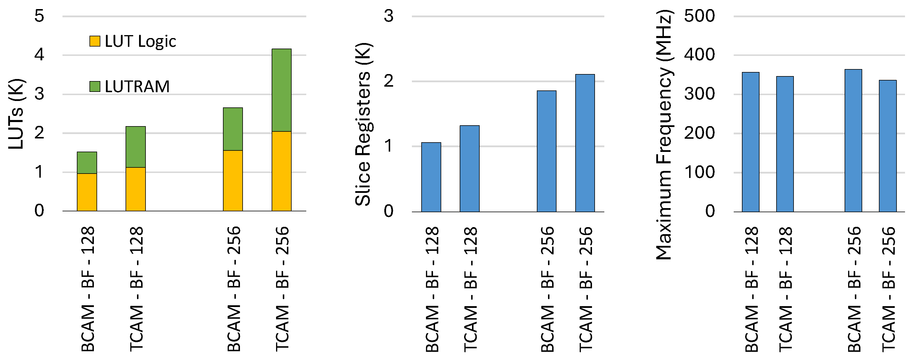
Figure 9 compares BCAMs and TCAMs in BF mode in terms of LUT and slice register consumptions, as well as frequency. The LUT consumption is a combination of LUT logic and LUTRAMs, which are shown in the chart separately. As expected, LUTRAM usage in TCAM is approximately twice that of BCAM, reflecting the increased memory demand for storing mask bits. In contrast, LUT logic usage is nearly identical for both architectures, with only minor differences, since both require the same logic for sequential memory iteration and matching operations. Accordingly, TCAM consumes more total LUTs than BCAM. TCAM also requires 24% more registers for 128-depth configurations and 14% more for 256-depth configurations than BCAM. Moreover, BCAM achieves slightly higher maximum operating frequencies, surpassing TCAM by approximately 3% in the 128-depth case and 8% in the 256-depth case.
In the BL mode, the resource utilization gap between BCAM and TCAM becomes more pronounced, as shown in
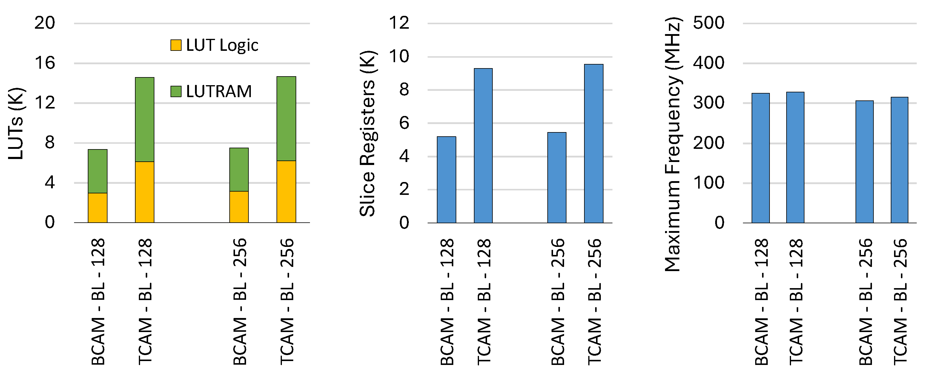
Figure 10. While LUTRAM usage follows the same trend as in the BF mode, LUT logic consumption in TCAM is approximately 98% and 108% higher than in BCAM for depths of 128 and 256, respectively. This increase is attributed to the semi-parallel processing approach in the BL mode, which requires additional logic to handle and schedule the partitioned block memory units. Registers are also increasingly demanded for the TCAM to store more and wider intermediate signals in the pipeline. Despite these differences, the maximum operating frequencies of both architectures remain within a similar range.
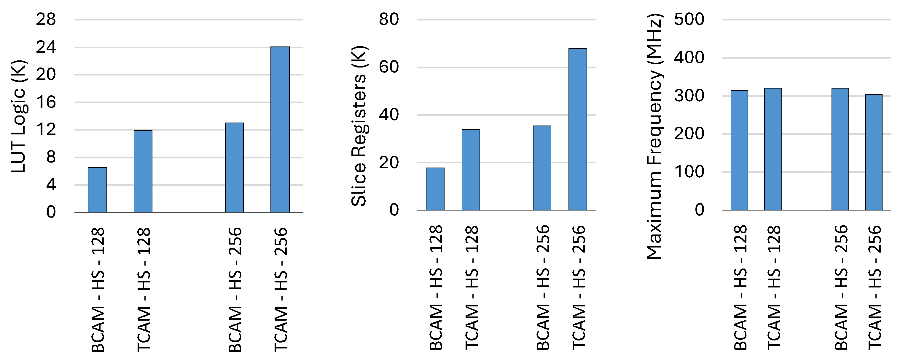
Figure 11 presents the comparison in HS mode, where LUTRAM is no longer used, making registers the primary resource for storage. The LUT logic and register utilization trends in HS mode follow the same pattern as in BL mode, but with higher overall values due to the increased parallelism and partitioning required for high-speed operation. The maximum clock frequency follows a similar trend to BL mode, varying from 300 MHz to 320 MHz.
5.4. High-Speed (HS) Optimization Mode Variations
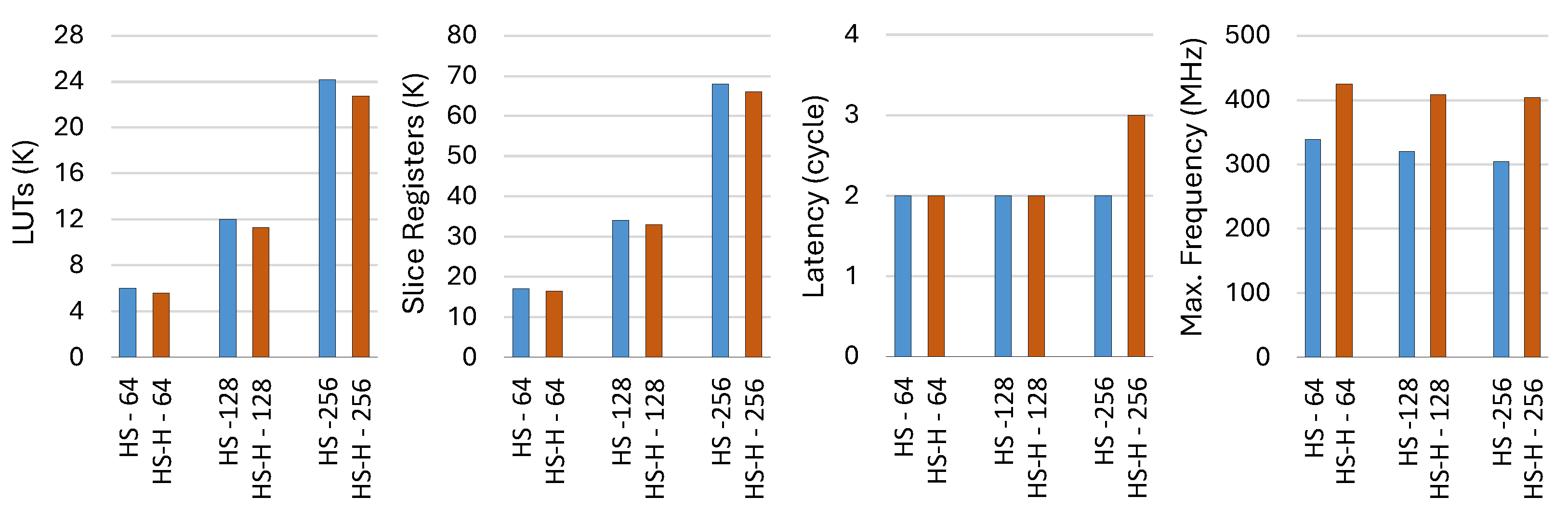
Furthermore, we compare the HS mode and its enhanced version, HS-H mode, across different CAM depths for the proposed TCAM design.
Figure 12 presents a detailed comparison of resource utilization, latency, and maximum clock frequency for both modes, using TCAM configurations with depths of 64, 128, and 256, while keeping the key width fixed at 128 bits. The results demonstrate that the HS-H mode achieves up to 7% higher efficiency in LUT utilization and up to 4% higher efficiency in register utilization compared to the HS mode. The most significant improvement is observed in the maximum clock frequency, which increases by up to 32.9% for a TCAM depth of 256. However, as expected, the latency increases by one cycle when the TCAM depth is 256.
5.5. Comparison
To evaluate the proposed HLSCAM architectures, we consider the HS-H mode, which offers improved resource efficiency and higher operating frequencies compared to the HS mode. The comparison considers key performance metrics, including FPGA resource utilization, which accounts for the combination of LUTRAMs, LUT logic, slice registers, maximum clock frequency, and throughput. Throughput
is defined as the rate of lookup operations completed per second, which is measured in bits per second (bps) and calculated using Equation (
3) [
11]:
where the
is the maximum frequency and
is the key width of the CAM. Since CAM architectures in the literature are implemented on different FPGA devices, a normalized throughput (N.TP) metric is introduced to allow for a fair comparison. It is defined in Equation (
4) [
11]:
where
is a coefficient that compensates for differences in FPGA technology speed, making performance metrics more comparable across different devices. The
is computed using Equation (
5) [
11]:
where
refers to the FPGA CMOS technology size and the
refers to the corresponding supply voltage. The Virtex-6 family is used as the baseline FPGA, as it is fabricated with a 40 nm process and operates at 1.0 V supply voltage.
Table 3 lists the related FPGA parameters used to calculate the normalized throughput. It provides the relevant FPGA parameters, including those for Virtex-6, Kintex-7, Virtex-7, and Virtex Ultrascale+, enabling the calculation of scaling factors for each. The comparison results are compiled to reflect post-place-and-route implementations.
Table 4 shows the results of the proposed HLSCAM architectures in the HS-H mode and other existing work. The comparison results are obtained after post-place-and-route implementation for both Virtex-7 (xc7v2000tflg1925-2) and Virtex Ultrascale+ (xcu280-fsvh2892-2l-e). Resource usage is reported in terms of LUTs, FFs, and BRAMs. Additionally, CLBs (Configurable Logic Blocks) are used for Virtex UltraScale+ device, while Slices are reported for older FPGA families. The
and
represent the throughput and normalized throughput, respectively. However, a direct quantitative comparison is still challenging, as not all works report the same set of resource utilization metrics, as well as variations in FPGA devices, synthesis tools, and experimental setups. Additionally, since each FPGA slice contains multiple LUTs and registers, comparing slices alone does not fully reflect differences in resource efficiency across different architectures. Despite these challenges, a qualitative comparison is made by analyzing key performance characteristics.
Some existing TCAM implementations, such as Scalable TCAM and Zi-TCAM, report high slice usage, whereas the proposed architectures demonstrate more efficient resource allocation while achieving significantly higher operating frequencies. Unlike Z-TCAM and UE-TCAM, which rely on BRAM-based storage, the proposed architectures avoid BRAM dependency, improving scalability for high-speed large CAM sizes. Since the HLSCAM uses high-level partitioning, particularly in the HS mode, using BRAM would lead to underutilized memory blocks.
The proposed HLSCAM architectures achieve higher maximum operating frequencies than most existing designs, such as Hierarchical TCAM (109 MHz), Zi-TCAM (38 MHz), and HP-TCAM (118 MHz). Compared to G-AETCAM, which operates at 358 MHz, the proposed TCAM architecture sustains competitive clock speeds while handling larger key widths and CAM depths. Compared to D-TAM, the corresponding HLSCAM configuration exhibits slightly lower operating frequency, resulting in lower throughput. Nevertheless, in the wider CAMs such as , the HLSCAM achieves up to 31.18 Gbps normalized throughput.
For similar CAM sizes, HLSCAM achieves higher operating frequencies than Xilinx CAM IPs. For TCAM , HLSCAM runs at 404 MHz versus 316 MHz. For TCAM , it operates at 365 MHz compared to 323 MHz. This results in greater normalized throughput 24.30 Gbps versus 19.04 Gbps and 6.12 Gbps versus 5.47 Gbps. However, Xilinx CAM IPs use BRAM for balanced resource utilization, while HLSCAM relies on distributed memory, increasing CLB usage.
Although HLSCAM TCAM and BCAM consistently achieve significantly higher maximum frequencies and related throughput than most existing works, the resulting normalized throughput gains are not proportionally higher. This is due to the scaling factor introduced by the normalization equation, which is not ideal for accurately reflecting performance improvements across different architectures and configurations.
6. Discussion
The proposed HLSCAM framework introduces a flexible, high-performance CAM implementation in HLS, enabling users to define their CAM table sizes according to specific application requirements. Unlike fixed hardware designs, this adaptability allows for customized trade-offs between resource utilization and performance, making it a versatile solution for FPGA-based packet processing.
To further enhance flexibility, HLSCAM provides multiple optimization strategies, offering users a range of configurations to balance throughput, latency, and resource consumption. The three primary operational modes (BF, BL, and HS) are designed to meet diverse performance demands. The BF mode is particularly suited for resource-constrained scenarios, offering a highly compact implementation. In contrast, the HS mode prioritizes minimal latency by leveraging parallel registers at the cost of higher resource consumption. The BL mode provides a balanced trade-off between latency and resource efficiency through partitioning memory blocks into multiple LUTRAMs. The parameter plays a critical role in this trade-off, acting as a control knob to shift the design towards either a resource-efficient or low-latency CAM table.
Furthermore, we introduced an improved version of the HS mode, termed HS-H, which retains the fundamental parallel processing benefits of the HS mode but adopts a hierarchical structure. This architectural enhancement significantly reduces intermediate signal propagation, leading to up to 7% LUT reduction and up to 4% reduction in register utilization, while also achieving up to 32.9% improvement in maximum operating frequency.
HLSCAM is specifically tailored for dataplane packet processing, distinguishing it from traditional CAM architectures. The entry format is adapted to accommodate network rule storage, incorporating a valid bit to determine entry validity and a value field for packet processing upon a successful match. For TCAM implementations, mask bits are explicitly defined for the entire key width, leading to higher memory consumption compared to conventional CAM solutions. As a result, for the same CAM dimensions, HLSCAM requires more than double the memory units used in existing works.
Despite its relatively higher FPGA resource consumption, HLSCAM outperforms many competitors in terms of frequency and throughput, particularly in the configuration. Additionally, it delivers substantial throughput in configurations such as and . A key factor contributing to HLSCAM’s resource consumption is its HLS-based implementation. Unlike HDL-based solutions, which allow fine-grained control over hardware resources, HLS-based designs introduce abstraction layers that can lead to additional overhead. While this abstraction enhances design flexibility, it often results in less efficient resource utilization than RTL implementations. This inefficiency becomes more pronounced in larger designs that rely on deep pipelining, where mapping high-level behavioral code to FPGA logic and memory introduces complexity. One way to mitigate this issue is to reduce memory partitioning, simplifying the design to lower memory and logic overhead. A hybrid approach that combines semi-partitioned memory with a hash-based lookup scheme could further optimize resource efficiency by reducing the number of required comparisons. However, potential hash conflicts must be carefully considered. Investigating the feasibility and effectiveness of these approaches, along with their impact on resource utilization and lookup performance, remains an area for future research.
Nevertheless, HLSCAM enables the easy generation of arbitrary CAM configurations, while automatic scheduling mechanisms optimize logic placement and pipelining to achieve high operating frequencies. These features are beneficial for high-speed networking and packet processing applications, including rule-based packet flow filtering, Intrusion Detection Systems (IDS), In-band Network Telemetry (INT), timestamping, and packet classification.
7. Conclusions
This paper presented HLSCAM, a fine-tuned HLS-based implementation of BCAM and TCAM for high-speed packet processing on FPGAs. By leveraging High-Level Synthesis, the proposed approach enables configurable, scalable, and resource-efficient CAM architectures, reducing development complexity compared to traditional RTL-based implementations. The design methodology employed different design parameters to provide a fine-tuned FPGA parallelism management. This approach, combined with a structured implementation, allowed the synthesis tool to decrease the critical path. The Brute Force (BF), Balanced (BL), and High-Speed (HS) modes offer a spectrum of design trade-offs between latency, resource utilization, and throughput, allowing customization for different networking applications.
The evaluation results demonstrated that HLSCAM achieves significantly higher operating frequencies than most existing FPGA-based CAM designs, reaching up to 423 MHz. The HS mode achieved the lowest lookup latencies, while the BL mode provided a balance between resource efficiency and performance. Despite higher resource consumption due to extensive partitioning and parallelism, the proposed architectures delivered competitive throughput across various configurations. A comparison with previous work highlighted HLSCAM’s advantages in flexibility, scalability, and high-speed performance, particularly in large-scale CAM applications. By avoiding BRAM dependency, the proposed architectures improve scalability, making them well-suited for high-performance packet classification and filtering.
Future work will further optimize HLS-based CAM architectures to save resources while maintaining rapid lookup. Approaches like hash-based methods could prevent CAMs from comparing with all entries to reduce logic and the need for memory partitioning, thereby improving efficiency. Additionally, integrating these CAMs into real-world network processing pipelines will provide further insights into their applicability in next-generation networking systems.


