Article

Package Integration and System Performance Analysis of Glass-Based Passive Components for 5G New Radio Millimeter-Wave Modules

by
Muhammad Ali
1,*,†,
Atom Watanabe
2,†,
Takenori Kakutani
3,†,
Pulugurtha M. Raj
4,
Rao. R. Tummala
5,† and
Madhavan Swaminathan
6,†
1
Apple Inc., 1 Apple Park Way, Cupertino, CA 95014, USA
2
IBM Corporation, 1 New Orchard Road, Armonk, NY 10504, USA
3
Taiyo Ink Mfg. Co., 900 Oaza-Hirasawa Ranzan-Machi Hiki-Gun, Saitama 355-0215, Japan
4
Department of Biomedical Engineering, Florida International University, Miami, FL 33174-1630, USA
5
Department of Electrical and Computer Engineering, Georgia Institute of Technology, Atlanta, GA 30332, USA
6
Department of Electrical Engineering, Pennsylvania State University, University Park, PA 16802, USA
*
Author to whom correspondence should be addressed.
This research work was performed at Georgia Institute of Technology by these authors.
Electronics 2025, 14(8), 1670; https://doi.org/10.3390/electronics14081670
Submission received: 17 March 2025 / Revised: 31 March 2025 / Accepted: 14 April 2025 / Published: 20 April 2025
(This article belongs to the Section Microwave and Wireless Communications)

Abstract

:
In this paper, package integration of glass–based passive components for 5G new radio (NR) millimeter–wave (mm wave) bands and an analysis of their system performance are presented. Passive components such as diplexers and couplers covering 5G NR mm wave bands n257, n258 and n260 are modeled, designed, fabricated and characterized individually along with their integrated versions. Non–contiguous diplexers are designed using three different types of filters, hairpin, interdigital and edge–coupled, and combined with a broadband coupler to emulate a power detection and control circuitry block in an RF transmitter chain. A panel–compatible semi–additive patterning (SAP) process is utilized to form high–precision redistribution layers (RDLs) on laminated glass substrate, onto which fine features with tight tolerance are added to fabricate these structures. The diplexers exhibit low insertion loss, low VSWR and high isolation, and have a small footprint. A system performance analysis using a co–simulation technique is presented for the first time to quantify the distortion in amplitude and phase produced by the fabricated passive component block in terms of error vector magnitude (EVM). Moreover, the scalability of this approach to compare similar passive components based on their specifications and signatures using a system–level performance metric such as EVM is discussed.

1. Introduction

Highly integrated solutions for modern radios promise higher data rates, smart utilization of the spectrum, functional density and energy efficiency by solving specific hardware– and software–related challenges to enhance wireless communication networks [1,2]. The grand vision of 5G to provide diversity in terms of services, the spectrum and deployments has opened new technological challenges which need to be addressed. Enhanced mobile broadband (eMBB), ultra–reliable low–latency communication (URLLC) and massive machine–type communication (mMTC) are the three use–cases of the 5G air interface. Hardware–level implementation of these use–cases relies on the heterogeneous integration of antenna arrays and active and passive devices as one of the key enabling technologies for the next generation of radio solutions such as 5G new radio (NR) [3,4,5].
Increased path loss with higher operating frequencies such as 5G mm wave bands requires the use of directed communication to provide Gb/s data rates with high fidelity and low latency. Antenna–in–package (AiP) architecture is almost universally sought for all 5G applications such as user equipment (UE), customer premises equipment (CPE) and base–stations [6,7,8,9]. The research and development in this area has fueled many breakthroughs in related primary and auxiliary technologies, particularly for 5G NR mm wave applications. Specifically, integrating phased arrays in packages poses challenges such as increased complexity and reduced thermo–mechanical reliability, leading to the co–design of passives, ICs and antenna elements [10]. Understanding the system–level specifications and translating them to IC–, package– and component–level requirements can aid in achieving a faster time to market [11]. A cross-section of a modern 5G module with broadband and/or an end–fire antennas is shown in Figure 1. Heterogeneously integrated active and passive components along with high–density layers for digital routing and low–loss, seamless interconnects are key features of this glass–substrate–based module.
Implementation on LTCC and organic substrates results in fundamental limitations to achieving high–precision sub–micron features with tight tolerance. Traditional RF passive components and substrates use low-temperature co–fired ceramic (LTCC) technology, which involves multiple layers of ceramic and copper. This mature technology is common in industry for passive components and RF FEMs. However, due to limitations in terms of thickness reduction and scalability to the panel level, LTCC has been surpassed by multilayer organic laminate substrate technology. These organic laminates are popular due to their low cost, ease of processing and large panel manufacturing. They also allow the integration of multiple chips in the same package, increasing functional density and performance while reducing costs. However, organic laminates fall short of miniaturization requirements for emerging electronics, particularly for 3D architectures.
Glass–based packaging has emerged as a potential solution to address the limitations of low–temperature co–fired ceramic (LTCC) and organic substrates, as it is advantageous in terms of benefits such as silicon-like dimensional stability, a tunable coefficient of thermal expansion (CTE), low–loss through–glass vias (TGVs), panel–scale processability and the ability to support fine-feature redistribution layers (RDLs) as a result of low–loss polymer dielectric lamination. Copper can be precisely patterned using a semi–additive patterning (SAP) process on these RDLs. Since the CTE of glass is tunable (3–8 ppm/K), it can be matched to silicon dies for ease of assembly and improved reliability. This provides engineers with a new horizon to explore the flexibility of the electrical and mechanical properties of laminated glass substrates for 5G and mm wave modules. Glass–based packaging solutions for 5G and mm wave applications are widely pursued in academia [12,13] and industry [14,15].
This paper presents the packaging implementation and a system performance analysis of glass–based integrated passive components for 5G NR mm wave modules. The bands of interest are in frequency range 2 (FR2), as defined by 3GPP: n257, n258 and n260 [16,17]. The frequency range and fractional bandwidth (FBW) of each band are as follows: n257: 26.5–29.5 GHz (10.71%); n258: 24.25–27.5 GHz (12.6%); and n260: 37–40 GHz (7.8%). It is to be noted that band n261 is a subset of band n257, with a frequency range of 27.5–28.35 GHz (3.04%). This study includes miniaturized mm wave diplexers, a broadband coupler, and an integrated passive component block combining both.
This integrated passive component block finds its place in a power detection and control circuitry in a modern RF power amplifier (PA) front–end module (FEM), a schematic diagram of which is shown in Figure 2, and it is used as an example in this work [18]. It consists of an amplifier block in conjunction with a diplexer, a directional coupler with a detector and an antenna array. It is typically used in WCDMA and GSM/EDGE systems due to their output power control requirements, especially under mismatched–load conditions [19,20]. The matching network blocks represent output matching of the amplifiers, and can be formed of LC components, transmission lines, isolators or transformers depending upon the application requirements. The filters in the diplexer act as harmonic filters, and they combine the signals coming from 28 and 39 GHz band amplifiers. The coupler can have a variable or fixed coupling factor depending upon the required level of control over the output power. The transmitter chain in Figure 2 is used to quantify the distortion of the fabricated block as well as to discuss a co–simulation approach to compare passive components using system–level performance metrics such as error vector magnitude (EVM). The choices of modulation schemes are π /4 differential quadrature phase shift keying ( π /4 DQPSK) and 64–state quadrature amplitude modulation (64–QAM), but any desired modulation scheme can be used.
Previously, the authors have published work on individual passive components such as filters [21,22,23], power dividers [24,25] and others [26,27] for 5G and mm wave applications. Unlike in [21,22], which introduces miniaturized filters covering entire 28 and 39 GHz bands, the focus of this work is on diplexers using filters for 5G NR bands (n257, n258 and n260) and their integration with couplers to implement a passive component block in an RF transmitter chain. The filters, used as building blocks for diplexers, are also designed with several design– and process–level considerations to further improve model–to–hardware correlation: cross–correlation between the simulated and measured results is improved by 5.5% when compared to the authors’ previous work. The novelty of this work is in the integration and characterization of a passive component block with advanced substrate technologies such as laminated glass, and in evaluating its system–level performance when co–packaged with other active and passive components. It serves as an intermediary step towards prototype demonstration of the integration of these filters and diplexers into an RF front–end. The system performance analysis includes power variation at the antenna port when the source power is varied and the extraction of the EVM signature of the integrated passive component block using different modulation schemes. Moreover, we present a technique based on the EVM signature of filters to discriminate them. We compare two measured filter responses obtained from the characterization of the integrated passive component block, essentially linking various component parameters to a single system–level performance metric.
This paper is organized as follows: Section 1 introduces the motivation and applications of this research. Section 2 discusses material stackup and design techniques for integrated passive components. The fabrication process details are provided in Section 3. Section 4 covers the characterization results and compares the simulated and measured results of the diplexers, couplers and integrated passive component blocks. In Section 5, the system performance analysis and EVM signature extraction of integrated passive component blocks are linked to various parameters. Finally, conclusions are drawn in Section 6.

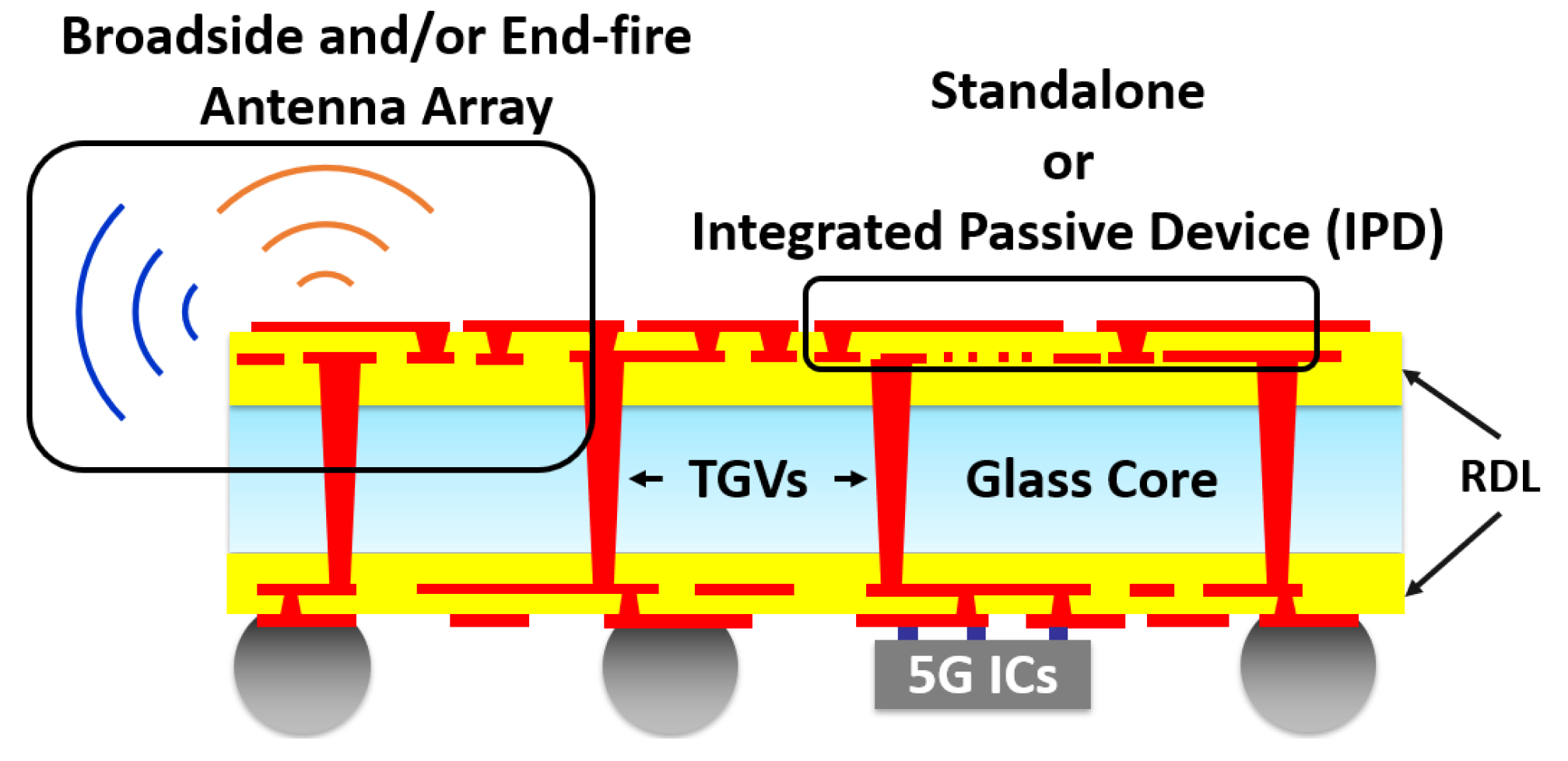
2. Design of Integrated Passive Components

In this section, we present the design of the integrated passive components. It is organized as follows: material stackup, the design of individual passive components and, lastly, their integration.

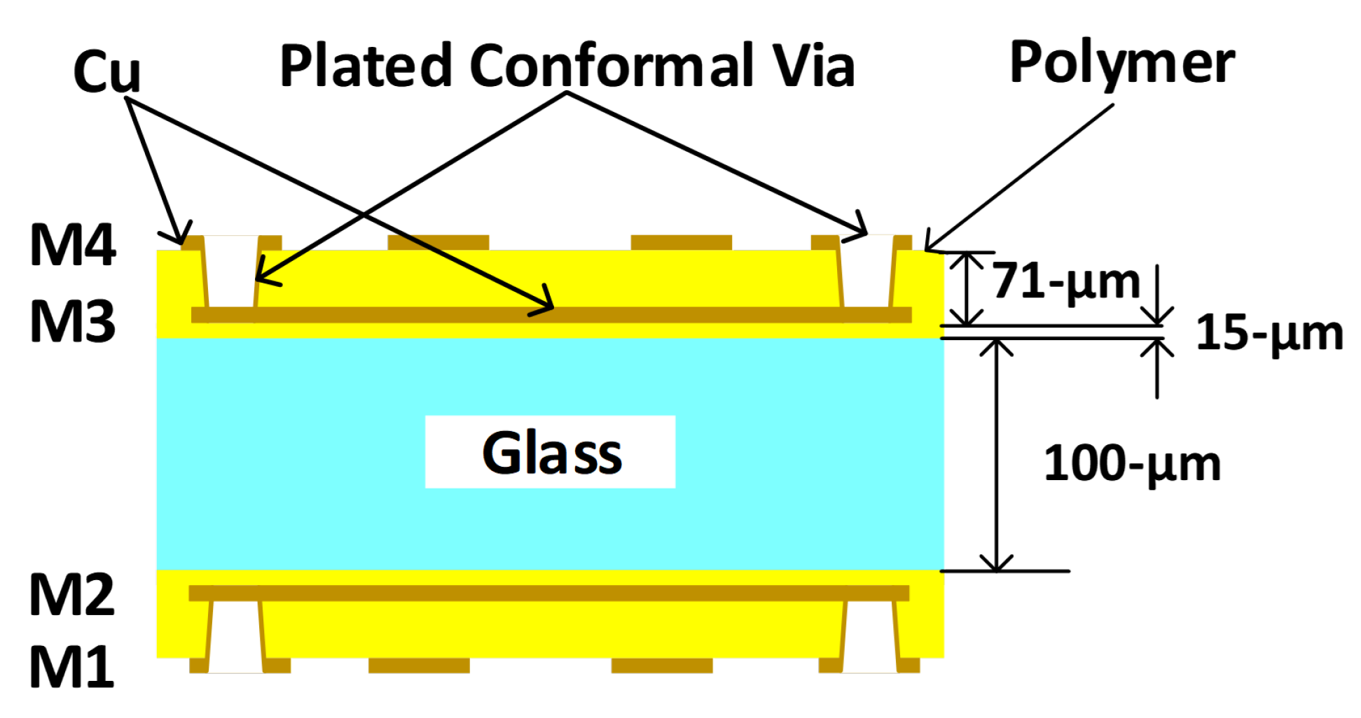
2.1. Material Stackup

A four–metal layer material stackup is selected for this demonstration, as shown in Figure 3. The core material is a 150 × 150 mm2, 100 μ m thick glass substrate (EN–A1) panel from Asahi Glass Company, Tokyo, Japan (AGC) and it has dielectric permittivity ( ε r ) of 5.4 and a loss tangent (tan δ ) of 0.005 at 10 GHz. The polymer dielectric is a low–loss epoxy film from Taiyo Ink. Mfg. Co., Saitama, Japan (ZaristoTM) with 15 μ m and 71 μ m thickness. It has ε r of 3.3 and tan δ of 0.0025 at 10 GHz. The 15 μ m thick Taiyo Zaristo is laminated onto a bare glass panel on which metal layers M2 and M3 are patterned, followed by lamination of 71 μ m Zaristo onto which M1 and M4 are patterned. M2 and M3 act as ground planes to microstrip integrated passive components on M1 and M4. The stackup is double–sided to avoid panel warpage during the fabrication process. The thickness of copper is set to 8 μ m, which is sufficiently higher than five times the skin depth at an operating frequency of 40 GHz. The total thickness of this stackup is 202 μ m.

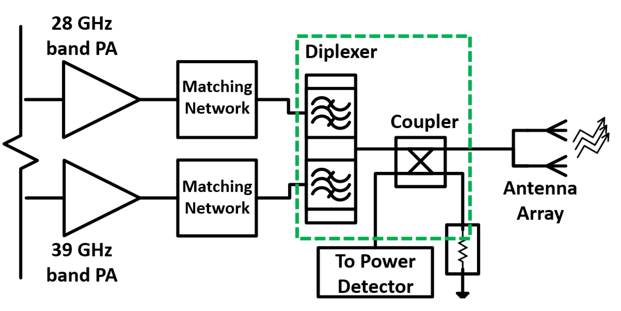
2.2. Filter, Diplexer and Coupler Design

The selection of bandpass filters for this demonstration is based on the types of resonators. Hairpin filters are designed using coupled half–wavelength ( λ /2) open–circuited stub resonators. The interdigital filters are composed of quarter–wavelength ( λ /4) short–circuited stub resonators, and edge–coupled filters are formed using parallel-coupled λ /2 resonators. Both the hairpin and interdigital filters are designed using a 0.043 dB Chebyshev equal-ripple response with fifth–order g–values, and the edge–coupled filters are designed using fourth–order g–values. All filters are doubly terminated: they have 50 Ω impedance at both ports. Their order is selected based on acceptable passband insertion loss and stopband attenuation of more than 30 dB. Hairpin and interdigital filters are designed for bands n257, n258 and n260, whereas edge–coupled filters are designed for combined bands n257 and n258 (24.25–29.5 GHz) and band n260. The design procedure for the filters is described in [21,22,28].
Since the 28 and 39 GHz 5G NR bands are separated by a frequency range of 29.5–37 GHz (not including edge frequencies), the diplexer structures for these bands are non–contiguous and can be designed using the aforementioned doubly terminated filters. A T–junction with special properties can be designed to connect two doubly terminated filters in such a way that they do not load each other and effectively appear “open” in the stopband of the other filter [29]. This configuration results in a diplexer. Using the doubly terminated filters designed for this demonstration, hairpin, interdigital and edge–coupled diplexers are designed. The simulated response of a diplexer based on interdigital filters for bands n258 and n260 and its layout are shown in Figure 4.
For the directional coupler, a passive, three–section coupled–line coupler with a 20 dB coupling factor is designed which can be connected to a power detector to measure the output power of the antenna. Since the coupling factor is 20 dB, only 1% of the power is coupled from the main line of the coupler, ensuring better signal integrity in the critical signal path to the antenna. The coupler covers the desired bandwidth of 24.25–40 GHz and has a maximum passband insertion loss of 0.35 dB with small variation in coupling in the desired frequency range. One critical condition for the constant coupling factor is the termination at the isolation port of the coupler. Variations in impedances at the coupler termination ports can lead to an undesired response, but this can also be compensated for using complex termination techniques at the isolated port, as discussed in [30]. The simulated response of the coupler along with its layout is shown in Figure 5.

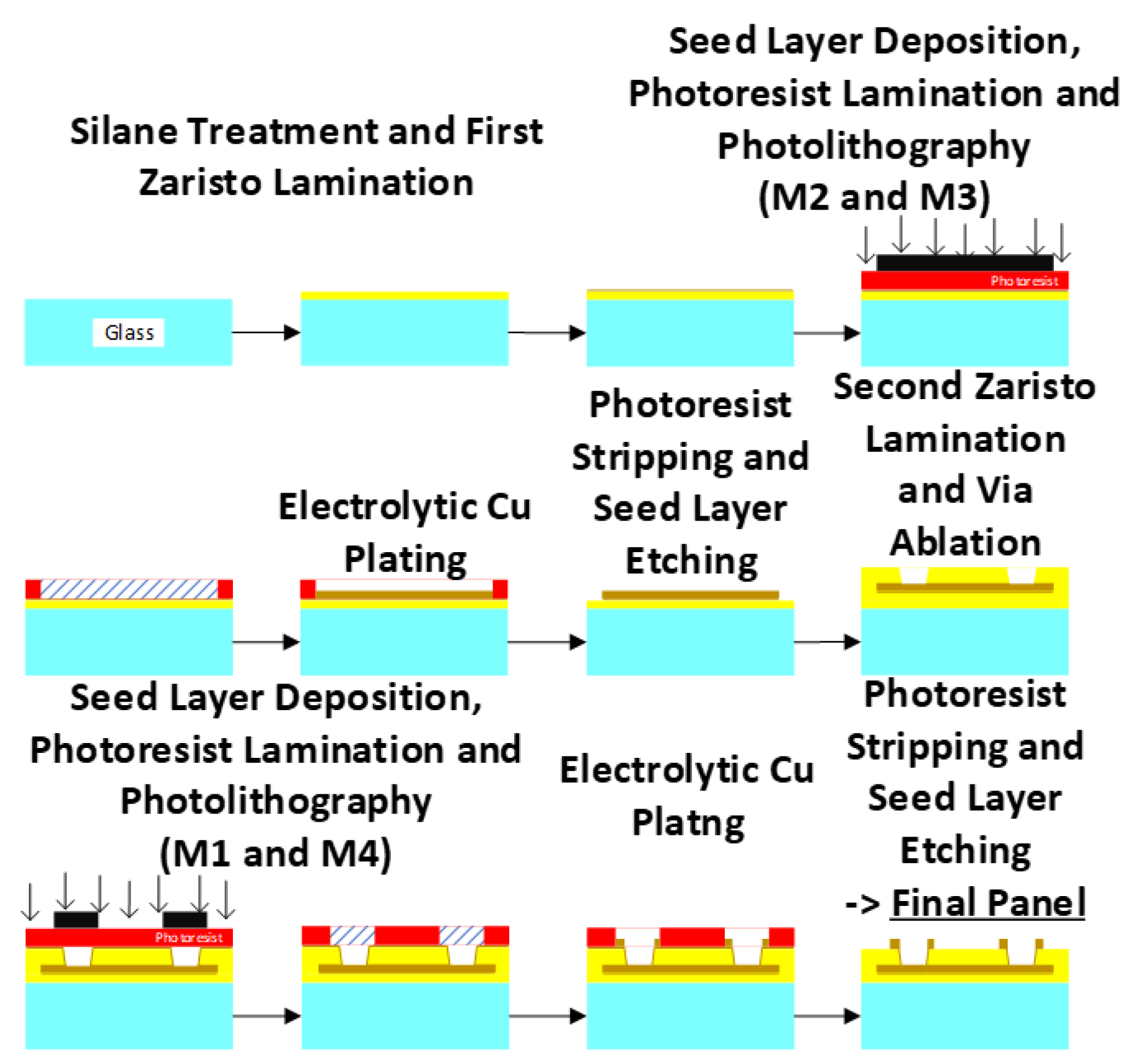
3. Fabrication Process

The semi–additive patterning (SAP) process creates fine copper patterns necessary for achieving the desired structures. Unlike conventional etching methods, SAP enhances control over the deposited copper profile, which is crucial for 5G applications [31,32]. It reduces side–wall etching and undercutting, resulting in a rectangular cross–sectional profile of the metal patterns. The process begins when silane is used to treat a bare 100 μ m glass panel to improve adhesion to polymer dielectrics and prevent delamination. At this stage, the glass is brittle, so handlers must use proper procedures. A vacuum laminator laminates a 15 μ m Zaristo layer on both sides of the glass panel, followed by a curing process. Subsequently, we carry out electroless deposition of a thin copper seed layer, followed by patterning the M2 and M3 metal layers using photolithography. We perform electrolytic plating to achieve the required copper thickness, strip the photoresistor and differentially etch the seed layer using a chemical etcher. Finally, Atotech’s Novabond process enhances the adhesion strength of Zaristo to the deposited copper by creating microscopic anchor sites [33].
The remaining fabrication process is similar to the patterning of M2 and M3 with the addition of two steps: (1) the two–step lamination of Zaristo to achieve a 71 μ m thickness, and (2) the ablation of blind vias before seed layer deposition. A step–by–step illustration of the fabrication process is shown in Figure 6. The measured copper thickness is 7.8 ± 0.5 μ m in the fabricated panel. Several coupons of various structures are shown in Figure 7, Figure 8, Figure 9 and Figure 10. Due to the constraints of measurement setup for multi–port networks, we fabricated several coupons of identical structure. The following section will explore this topic in detail.

4. Results and Discussion

We discuss the characterization results of individual and integrated passive components in this section. Our setup includes a two–port VNA with a 14–40 GHz range and 500 μ m pitch ACP40 GSG probes, using SOLT calibration. We conducted a dimensional analysis to inspect the features and determine the electrical dimensions from the physical coupons.
There are two fundamental limitations of the available measurement setup which influence the design stage. The first one is the truncation of measured data at the highest frequency of VNA (40 GHz). The second limitation, which results in an extensive and elaborate design stage, is the number of VNA ports (limited to two). Since diplexers, couplers and their integrated versions are multi–port networks, several versions of the same structure need to be designed with the remaining ports terminated using broadband terminators. In this way, a three–port network such as a diplexer requires three design variants to obtain all six s–parameters, as governed by a commonly known formula of combinations. The combination of a diplexer and a coupler leads to a five–port network which requires ten design variants for complete characterization. To maintain practicality in measurements, a few variations are designed to obtain key s–parameters, such as S21 and S42, for the combined diplexer and coupler, as shown in Figure 10. High–frequency chip resistors with a 0402 (1005 metric) footprint are chosen as the broadband terminators [34]. Some of the soldered resistors on the fabricated multi–port structures, such as diplexers, couplers and their integrated versions, are shown in Figure 11.
We fabricated the doubly terminated filters individually to characterize their response. Design and fabrication improvements ensured excellent model–to–hardware correlation. All filters (hairpin, interdigital and edge-coupled) show maximum passband insertion loss of 2.60 dB, return loss better than 15 dB and VSWR of less than 1.43. These values include 1 mm input and output feed lines. The frequency ratio at the 30 dB attenuation point to the band edge on both sides of the passband gives the stopband performance, which is less than 1.17 for hairpin filters, 1.2 for interdigital filters and 1.22 for edge–coupled filters. Figure 12 shows the simulated and measured responses of the two fabricated filters.

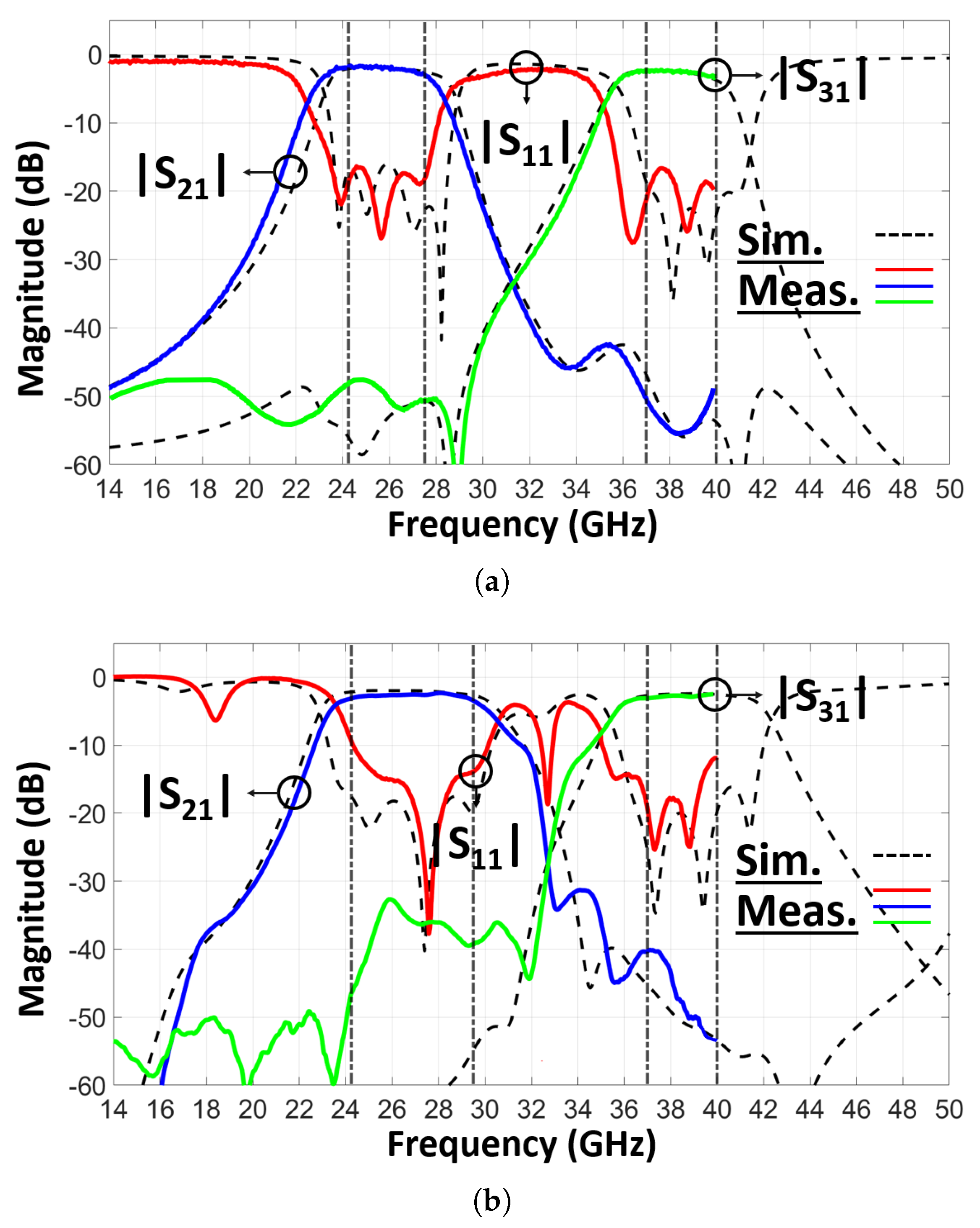
4.1. Characterization Results of Diplexers

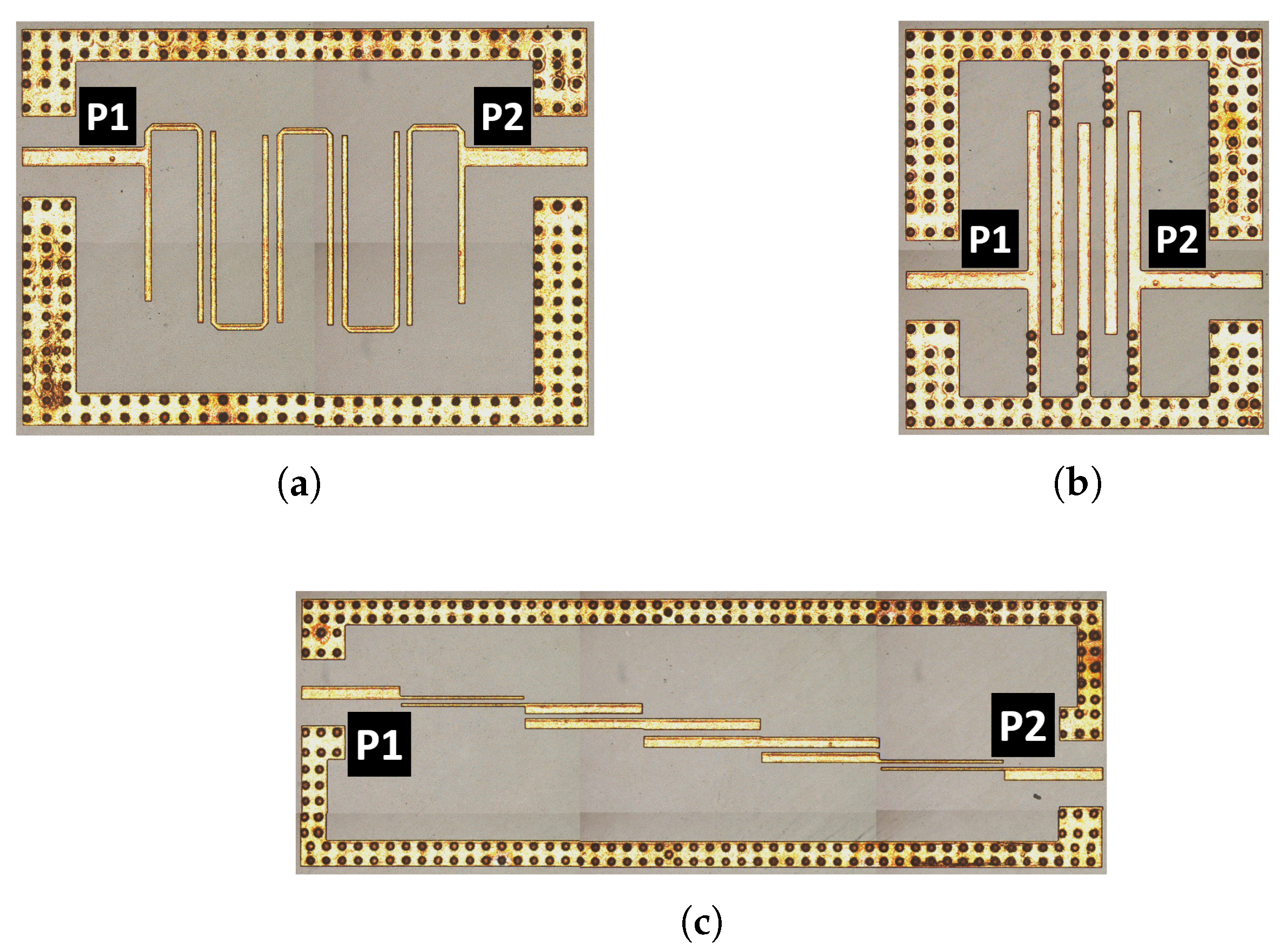
4.1.1. Hairpin Diplexers

A comparison of the simulated and measured results of the fabricated hairpin diplexers is shown in Figure 13. The s–parameters (S11, S21 and S31) are measured on separate coupons and combined with the simulated results for comparison. As evident from Figure 13, the non–ideal behavior of high–frequency resistors used as broadband terminators starts appearing in the stopband region of one filter, which has the same frequency as the passband of the other filter. This implies that the impedance of the broadband terminator is not purely resistive; rather, it has some reactance associated with it. The maximum passband insertion loss of both diplexers is 3 dB, the return loss is better than 14 dB and the VSWR is less than 1.5. The isolation between the two filters in both diplexers is better than 50 dB. The cross–over point of the hairpin diplexer (bands n257 and n260), shown in Figure 13a, is at 33.12 GHz with insertion loss of 30.6 dB. Similarly, the cross–over point is at 32.07 GHz with 37 dB insertion loss for the hairpin diplexer (bands n258 and n260), as depicted in Figure 13b.

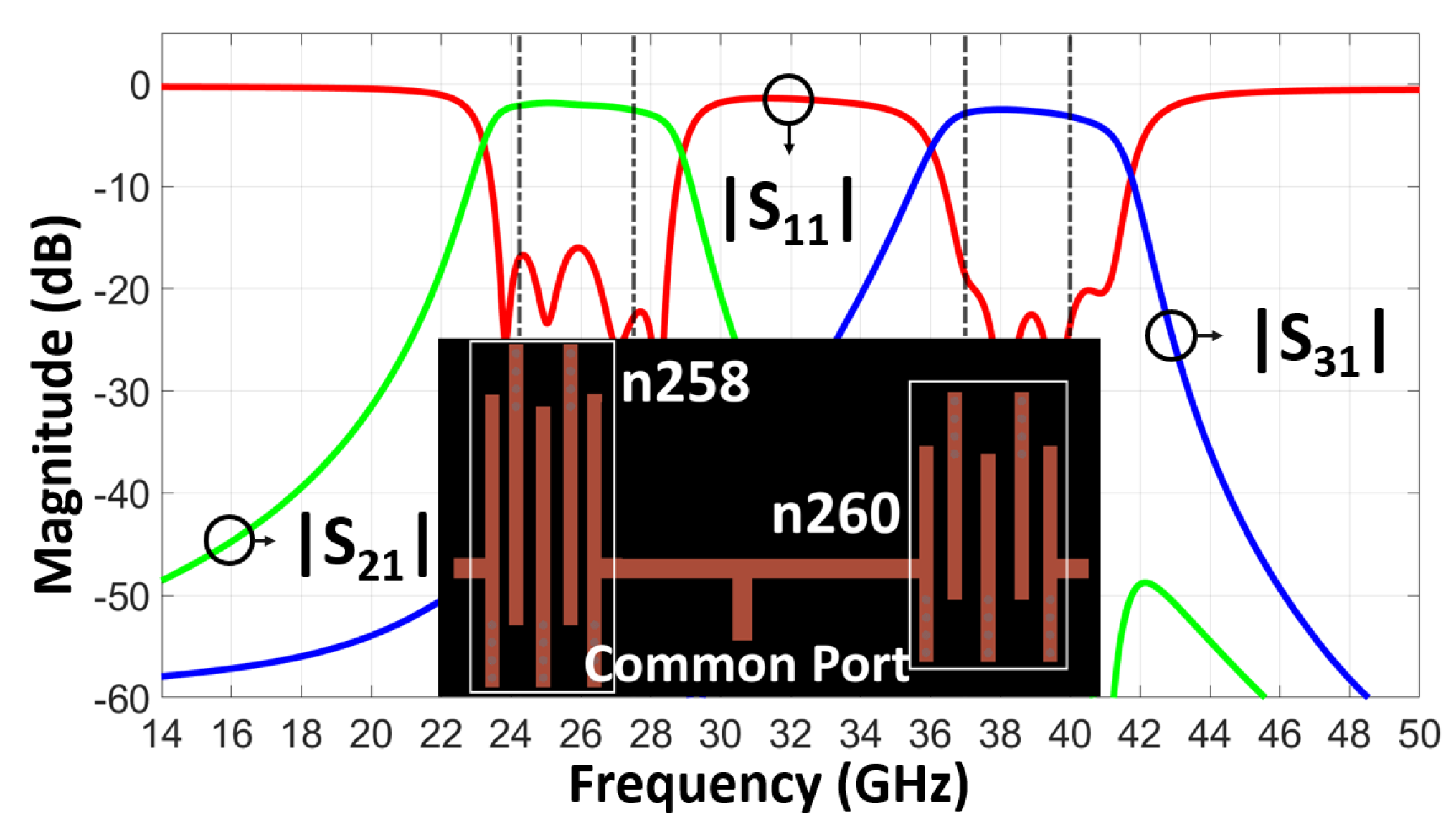
4.1.2. Interdigital Diplexer

A comparison of the simulated and measured results of the interdigital diplexer for bands n258 and n260 is shown in Figure 14a. Its insertion loss, return loss and VSWR are similar to those of hairpin diplexers. The isolation between the two filters is better than 45 dB, and the cross–over point is at 31.43 GHz, with 34 dB insertion loss.

4.1.3. Edge–Coupled Diplexer

A comparison of the simulated and measured results of the edge–coupled diplexer for combined bands n257 and n258, and n260, is shown in Figure 14b. The maximum passband insertion loss of this diplexer is 3 dB, the return loss is better than 14.3 dB and the VSWR is less than 1.48. The isolation between the two filters is better than 40 dB. The cross–over point of both filters is at 32.73 GHz, with insertion loss of 27 dB.

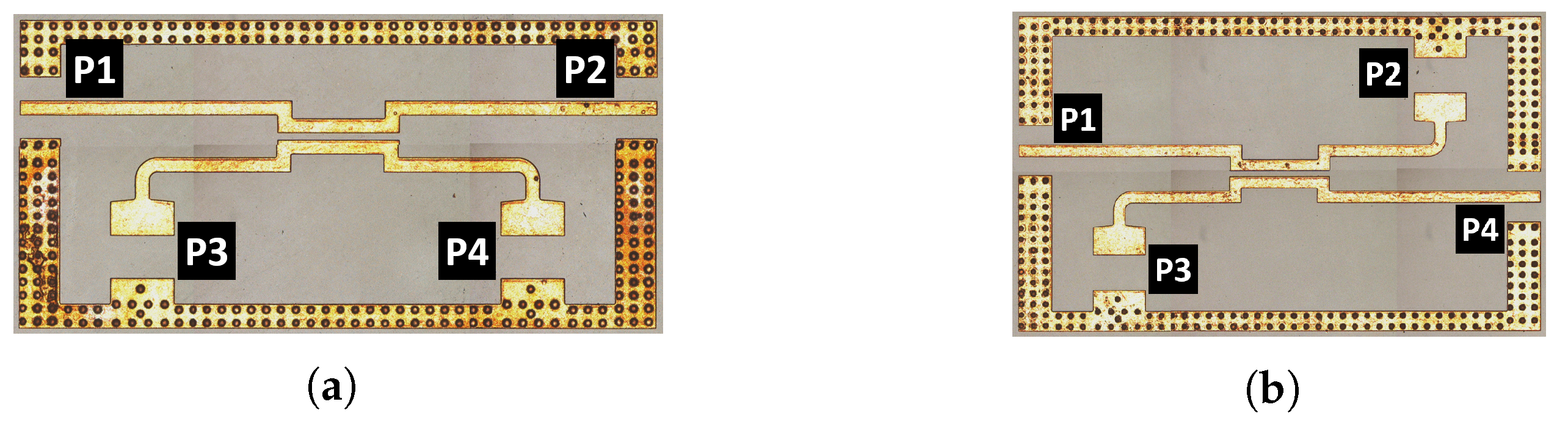
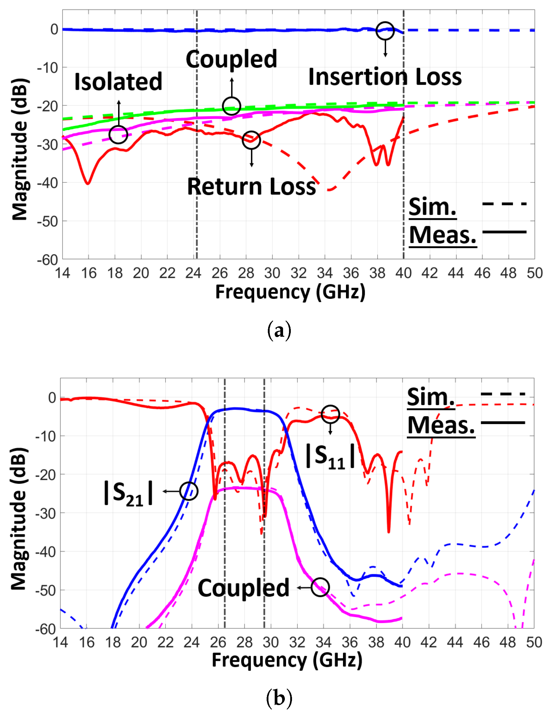
4.2. Characterization Results of Coupler and Integrated Passive Component Block

A comparison of simulated and measured results of the coupled–line coupler covering the 24.25–40 GHz frequency range is shown in Figure 15a. The maximum measured insertion loss of the coupler in the entire frequency range is 0.4 dB, the return loss is better than 20 dB and the coupling is about 20 dB with small variation.
Similarly, for the fabricated integrated passive component block in Figure 10, only two paths are measured: the band n257 filter in the diplexer to the antenna port, and the band n257 filter to the coupled port of the coupler. All additional line lengths to accommodate ease of testing are de–embedded to obtain the results shown in Figure 15b.

4.3. Dimensional Analysis

Table 1 presents the physical and electrical dimensions of some fabricated structures. We normalize the electrical dimensions according to the free–space wavelength ( λ 0 ) at the operating frequency. For the 28 GHz 5G band (24.25–29.5 GHz), we use f c as 26.875 GHz with a λ 0 of 11.16 mm. For the 39 GHz band, we use f c as 38.5 GHz with a λ 0 of 7.8 mm. For the diplexers and integrated versions, we use the 24.25–40 GHz band with a λ 0 of 9.34 mm. Table 2 compares filters that use various substrate technologies for mm wave applications, highlighting laminated glass–based filters as compact IPD structures. Table 3 compares diplexers regarding center frequency ( f c L and f c H ), bandwidth, insertion loss and size.

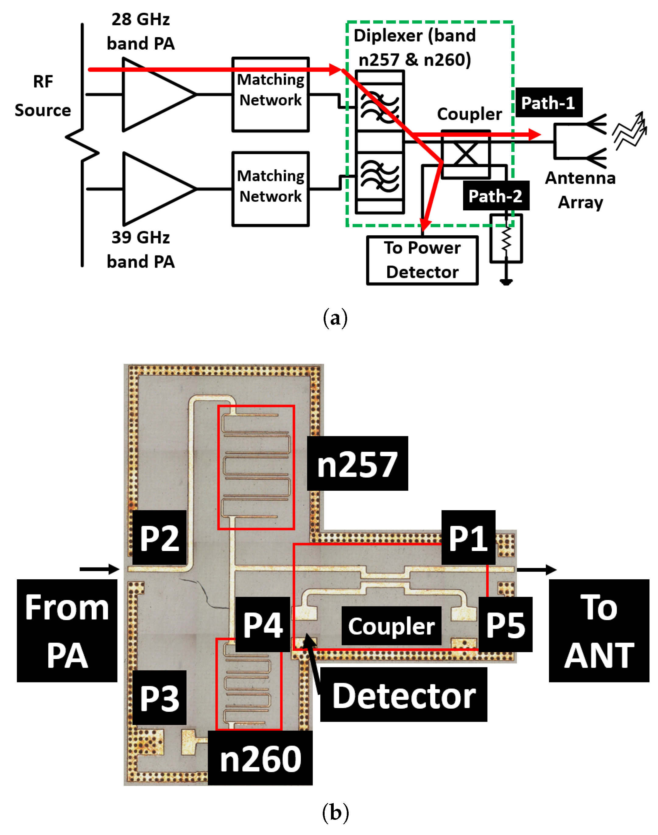
5. System Performance Analysis

In this section, a system–level performance analysis for the integrated passive component block is presented. The purpose of these co–simulations is to provide insights into the system performance of components in an RF chain and to provide accuracy in the link budget and operation range analyses [46]. The integrated passive component block shown in Figure 10 is selected for these simulations as two-port measurements are performed to characterize two critical paths:– Path–1: RF Source –> PA –> Diplexer (band n257) –> Coupler (Thru) –> Antenna Input; Path-2: RF Source –> PA -> Diplexer (band n257) –> Coupler (Coupled) –> Power Detector. These paths are highlighted in Figure 16a, and they can be corroborated with the integrated passive component block as shown in Figure 16b. The following system–level simulations are performed to quantify the distortion caused by this block:
  • Group delay variation at antenna port and power variation at detector port of system as RF source power is varied.
  • EVM of integrated passive component block using RF carrier modulated by π /4 DQPSK and 64–QAM.
To perform these simulations, a suitable PA with a 24 to 34 GHz range of operation and 23 dB gain is selected and modeled in Keysight ADS 2019 [47]. Also, it is assumed that all terminating impedances, such as at the antenna and detector port, are 50 Ω . The PA is modeled in Keysight ADS along with rest of the components to form a transmitter chain. The component impedances, especially for the PA, are optimized for better operation of the PA rather than 50 Ω , and thus, the impedances of the components at the PA output can affect its loading. The nature of the output matching network of the PA plays a critical role in design fidelity. This is usually dealt with using system–defined constraints and simulations earlier in the design cycle.Moreover, the non–linearities of local oscillators, frequency upconverters and the PA itself are sources of aberrations in a system and require extensive modeling of each component to set an expectation of system performance.

5.1. System–Level Simulation # 1

For this simulation, the group delay in Path–1 and power variation in Path–2 are extracted as the amplifier is driven into compression with the frequency sweep from 22 to 34 GHz. The group delay is shown in Figure 17a. As evident from the figure, the peak group delay in Path–1 is about 700 ps when the input power to the amplifier is 0 dBm. Also, the group delay contribution from the standalone amplifier is about 250–300 ps which leads to a 400 ps contribution from the integrated passive component block. This 400 ps group delay is comparable to state–of–the–art filters in industry: TDK ∼250 ps [48], Knowles >400 ps [49] and >1000 ps [50]. The RF source power is varied from 0 to 20 dBm with the step size set to 5 dBm. The power variation at the detector port is recorded and it is given by (1):
P D e t . ( dBm ) = P R F _ i n ( dBm ) + G a i n A m p . ( dB ) L o s s D i p . ( dB ) C ( dB )
where P R F _ i n is the power level of the RF source, G a i n A m p is the amplifier gain, L o s s D i p . is the insertion loss of the band n257 filter in the diplexer and C is the coupling factor of the coupler. The amplifier is driven into saturation when P R F _ i n reaches 8 dBm, and afterwards, it operates in compression. The power at the detector port saturates as the RF source power is increased, as observed in Figure 17b. A peak power detector can be used to track power variation to form a feedback loop to control the output power of the PA.

5.2. System–Level Simulation # 2

The performance of a digital communication system is typically estimated with the bit error rate (BER), signal–to–noise ratio (SNR) and EVM [51]. EVM is defined as the magnitude of the difference between a complex transmitted data symbol and its ideal counterpart. It is a figure of merit of transmission accuracy and is primarily a quantity of concern in link budget analyses of transceivers [52,53]. Relating EVM to individual component performance is a challenging task [54]. In addition to the worst–case EVM for π /4 DQPSK– and 64–QAM–modulated signals, a technique is presented in this section to characterize the EVM of Path–1 in Figure 16a and demonstrate how it is related to the component parameters. Before calculating the EVM for 5G NR radio transmission and reception in practice, the measured waveform is corrected by sampling the timing offset, RF frequency offset, removal of carrier leakage and equalization in the receiver. The EVM level of each NR carrier for 5G is specified by 3GPP: QPSK at 17.5% and 64QAM at 8%, respectively [17,55].
The ideal and distorted constellations of the 28 GHz RF carrier modulated by π /4 DQPSK are shown in Figure 18. EVM includes the effects of the non–linearity of the diplexer, coupler and PA in this case. The symbol rate is set equal to the bandwidth of the band n257 filter (3 GHz). Its total EVM is 2%, out of which 0.1% is contributed by the amplifier. The remainder is the EVM signature of the integrated passive component block. It is to be noted that the source power is set to 0 dBm so that the amplifier operates in linear region. Similarly, the ideal and distorted constellations of the 28 GHz RF carrier modulated with a 64–QAM signal and a 3 GHz symbol rate are depicted in Figure 19. For this case, the total EVM is 5.6%, which meets the 3GPP specification.

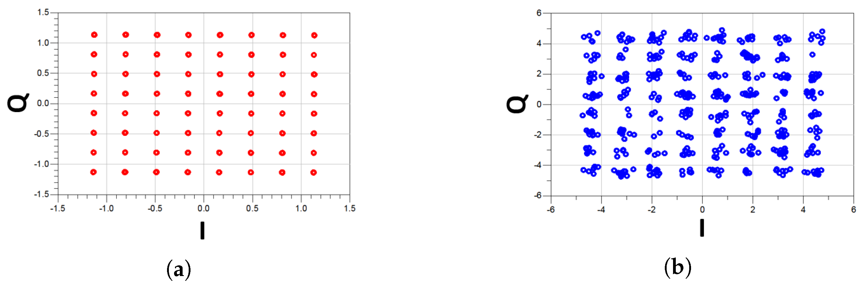
5.3. Relationship Between Component Parameters and EVM

A sweeping RF carrier frequency with a variable symbol rate can give an insight into the effects of various component design parameters on the EVM [56]. The methodology presented here can be scaled to extract EVM contributions with various modulation sources in conjunction with the performance metrics of mm wave filters, diplexers and other passive components [57]. To assess the effect of filter characteristics on EVM, we employ the following methodology:
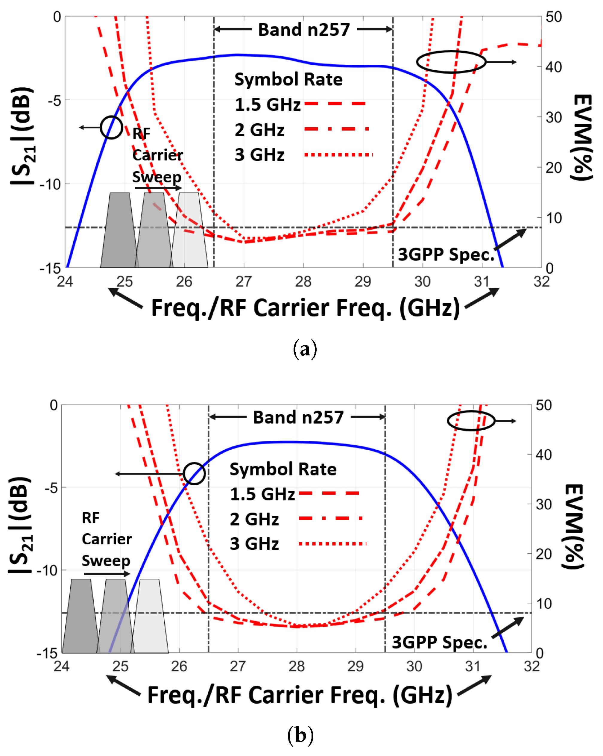
  • Sweep a 64–QAM–modulated RF carrier with 1.5, 2 and 3 GHz symbol rates over the passband of two filters (A and B) for band n257 (Figure 20).
  • The filters have different bandwidths, roll offs and ripple characteristics.
  • As the symbol rate increases, the EVM rapidly degrades, especially near the band edge.
  • Filter A shows low EVM variation ( Δ EVM < 2.3% at 1.5 GHz) with a minimum EVM of 5.6%.
  • Filter B has a minimum EVM of 5.2% and Δ EVM < 1.9%, indicating the impact of a lower ripple compared to Filter A.
  • The rejection roll–off of filters influences the asymmetric EVM response.
Highlighting the sensitivity of EVM to ripple, bandwidth and roll–off factors underscores the utility of this methodology in linking filter parameters to system performance and defining component specifications.

6. Conclusions

Package integration and a system performance analysis of ultra–thin glass–based passive components for 5G NR mm wave bands are presented. Diplexers and couplers covering bands n257, n258 and n260 are modeled, designed, fabricated and characterized. Hairpin, interdigital and edge–coupled filters are selected for diplexers, and a three–section coupled–line structure is utilized to establish the directional coupler. The panel–scale SAP process is optimized to fabricate these structures on a four–metal–layer stackup. The methodology for their characterization is also discussed, and a dimensional analysis is performed to extract their electrical dimensions from their physical dimensions. Individual filters and diplexers exhibit low insertion loss, low VSWR and high isolation, and the coupler covers the entirety of the 5G NR mm wave bands. Their simulated and measured results are in an excellent agreement. Diplexers and couplers are combined and characterized as an integrated passive component block in a power detection and control circuitry. A co–simulation methodology is introduced to evaluate the effect of component interactions on group delay variation, power variation and distortion in amplitude and phase using EVM as the performance metric. The amplitude and phase variation of this integrated passive component block are extracted in terms of EVM. Moreover, the relationships of filter parameters such as insertion loss, ripple, center frequency and bandwidth with EVM are presented to compare two filters using an RF carrier modulated with a 64–QAM signal. This approach is used to determine whether similar structures to EVM are sensitive to component parameters.

Author Contributions

Conceptualization, methodology, validation, formal analysis and investigation, M.A.; resources, A.W., T.K., R.R.T. and M.S.; data curation, M.A.; writing—original draft preparation, M.A.; writing—review and editing, A.W., P.M.R. and M.S.; visualization, M.A.; supervision, P.M.R., R.R.T. and M.S.; project administration, M.S.; funding acquisition, M.S. All authors have read and agreed to the published version of the manuscript.

Funding

This research was funded by the 3D Packaging Research Center (PRC) at Georgia Institute of Technology.

Data Availability Statement

The original contributions presented in this study are included in the article. Further inquiries can be directed to the corresponding author.

Acknowledgments

The authors would like to thank Taiyo Ink Mfg. Co., Ltd., for supplying the low-loss dielectric films and AGC Inc. for providing the glass substrates. They also wish to acknowledge the members of the industry consortia program at Georgia Tech Packaging Research Center for their support.

Conflicts of Interest

The author Muhammad Ali was employed by the company Apple Inc. The author Atom Watanabe was employed by the company IBM Corporation. The author Takenori Kakutani was employed by the company Taiyo Ink Mfg. Co. The remaining authors declare that the research was conducted in the absence of any commercial or financial relationships that could be construed as a potential conflict of interest.

References

  1. Rappaport, T.S.; Sun, S.; Mayzus, R.; Zhao, H.; Azar, Y.; Wang, K.; Wong, G.N.; Schulz, J.K.; Samimi, M.; Gutierrez, F. Millimeter Wave Mobile Communications for 5G Cellular: It Will Work! IEEE Access 2013, 1, 335–349. [Google Scholar] [CrossRef]
  2. Boccardi, F.; Heath, R.W.; Lozano, A.; Marzetta, T.L.; Popovski, P. Five disruptive technology directions for 5G. IEEE Commun. Mag. 2014, 52, 74–80. [Google Scholar] [CrossRef]
  3. Ilderem, V. The technology underpinning 5G. Nat. Electron. 2020, 3, 5–6. [Google Scholar] [CrossRef]
  4. Gupta, A.; Jha, R.K. A Survey of 5G Network: Architecture and Emerging Technologies. IEEE Access 2015, 3, 1206–1232. [Google Scholar] [CrossRef]
  5. Chapter 12: 5G Communications. In Heterogeneous Integration Roadmap; IEEE: Piscataway, NJ, USA, 2019; Available online: https://eps.ieee.org/technology/heterogeneous-integration-roadmap/2021-edition.html (accessed on 13 April 2025).
  6. Huo, Y.; Dong, X.; Xu, W. 5G Cellular User Equipment: From Theory to Practical Hardware Design. IEEE Access 2017, 5, 13992–14010. [Google Scholar] [CrossRef]
  7. Thai, T.; Dalmia, S.; Hagn, J.; Talebbeydokhti, P.; Tsfati, Y. Novel Multicore PCB and Substrate Solutions for Ultra Broadband Dual Polarized Antennas for 5G Millimeter Wave Covering 28GHz and 39GHz Range. In Proceedings of the 2019 IEEE 69th Electronic Components and Technology Conference (ECTC), Las Vegas, NV, USA, 28–31 May 2019; pp. 954–959. [Google Scholar]
  8. Talebbeydokhti, P.; Dalmia, S.; Thai, T.; Sover, R.; Tal, S. Ultra Large Area SIPs and Integrated mmW Antenna Array Module for 5G mmWave Outdoor Applications. In Proceedings of the 2019 IEEE 69th Electronic Components and Technology Conference (ECTC), Las Vegas, NV, USA, 28–31 May 2019; pp. 294–299. [Google Scholar]
  9. Aryanfar, F.; Pi, J.; Zhou, H.; Henige, T.; Xu, G.; Abu-Surra, S.; Psychoudakis, D.; Khan, F. Millimeter-wave base station for mobile broadband communication. In Proceedings of the 2015 IEEE MTT-S International Microwave Symposium, Phoenix, AZ, USA, 17–22 May 2015; pp. 1–3. [Google Scholar] [CrossRef]
  10. Gu, X.; Liu, D.; Baks, C.; Tageman, O.; Sadhu, B.; Hallin, J.; Rexberg, L.; Valdes-Garcia, A. A multilayer organic package with 64 dual-polarized antennas for 28GHz 5G communication. In Proceedings of the 2017 IEEE MTT-S International Microwave Symposium (IMS), Honolulu, HI, USA, 4–9 June 2017; IEEE: Piscataway, NJ, USA, 2017; pp. 1899–1901. [Google Scholar]
  11. Valdes-Garcia, A.; Sadhu, B.; Gu, X.; Tousi, Y.; Liu, D.; Reynolds, S.K.; Haillin, J.; Sahl, S.; Rexberg, L. Circuit and antenna-in-package innovations for scaled mmWave 5G phased array modules. In Proceedings of the 2018 IEEE Custom Integrated Circuits Conference (CICC), San Diego, CA, USA, 8–11 April 2018; IEEE: Piscataway, NJ, USA, 2018; pp. 1–8. [Google Scholar]
  12. Chang, Y.; Chen, J.; Chung, W.; Li, W.; Shih, P.B.; Ng’oma, A.; Yang, C.; Huang, M.; Lin, H.; Wang, C.; et al. A novel fabrication process and measurement results of a 28GHz glass antenna with single TGV for 5G communication applications. In Proceedings of the 2019 14th International Microsystems, Packaging, Assembly and Circuits Technology Conference (IMPACT), Taipei, Taiwan, 23–25 October 2019; pp. 112–115. [Google Scholar] [CrossRef]
  13. Bowrothu, R.; Yoon, Y.; Zhang, J. Through Glass Via (TGV) Based Band Pass Filter for 5G Communications. In Proceedings of the 2018 IEEE 68th Electronic Components and Technology Conference (ECTC), San Diego, CA, USA, 29 May–1 June 2018; pp. 1097–1102. [Google Scholar]
  14. Letz, M. Glasses and Glass Ceramics for Applications in High Frequency Electronics. In Proceedings of the 2019 IEEE MTT-S International Microwave Workshop Series on Advanced Materials and Processes for RF and THz Applications (IMWS-AMP), Bochum, Germany, 16–18 July 2019; pp. 85–87. [Google Scholar] [CrossRef]
  15. Hayashi, K.; Sawamura, S.; Nomura, S.; Suzuki, N.; Takekoshi, M. Development and Evaluation of Carrier Glass Substrate for Fan-Out WLP/PLP Process. In Proceedings of the 2017 IEEE 67th Electronic Components and Technology Conference (ECTC), Orlando, FL, USA, 30 May–2 June 2017; pp. 896–901. [Google Scholar] [CrossRef]
  16. 3GPP. 5G; NR; Base Station (BS) Radio Transmission and Reception; Technical Specification (TS) 38.104 Release 15 Version 15.5.0, 3rd Generation Partnership Project (3GPP); European Telecommunications Standards Institute (ETSI): Sophia Antipolis, France, 2019. [Google Scholar]
  17. 3GPP. 5G; NR; Base Station (BS) Radio Transmission and Reception; Technical Specification (TS) 38.104 Release 16 Version 16.3.0, 3rd Generation Partnership Project (3GPP); European Telecommunications Standards Institute (ETSI): Sophia Antipolis, France, 2020. [Google Scholar]
  18. Glynn, S.; Pearson, G.; Devlin, L. An SMT packaged dual-channel PA for the 26 GHz 5G pioneer band. In Proceedings of the ARMMS RF & Microeave Conference, Penang, Malaysia, 17–19 December 2018; pp. 12–16. [Google Scholar]
  19. Mu, X.; Sun, W. Minimizing radiated power variation in power amplifier FEMs with directional couplers. In Proceedings of the 2010 International Symposium on Signals, Systems and Electronics, Nanjing, China, 17–20 September 2010; Volume 2, pp. 1–3. [Google Scholar] [CrossRef]
  20. Madic, J.; Bretchko, P.; Zhang, S.; Shumovich, R.; McMorrow, R. Accurate power control technique for handset PA modules with integrated directional couplers. In Proceedings of the IEEE Radio Frequency Integrated Circuits (RFIC) Symposium; Shumovich, Philadelphia, PA, USA, 8–13 June 2003; pp. 715–718. [Google Scholar]
  21. Ali, M.; Liu, F.; Watanabe, A.; Raj, P.M.; Sundaram, V.; Tentzeris, M.M.; Tummala, R.R. Miniaturized High-Performance Filters for 5G Small-Cell Applications. In Proceedings of the 2018 IEEE 68th Electronic Components and Technology Conference (ECTC), San Diego, CA, USA, 29 May–1 June 2018; pp. 1068–1075. [Google Scholar] [CrossRef]
  22. Ali, M.; Liu, F.; Watanabe, A.; Raj, P.M.; Sundaram, V.; Tentzeris, M.M.; Tummala, R.R. First Demonstration of Compact, Ultra-Thin Low-Pass and Bandpass Filters for 5G Small-Cell Applications. IEEE Microw. Wirel. Components Lett. 2018, 28, 1110–1112. [Google Scholar] [CrossRef]
  23. Ali, M.; Abbas, T. Compact, meandered-line microstrip bandpass filter. In Proceedings of the 17th IEEE International Multi Topic Conference 2014, Karachi, Pakistan, 8–10 December 2014; pp. 67–72. [Google Scholar] [CrossRef]
  24. Ali, M.; Watanabe, A.; Lin, T.H.; Pulugurtha, M.R.; Tentzeris, M.M.; Tummala, R.R. 3D Glass Package-Integrated, High-Performance Power Dividing Networks for 5G Broadband Antennas. In Proceedings of the 2019 IEEE 69th Electronic Components and Technology Conference (ECTC), Las Vegas, NV, USA, 28–31 May 2019; pp. 960–967. [Google Scholar]
  25. Ali, M.; Watanabe, A.; Lin, T.; Tentzeris, M.; Tummala, R.; Raj, P.M. Ultra-Wideband, Glass Package-Integrated Power Dividers for 5G and mm-Wave Applications. In Proceedings of the 2019 IEEE International Symposium on Antennas and Propagation and USNC-URSI Radio Science Meeting, Atlanta, GA, USA, 7–12 July 2019; IEEE: Piscataway, NJ, USA, 2019; pp. 863–864. [Google Scholar]
  26. Watanabe, A.O.; Ali, M.; Tehrani, B.; Hester, J.; Matsuura, H.; Ogawa, T.; Raj, P.M.; Sundaram, V.; Tentzeris, M.M.; Tummala, R.R. First demonstration of 28 ghz and 39 ghz transmission lines and antennas on glass substrates for 5g modules. In Proceedings of the 2017 IEEE 67th Electronic Components and Technology Conference (ECTC), Orlando, FL, USA, 30 May–2 June 2017; IEEE: Piscataway, NJ, USA, 2017; pp. 236–241. [Google Scholar]
  27. Ali, M. Advanced 5G Substrates with Integrated Antennas. Ph.D. Thesis, Georgia Institute of Technology, Atlanta, GA, USA, 2017. [Google Scholar]
  28. Hong, J.S.G.; Lancaster, M.J. Microstrip Filters for RF/Microwave Applications; John Wiley & Sons: Hoboken, NJ, USA, 2004; Volume 167. [Google Scholar]
  29. Matthaei, G.; Young, L.; Jones, E. Microwave Filters, Impedance-matching Networks, and Coupling Structures; Artech House Microwave Library, Artech House Books: London, UK, 1980. [Google Scholar]
  30. Mu, X.; Alon, Z.; Zhang, G.; Chang, S. Analysis of output power variation under mismatched load in Power Amplifier FEM with directional coupler. In Proceedings of the 2009 IEEE MTT-S International Microwave Symposium Digest, Boston, MA, USA, 7–12 June 2009; pp. 549–552. [Google Scholar] [CrossRef]
  31. Raj, P.M.; Nair, C.; Lu, H.; Liu, F.; Sundaram, V.; Hess, D.W.; Tummala, R. “Zero-undercut” Semi-additive Copper Patterning—A Breakthrough for Ultrafine-line RDL Lithographic Structures and Precision RF Thinfilm Passives. In Proceedings of the 2015 IEEE 65th Electronic Components and Technology Conference (ECTC), San Diego, CA, USA, 26–29 May 2015; pp. 402–405. [Google Scholar] [CrossRef]
  32. Lu, H.; Furuya, R.; Sawyer, B.M.D.; Nair, C.; Liu, F.; Sundaram, V.; Tummala, R.R. Design, Modeling, Fabrication and Characterization of 2–5-μm Redistribution Layer Traces by Advanced Semiadditive Processes on Low-Cost Panel-Based Glass Interposers. IEEE Trans. Components, Packag. Manuf. Technol. 2016, 6, 959–967. [Google Scholar] [CrossRef]
  33. NovaBond–IT. Advanced Non-Etching Adhesion Promoter for IC-Substrate and High Frequency Applications. Available online: https://www.atotech.com/products/electronics/surface-treatment/novabond-it/ (accessed on 13 April 2025).
  34. High Frequency 50 GHz Thin Film Chip Resistor—Data Sheet. Available online: https://www.vishay.com/docs/53081/chdesignkit.pdf (accessed on 13 April 2025).
  35. Showail, J.; Lahti, M.; Kari, K.; Arabi, E.; Rantakari, P.; Huhtinen, I.; Vaha-Heikkila, T.; Shamim, A. SIW Cavity Filters with Embedded Planar Resonators in LTCC Package for 5G Applications. In Proceedings of the 2018 48th European Microwave Conference (EuMC), Madrid, Spain, 23–27 September 2018; pp. 757–760. [Google Scholar]
  36. Showail, J. System on Package (SoP) Millimeter Wave Filters for 5G Applications. Ph.D. Thesis, KAUST, Thuwal, Saudi Arabia, 2018. [Google Scholar] [CrossRef]
  37. Ahn, K.; Yom, I. A Ka-band multilayer LTCC 4-pole bandpass filter using dual-mode cavity resonators. In Proceedings of the 2008 IEEE MTT-S International Microwave Symposium Digest, Atlanta, GA, USA, 15–20 June 2008; pp. 1235–1238. [Google Scholar]
  38. Chin, K.; Chang, C.; Chen, C.; Guo, Z.; Wang, D.; Che, W. LTCC Multilayered Substrate-Integrated Waveguide Filter With Enhanced Frequency Selectivity for System-in-Package Applications. IEEE Trans. Components, Packag. Manuf. Technol. 2014, 4, 664–672. [Google Scholar] [CrossRef]
  39. Chen, X.; Wu, K. Self-Packaged Millimeter-Wave Substrate Integrated Waveguide Filter With Asymmetric Frequency Response. IEEE Trans. Components, Packag. Manuf. Technol. 2012, 2, 775–782. [Google Scholar] [CrossRef]
  40. Zhai, G.; Shi, B. Substrate integrated waveguide bandpass filter with enhancement of out-band suppression using C-shaped symmetrical slots. In Proceedings of the 2017 IEEE 2nd International Conference on Signal and Image Processing (ICSIP), Singapore, 4–6 August 2017; pp. 427–431. [Google Scholar]
  41. Yan, Y.; Chang, Y.; Wang, H.; Wu, R.; Chen, C.H. Highly Selective Microstrip Bandpass Filters in Ka-Band. In Proceedings of the 2002 32nd European Microwave Conference, Milan, Italy, 23–26 September 2002; pp. 1–4. [Google Scholar]
  42. Martin, T.; Ghiotto, A.; Vuong, T.; Lotz, F.; Monteil, P. High performance air-filled substrate integrated waveguide filter post-process tuning using capacitive post. In Proceedings of the 2017 IEEE MTT-S International Microwave Symposium (IMS), Honololu, HI, USA, 4–9 June 2017; pp. 196–199. [Google Scholar]
  43. Shaman, H.; Almorqi, S.; Haraz, O.; Alshebeili, S.; Sebak, A. Millimeter-wave microstrip diplexer using elliptical open-loop ring resonators for next generation 5G wireless applications. In Proceedings of the 2014 Mediterranean Microwave Symposium (MMS2014), Marrakech, Morocco, 12–14 December 2014; pp. 1–4. [Google Scholar] [CrossRef]
  44. Hong, S.; Chang, K. Stub-tuned microstrip bandpass filters for millimeter-wave diplexer design. IEEE Microw. Wirel. Components Lett. 2005, 15, 582–584. [Google Scholar] [CrossRef]
  45. Tang, H.J.; Hong, W.; Chen, J.; Luo, G.Q.; Wu, K. Development of Millimeter-Wave Planar Diplexers Based on Complementary Characters of Dual-Mode Substrate Integrated Waveguide Filters With Circular and Elliptic Cavities. IEEE Trans. Microw. Theory Tech. 2007, 55, 776–782. [Google Scholar] [CrossRef]
  46. Tuovinen, T.; Tervo, N.; Pärssinen, A. RF system requirement analysis and simulation methods towards 5G radios using massive MIMO. In Proceedings of the 2016 46th European Microwave Conference (EuMC), London, UK, 4–6 October 2016; pp. 142–145. [Google Scholar]
  47. >1.5 W (34 dBm) 24 to 34 GHz, GaAs, pHEMT, MMIC Power Amplifier (HMC943APM5E). Datasheet, Analog Devices. Available online: https://www.analog.com/media/en/technical-documentation/data-sheets/hmc943apm5e.pdf (accessed on 13 April 2025).
  48. TDK. Multilayer Band Pass Filter For 27.5-29.5GHz MMCB2528G5T-0001A3; Datasheet; TDK Corporation: Tokyo, Japan, 2019; Available online: https://product.tdk.com/en/system/files/dam/doc/product/rf/rf/filter/catalog/rf_bpf_mmcb2528g5t-0001a3_en.pdf (accessed on 13 April 2025).
  49. Knowles Precision Devices. 28 GHz Surface Mount Bandpass Filter—B280MD1S; Datasheet; Knowles Precision Devices: Cazenovia, NY, USA, 2020; Available online: https://www.digikey.com/en/products/detail/knowles-dielectric-labs/B280MD1S-T/25899358?msockid=0e1bd559cc0a6e361773c097cda96fec (accessed on 13 April 2025).
  50. Knowles Precision Devices. 28 GHz Surface Mount Bandpass Filter—B280MB1S; Datasheet; Knowles Precision Devices: Cazenovia, NY, USA, 2020. [Google Scholar]
  51. Shafik, R.A.; Rahman, M.S.; Islam, A.R. On the Extended Relationships Among EVM, BER and SNR as Performance Metrics. In Proceedings of the 2006 International Conference on Electrical and Computer Engineering, Dhaka, Bangladesh, 19–21 December 2006; pp. 408–411. [Google Scholar]
  52. Shafik, R.A.; Rahman, M.S.; Islam, A.R.; Ashraf, N.S. On the error vector magnitude as a performance metric and comparative analysis. In Proceedings of the 2006 International Conference on Emerging Technologies, Dhaka, Bangladesh, 19-21 December 2006; pp. 27–31. [Google Scholar]
  53. Kursu, O.; Leinonen, M.E.; Destino, G.; Tervo, N.; Sonkki, M.; Rahkonen, T.; Pärssinen, A.; Tammelin, S.; Pettissalo, M.; Korvala, A. Design and measurement of a 5G mmW mobile backhaul transceiver at 28 GHz. EURASIP J. Wirel. Commun. Netw. 2018, 2018, 201. [Google Scholar] [CrossRef]
  54. Sahyoun, W.; Benech, P.; Duchamp, J. Pseudo-time domain filter characterization using EVM parameter. In Proceedings of the The 40th European Microwave Conference, Paris, France, 28–30 September 2010; pp. 1281–1284. [Google Scholar]
  55. 3GPP. 5G; NR; User Equipment (UE) Conformance Specification; Radio Transmission and Reception Part 1: Range 1 Standalone; Technical Specification (TS) 38.521-1 Release 16 Version 16.3.0; 3rd Generation Partnership Project (3GPP); European Telecommunications Standards Institute (ETSI): Sophia Antipolis, France, 2020. [Google Scholar]
  56. Sahyoun, W.; Duchamp, J.; Benech, P. Validation of EVM Method for Filter Test Using Butterworth and Chebyshev Filters. IEEE Trans. Microw. Theory Tech. 2016, 64, 952–960. [Google Scholar] [CrossRef]
  57. Dilek, S.M.; Henneberger, R.; Kallfass, I. Performance Analysis of E-Band Duplex Transceiver Based on Waveguide Diplexer Filters. In Proceedings of the 2018 48th European Microwave Conference (EuMC), Madrid, Spain, 23–27 September 2018; pp. 1069–1072. [Google Scholar]
Figure 1. Cross–section of a state–of–the–art glass–based 5G module with broadside and/or end–fire radiators for 5G applications.
Electronics 14 01670 g001
Figure 2. A power detection and control circuity in a power amplifier FEM with passive components highlighted.
Electronics 14 01670 g002
Figure 3. Material stackup for demonstration of integrated passive components.
Electronics 14 01670 g003
Figure 4. Simulation results of an interdigital diplexer for bands n258 and n260 along with its layout.
Electronics 14 01670 g004
Figure 5. Simulation results of a coupled–line coupler covering 24.25–40 GHz along with its layout.
Electronics 14 01670 g005
Figure 6. Step–by–step illustration of SAP process.
Electronics 14 01670 g006
Figure 7. Fabricated filter coupons: (a) hairpin for band n257, (b) interdigital for band n258 and (c) edge–coupled for band n260.
Electronics 14 01670 g007
Figure 8. Fabricated diplexer variants: (a) hairpin for bansd n257 and n260 (S21 measurement only), (b) hairpin for bands n257 and n260 (S31 measurement only), (c) interdigital for bands n258 and n260 (S31 measurement only) and (d) edge–coupled for combined bands n257 and n258, and n260 (S21 measurement only).
Electronics 14 01670 g008
Figure 9. Fabricated coupler variants: (a) for S21 measurement only; (b) for S31 measurement only.
Electronics 14 01670 g009
Figure 10. Fabricated variant of integrated passive component block: hairpin diplexer for bands n257 and n260 combined with coupler (for S21 measurement only).
Electronics 14 01670 g010
Figure 11. Broadband terminators (0402 high–frequency resistors) soldered onto fabricated multi–port structures.
Electronics 14 01670 g011
Figure 12. Comparison of simulated and measured results of filters: (a) hairpin for band n257, and (b) interdigital for band n258.
Electronics 14 01670 g012
Figure 13. Comparison of simulated and measured results of hairpin diplexers (a) for bands n257 and n260 and (b) for bands n258 and n260.
Electronics 14 01670 g013
Figure 14. Comparison of simulated and measured results of diplexers: (a) interdigital for bands n258 and n260, and (b) edge–coupled for combined bands n257 and n258, and n260.
Electronics 14 01670 g014
Figure 15. Comparison of simulated and measured results: (a) three-section coupled–line coupler, and (b) integrated passive component block.
Electronics 14 01670 g015
Figure 16. (a) PA FEM block with highlighted simulation paths, and (b) integrated passive component block variant designed for S21 measurement only.
Electronics 14 01670 g016
Figure 17. (a) Group delay distortion observed in path–1, and (b) power changes at detector port of coupler due to variations in RF source power (path–2).
Electronics 14 01670 g017
Figure 18. Constellation diagram of π /4 DQPSK signal with 3 GHz symbol rate modulated on 28 GHz RF carrier: (a) ideal and (b) distorted.
Electronics 14 01670 g018
Figure 19. Constellation diagram of 64–QAM signal with 3 GHz symbol rate modulated on 28 GHz RF carrier: (a) ideal and (b) distorted.
Electronics 14 01670 g019
Figure 20. EVM compared to insertion loss variation and bandwidth of band n257 filter in diplexer using 64–QAM–modulated RF carrier frequency sweep with varying symbol rates: (a) filter A and (b) filter B.
Electronics 14 01670 g020
Table 1. Physical and electrical dimensions of select fabricated structures.
StructurePhysical Dimensions ( mm 3 )Electrical Dimensions ( λ 0 3 )
Filter—Hairpin n2574.64 × 2.11 × 0.2020.42 × 0.19 × 0.018
Filter—Interdigital n2582.94 × 2.76 × 0.2020.26 × 0.25 × 0.018
Filter—Edge-coupled n2606.09 × 0.75 × 0.2020.78 × 0.10 × 0.026
Diplexer—Hairpin n257 and n2605.85 × 4.42 × 0.2020.63 × 0.47 × 0.022
Diplexer—Hairpin n258 and n2606.42 × 4.67 × 0.2020.69 × 0.50 × 0.022
Diplexer—Interdigital n258 and n2604.4 × 4.6 × 0.2020.47 × 0.49 × 0.022
Diplexer—Edge–coupled n257, n258 and n26011.2 × 8.49 × 0.2021.2 × 0.91 × 0.022
Table 2. Comparison of filters using various substrate technologies for mm wave applications.
Ref.Substrate/ StructureOrderIL (dB) f c (GHz)BW (GHz)Footprint ( mm 2 )Footprint ( λ 0 2 )Total Substrate
Thickness (mm)
[35]LTCC/SIW20.5328.14.2933.50.2940.47
[36]LTCC/SIW42.6627.450.9843.50.3640.47
[37]LTCC/SIW Cavity42.95301.4880.880.47
[38]LTCC/Stacked SIW42.827.951.0319.70.1710.4
[39]Rogers Laminate/SIW41.25351.31211.650.508
[40]Rogers Laminate/SIW43.629.3753.75810.7770.3
[41]Alumina/Microstrip3338.537.10.1170.254
[42]Rogers Laminate/Air–filled SIW43.9210.237463.661.524
This WorkLaminated Glass/Microstrip52.62839.80.0790.202
This WorkLaminated Glass/Microstrip52.625.8753.258.110.0650.202
This WorkLaminated Glass/Microstrip42.638.534.60.0780.202
Table 3. Comparison of diplexers using various substrate technologies for mm wave applications.
Ref.Substrate/
Structure
f cL /BW (GHz)
IL (dB)
f cH /BW (GHz)
IL (dB)
Footprint &
Thickness
( mm 2 × mm)
[43]Laminate/
 Microstrip
14/-
1.9
28/-
4.7
∼80 × 0.127
[44]Laminate/
Microstrip
32/2
3.5
35/1.3
3.2
645.16 × 0.508
[45]Laminate/
SIW
24.925/ 1.35
2.05
26.8/1.8
1.95
∼2500 × 0.5
This
Work
Glass/
Microstrip
27/3
3
38.5/3
3
25.86 × 0.202
This
Work
Glass/
Microstrip
25.875/3.25
3
38.5/ 3
3
20.24 × 0.202
Disclaimer/Publisher’s Note: The statements, opinions and data contained in all publications are solely those of the individual author(s) and contributor(s) and not of MDPI and/or the editor(s). MDPI and/or the editor(s) disclaim responsibility for any injury to people or property resulting from any ideas, methods, instructions or products referred to in the content.

