Article

Adaptive DC-Link Voltage Control for 22 kW, 40 kHz LLC Resonant Converter Considering Low-Frequency Voltage Ripple

Power Electronics and Electrical Drives, Paderborn University, 33098 Paderborn, Germany
*
Author to whom correspondence should be addressed.
Electronics 2025, 14(8), 1517; https://doi.org/10.3390/electronics14081517
Submission received: 25 February 2025 / Revised: 28 March 2025 / Accepted: 1 April 2025 / Published: 9 April 2025
(This article belongs to the Special Issue Innovative Technologies in Power Converters, 2nd Edition)

Abstract

:
The LLC converter achieves the highest efficiency in resonant operation. Conventionally, the input DC-link voltage is controlled to operate the LLC converter at resonance for the given operating point. However, the DC-link capacitor voltage shows a low-frequency voltage ripple (typically the second harmonic of grid frequency) in cascaded converters so that the LLC has to adapt its switching frequency within the grid period. Conventionally, the LLC converter operates 50% of the time above the resonant frequency of 40 kHz and 50% below resonance. Both operating conditions cause additional losses. However, experimental measurements indicate that the below-resonance operation causes significantly higher losses than above-resonance operation due to much higher primary and secondary transformer currents. It is better to increase the DC-link voltage by 30% of the peak-to-peak low-frequency voltage ripple to mostly avoid below-resonance operation (i.e., from 650 V to 680 V in this case). With the proposed control, the LLC converter operates about 75% of time over resonance and only 25% of time below resonance. The overall efficiency increases from 97.66% to 97.7% for the average operating point with an 80% load current. This corresponds to a 2% total loss reduction. Finally, the peak resonance capacitor voltage decreases from 910 V to 790 V (−13%).

1. Introduction

High-power DC loads such as large-scale proton exchange membrane (PEM) water electrolyzers [1,2,3,4,5] require high DC currents up to 5 kA in the low-voltage range of 100 V–1 kV [4,5]. The same applies to data centers with a 400 V DC power distribution [6,7] and electric vehicle chargers [8].
The state of the art is a centralized line frequency transformer (LFT) to convert the three-phase medium voltage, e.g., 10 kV, to a low AC voltage that is rectified for the load [5]. The LFT usually has secondary windings in a delta and star configuration to allow a 12-pulse thyristor rectifier to generate the required DC load voltage by controlling its firing angle. However, a 12-pulse thyristor rectifier shows a high DC current ripple and increases the specific energy consumption of an electrolyzer stack by around 9% compared to a ripple-free DC current [9]. Additionally, thyristor rectifiers show a low power factor for high firing angles at low load voltages [10]. This can be avoided by using the three-phase cascaded H-bridge (CHB) converter with a star configuration, as shown in Figure 1a. In this cascaded structure, an LLC resonant converter [11] is connected to each module capacitor C D C , L i n k , which converts the module DC-link voltage v D C , j n to a lower output voltage v D C , as shown in Figure 1c. The transferred power of each LLC resonant converter is controlled on each module locally by adjusting the switching pattern of the transistors Q1 to Q4 with various approaches [12,13]. The low output DC-voltage v D C can be used directly for DC applications such as electrolysis and data center distribution buses. The CHB is controlled to achieve sinusoidal grid currents i a r m , j to meet grid codes [14].
This paper is organized as follows: Section 2 details the specifications of the 1 MW electrolyzer load. Section 3 provides an overview of the laboratory setup for the 22 kW LLC resonant converter. In Section 4, the LLC converter efficiency is measured for different input DC-link voltages for a fixed load voltage and current. Based on these measurements, the overall LLC converter efficiency is calculated for conventional DC-link voltage control and the newly proposed method in Section 5. The conventional control does not take into account the low-frequency DC-link voltage and operates the LLC converter 50% of the time below resonance. The proposed control accounts for the low-frequency harmonic DC-link voltage ripple and increases the reference DC-link voltage v D C , j n to operate above resonance approximately 75% of the time. This reduces the LLC converter losses by 2% and peak resonant capacitor voltage v ^ C r by 13%. Finally, Section 6 presents the conclusion.

2. Design Specifications

2.1. PEM Electrolyzer Specifications

The cell voltage of a proton exchange membrane (PEM) electrolyzer is approximately 1.42 V for a low current density and up to 2.2 V for high current densities of 3   A c m 2 [1]. An electrolyzer stack with 100 cells then has a voltage of v D C = 142   V 220   V , and its operating area is shown in Figure 2. The voltage v D C depends not only on the load current i D C = 0   A 4545   A but also on water temperature, gas pressure and aging effects of the electrolyzer. For this reason, the “Top Load Line” (TLL) and the ”Bottom Load Line” (BLL) are given in Figure 2 in order to characterize the typical operating area. Although the operation area can lie somewhere between the two lines, the LLC resonant converter is mainly optimized for these load lines as they are at the boundary of the operation area. At full load, the required peak power is P ^ D C = v ^ D C · i ^ D C = 1   M W .

2.2. DC-Link Voltage Specifications

SiC MOSFETs with a breakdown voltage of 1.2 kV are selected for the AC-DC and DC-DC of each module. According to the datasheets, they can be safely operated with a DC-link voltage of up to 800 V. The maximum reference DC-link voltage of each module capacitor C D C , L i n k is limited to v D C , j n = 750   V for j     { a , b , c } and n   { 1 N a r m } to account for a second harmonic voltage ripple (100 V peak-to-peak). The LLC resonant converter has the maximum efficiency at resonance [15]. At full load, resonance can be achieved with a transformer transfer ratio of n t =   η L L C · v ^ D C , j n v ^ D C = 0.975 · 750   V 220   V = 3.32 . However, the output load voltage v D C decreases at low load, and, therefore, the reference DC-link voltage v D C , j n is decreased as well to still operate the LLC converter at resonance for a large operating area. The minimum utilized DC-link voltage is chosen as v D C , j n = 600   V . For load voltages between v D C = 170   V and v D C = 213   V , the LLC converter operates close to resonance because the reference DC-link voltage is adjusted between v D C , j n = 600   V and v D C , j n = 750   V . The calculated resonant operating area of the LLC converter is large and shown in Figure 2.

2.3. Module Power Specifications

The AC line-to-line voltage is 10 kV, which results in a phase voltage amplitude of v ^ g r i d , j = 10   k V · 2 3 = 8.2   k V for j     { a , b , c } . By operating the CHB with a zero-sequence Min-Max voltage injection (SVPWM), the reference arm voltage amplitude is approximately v ^ a r m , j v ^ g r i d , j · 3 2 = 7.1   k V . The resulting reference steady-state arm voltages are shown in Figure 3. Details for the utilized zero-sequence injection are published in [16,17,18].
The number of modules per arm is chosen as N a r m = 15 . This allows us to achieve a peak arm voltage of v ^ a r m , j = v D C , j n · N a r m = 600   V · 15 = 9   k V > 7.1   k V to account for module faults and grid overvoltages and increase the overall resilience [19]. The full-load power of each individual LLC resonant converter is P ^ L L C = P ^ D C / ( 3 · N a r m ) = 1   M W / 45 = 22.2   k W .

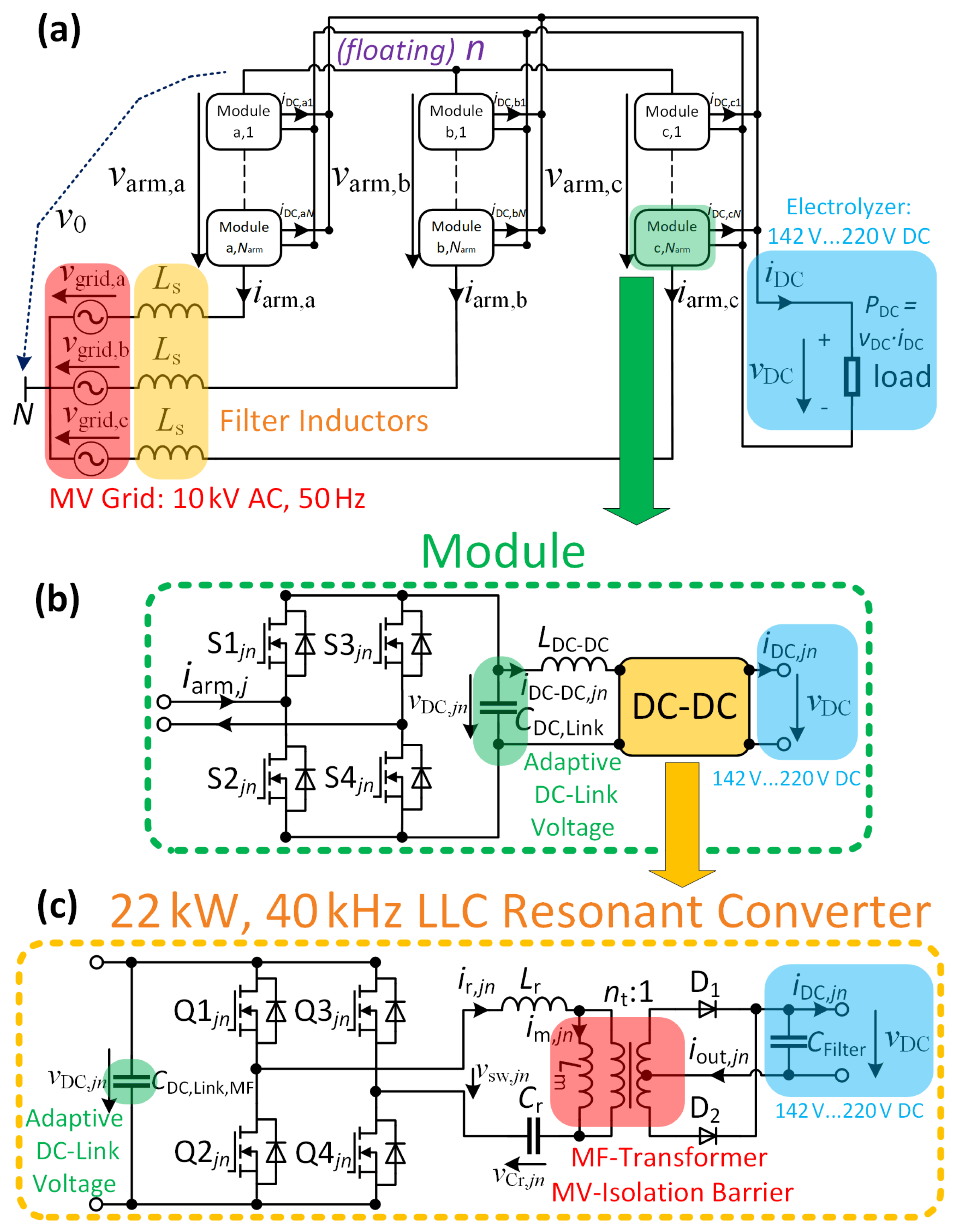
3. Design of the 22 kW LLC Resonant Converter

After the maximum power of an individual LLC has been set at P ^ L L C = 22.2   k W , the components for the inverter, transformer and rectifier are specified. The leakage inductance of the integrated transformer provides the required resonance inductance   L r .

3.1. Components of the SiC Inverter and Rectifier Stage

Two C3M0075120K SiC MOSFETs are paralleled for Q 1 to Q 4 to meet the expected resonant current rating of I r , j n = 35   A at full load. The power density of the forced air-cooled inverter stage is 19.6   k W / d m 3 .
Each rectifier SiC Schottky diode C5D50065D can withstand a voltage of 650 V. This is sufficient since the maximum voltage across a diode is 2 · v ^ D C = 440   V (center tapped transformer). Four diodes are paralleled for D 1 and four for D 2 to reduce the thermal load of each diode. The power density of the forced air-cooled rectifier stage is 19.5   k W / d m 3 .
Printed circuit boards (PCBs) are used for both the inverter and the rectifier stage, which are shown in Figure 4b,c. Furthermore, the custom-designed circuit board of the digital controller based on TI C2000, TMS320F28027, is shown in Figure 4a.

3.2. Components of the Resonant Tank

The medium frequency transformer (MFT) must transfer the power of 22.2   k W and withstand the grid voltage of 10   k V [20]. Only a few cores with a sufficiently large winding window are available to include the windings and the insulation material. Two parallel EPCOS N87 U93/76/30 cores with a center-tapped bifilar winding on the secondary side are constructed to halve the number of diodes and losses of the rectifier [21]. A litz wire of 2160 · 0.071   m m is utilized for the primary side of the transformer, and the full-load RMS current density is approximately 4.1 A m m 2 .
The leakage inductance of the transformer is relatively large due to the large distance between the primary and secondary windings to provide the required galvanic isolation. As a positive side effect, it provides the required resonance inductance L r [22]. The values for the parameters of the resonant circuit are identical to the converter in [11] and are summarized in Table 1. The parameters are selected in such a way that zero-voltage switching (ZVS) is achieved for all points of operation [11]. A constant dead time of 200   n s is used for all points of operation to simplify inverter control.

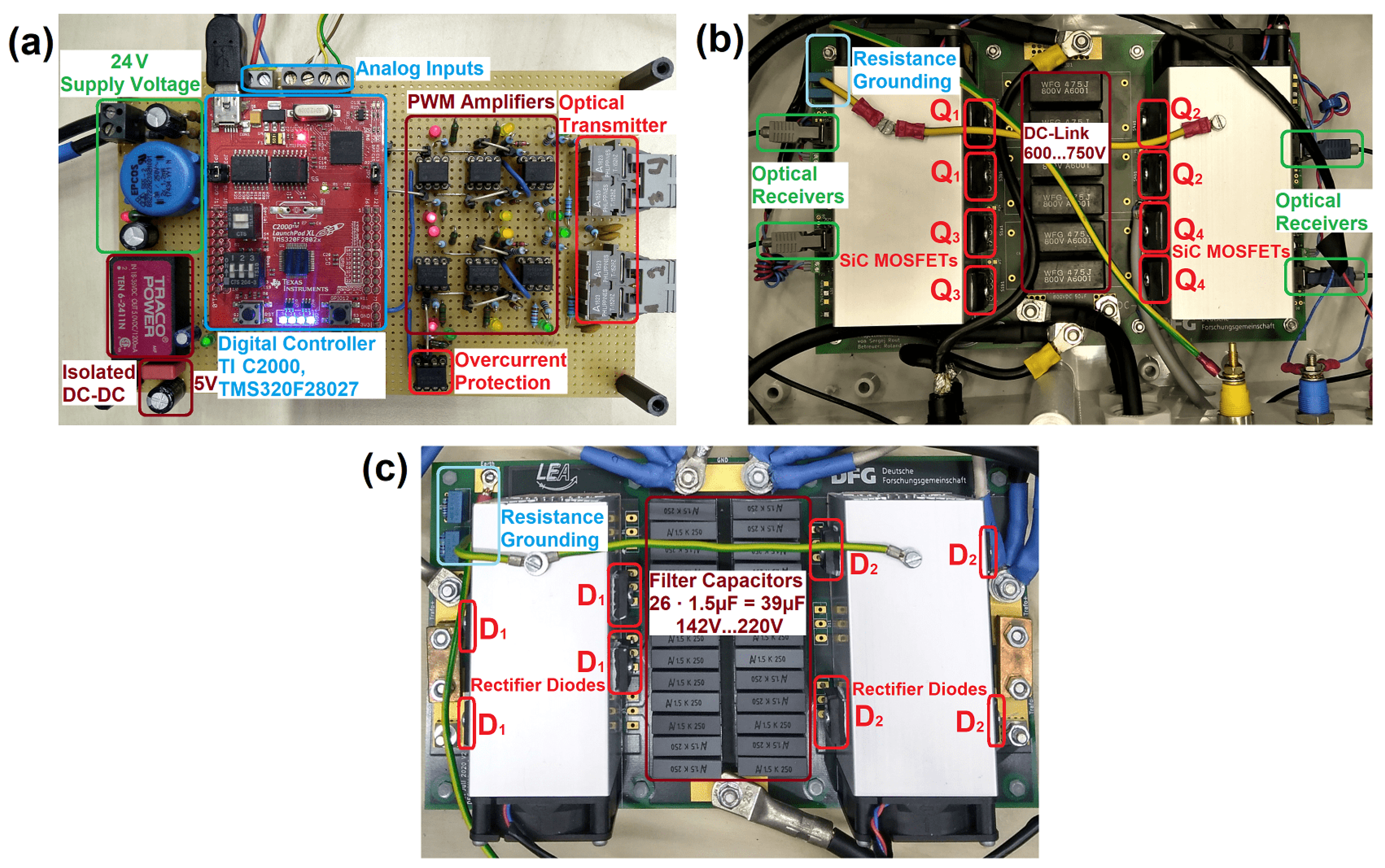
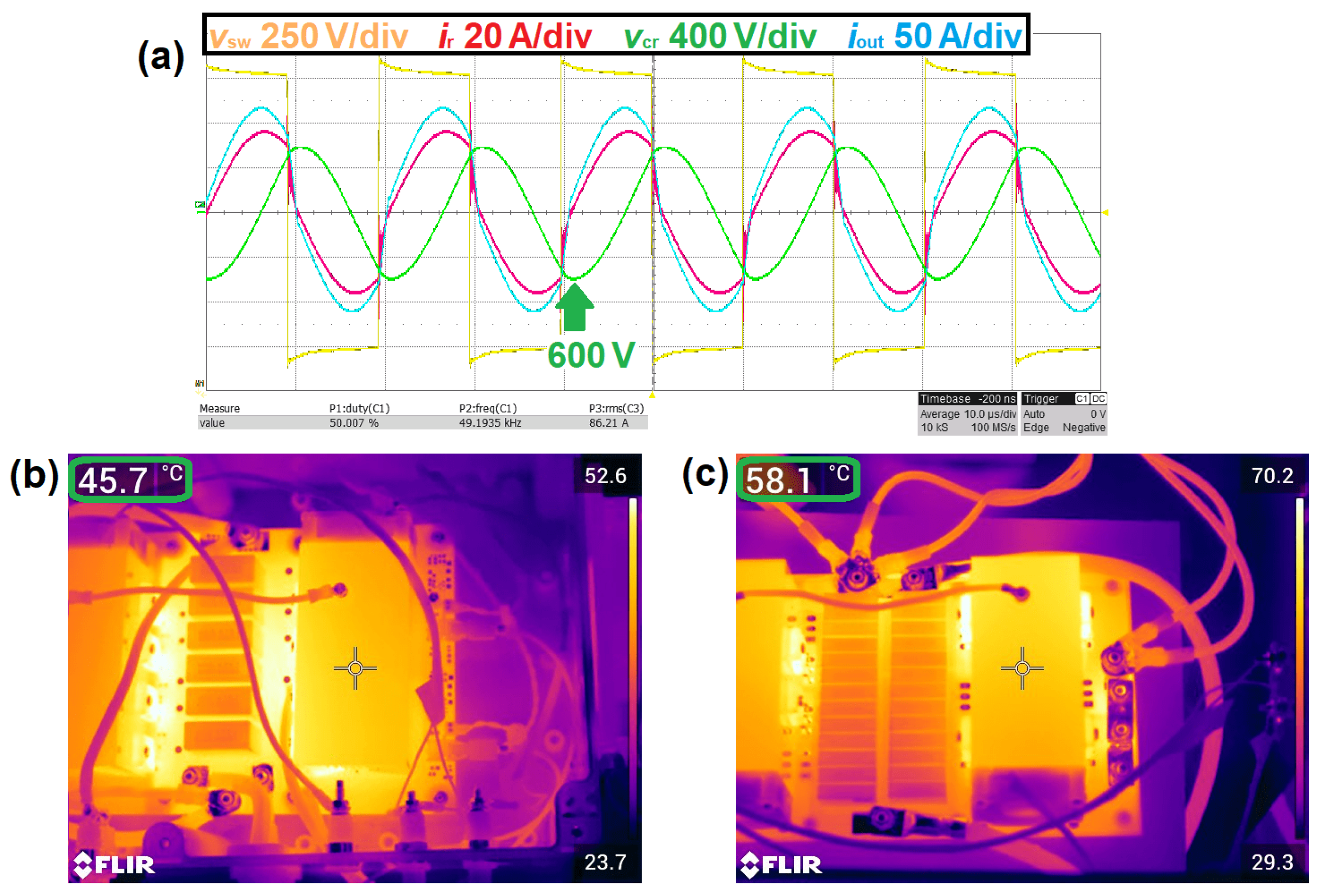
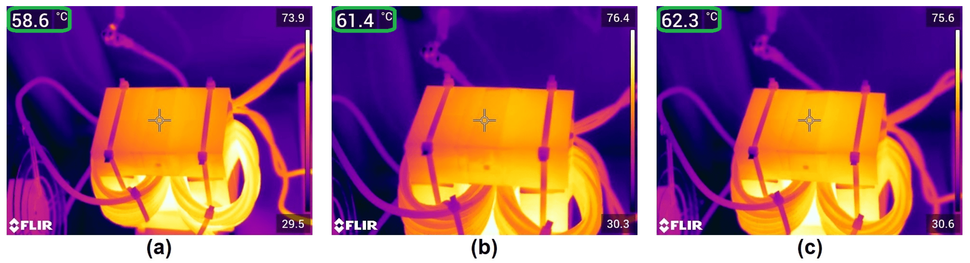
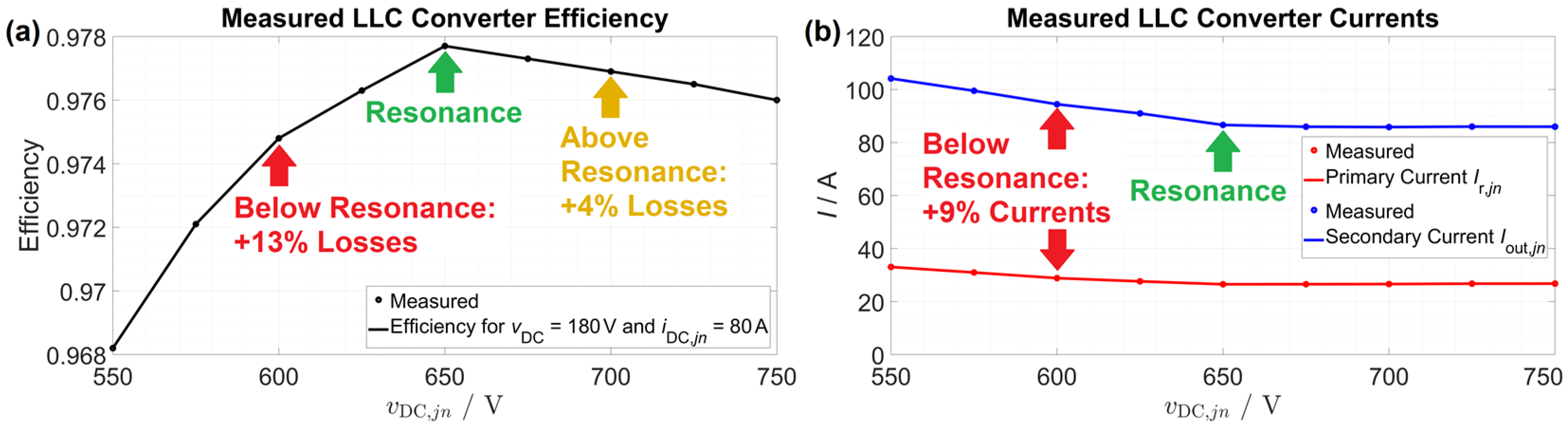
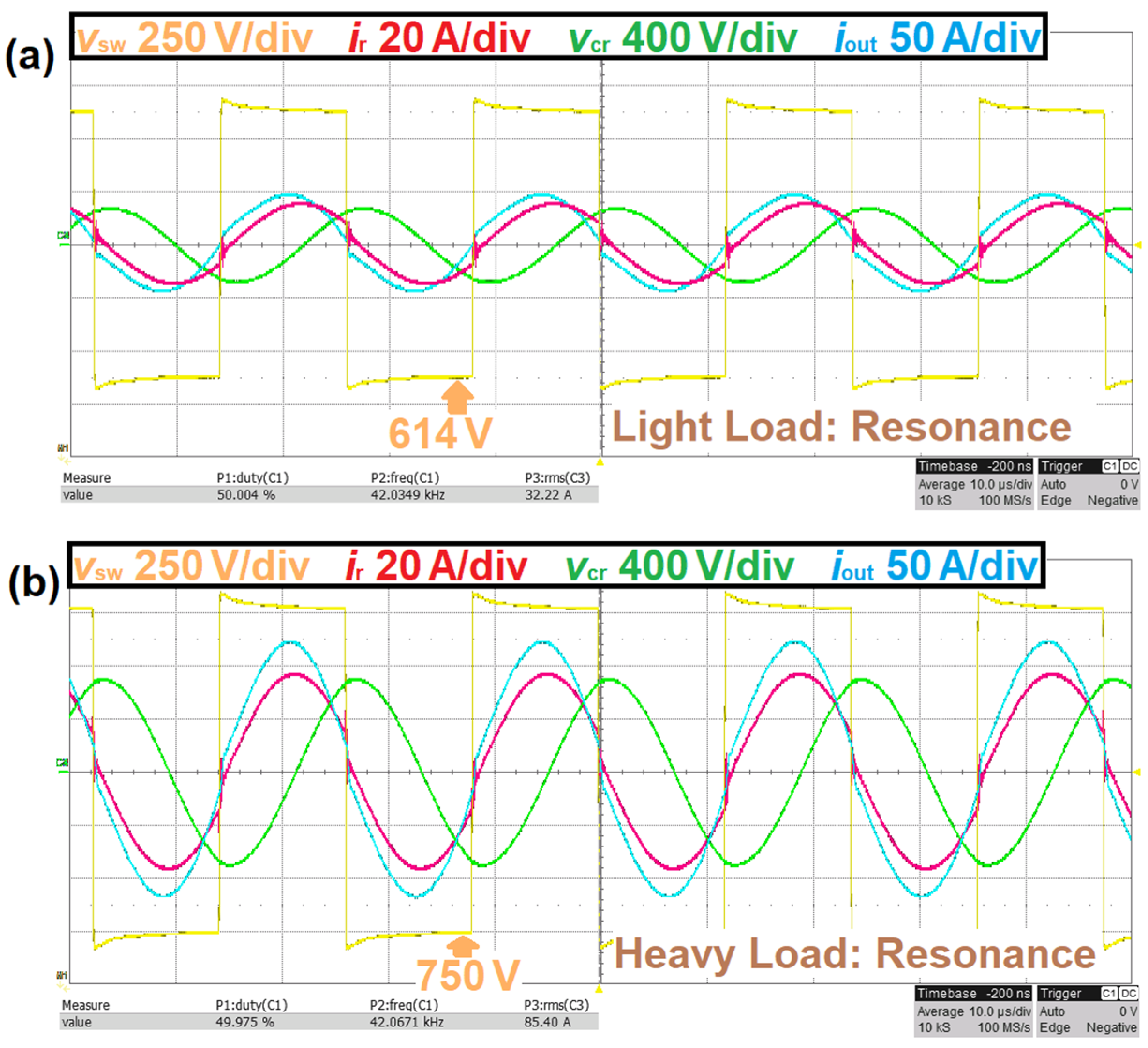
4. Experimental Results

The DC-link voltage applied to the LLC resonant converter can be controlled during operation to maximize the efficiency. This section will show that resonant operation is the most efficient operation and that below-resonance operation results in the highest losses.
First, the DC-link voltage is set to a very low voltage of v D C , j n = 550   V . The resulting oscilloscope recordings for the average operating point of v D C = 180   V and i D C , j n = 80   A are shown in Figure 5a. The LLC converter operates well below resonance with f s , 550   V = 0.73 f 0 = 29.15   k H z . As expected, the secondary current is i o u t t s w i t c h = 0   A during the switching event. The DC-link voltage v D C , j n and DC input current i D C , D C , j n are measured with calibrated equipment and are used to calculate the total LLC input power. The measured secondary output voltage v D C and current i D C , j n are used to calculate the output power. To ensure steady-state temperatures, the efficiency is recorded after 10 min of operation for this and other operating points. The overall measured efficiency is only η 550   V = 96.8 % for a lower input voltage of v D C , j n = 550   V . Additionally, the peak resonant capacitor voltage has a high value of v ^ C r , 550   V = 1160   V . This also results in high resonant capacitor losses. However, zero-voltage switching (ZVS) is still achieved for this operating point because a positive primary current of i r t s w i t c h 8   A is switched. This is sufficient to fully discharge the transistors’ parasitic output capacitances within 200   n s .
Now, the DC-link voltage is increased to v D C , j n = 650   V , and the resulting oscilloscope recordings are shown in Figure 6a for the same load of v D C = 180   V and i D C , j n = 80   A . Now, the LLC converter operates nearly at resonance with f s , 650   V = 1.03 f 0 = 41.42   k H z , and the primary and secondary currents are close to the sinusoidal shape. The LLC efficiency increases by 1.0 % to η 650   V = 97.8 % due to the reduced primary and secondary currents. The transformer skin effect and proximity losses are also reduced due to the sinusoidal shape of the currents. The increased efficiency is also clearly visible with a thermal camera. The inverter heat sink temperature is reduced from 49.7 °C to 43.0 °C, as shown by comparing Figure 5b and Figure 6b. Figure 6c shows the rectifier heatsink temperature of 57.6 °C for a DC-link voltage of v D C , j n = 650   V .
Additionally, the peak resonant capacitor voltage is reduced from v ^ C r , 550   V = 1160   V to v ^ C r , 650   V = 710   V by 39 % . Here, the switched primary transformer current is slightly lagging behind the secondary current. As a result, the positive primary current i r t s w i t c h 13   A leads to ZVS.
It is possible to operate the LLC converter above resonance by increasing the DC-link voltage to v D C , j n = 750   V , and the resulting oscilloscope recordings and thermal images are shown in Figure 7. The converter’s efficiency is η 750   V = 97.6 % , and this is only 0.2 % lower than at resonance with v D C , j n = 650   V . This is confirmed by the thermal images in Figure 7b,c. The inverter and rectifier steady-state temperatures are slightly higher than in Figure 6b,c. Now, the peak resonant capacitor voltage is v ^ C r , 750   V = 600   V . The switched primary current i r t s w i t c h 29   A is higher than for v D C , j n = 550   V and v D C , j n = 650   V . This results in larger switching losses and is one reason for the slight efficiency reduction. However, ZVS is still achieved. Selecting a dead time below 200   n s would likely reduce the switching losses, but a dynamic dead time is out of the scope of this article. ZVS is achieved for all points of operation.
Interestingly, the transformer core temperature and thus the core losses are nearly independent of the input DC-link voltage v D C , j n , as shown in the thermal images in Figure 8. The frequency for v D C , j n = 750   V is f s , 750   V = 49.19   k H z and only f s , 550   V = 29.15   k H z for v D C , j n = 550   V . However, the calculated peak magnetic flux density is B ^ 550   V = 214   m T for v D C , j n = 550   V and only B ^ 750   V = 162   m T for v D C , j n = 750   V . So, the loss increase due to the higher frequency is compensated by a reduced peak flux density.
Additional measurements are performed for the DC-link voltages v D C , j n = 550   V 750   V in steps of 25   V . The measured efficiencies are shown in Figure 9a. Also, the measured RMS values of the primary and secondary currents are diagrammed in Figure 9b. All measurements are performed at thermal steady-state after 10 min of operation.
The experimental results clearly show that the resonant operation achieves the highest efficiency, and a deviation of the DC-link voltage from the optimal value adds additional losses. However, the losses increase significantly below resonance. This is mainly caused by increased primary and secondary transformer RMS currents.

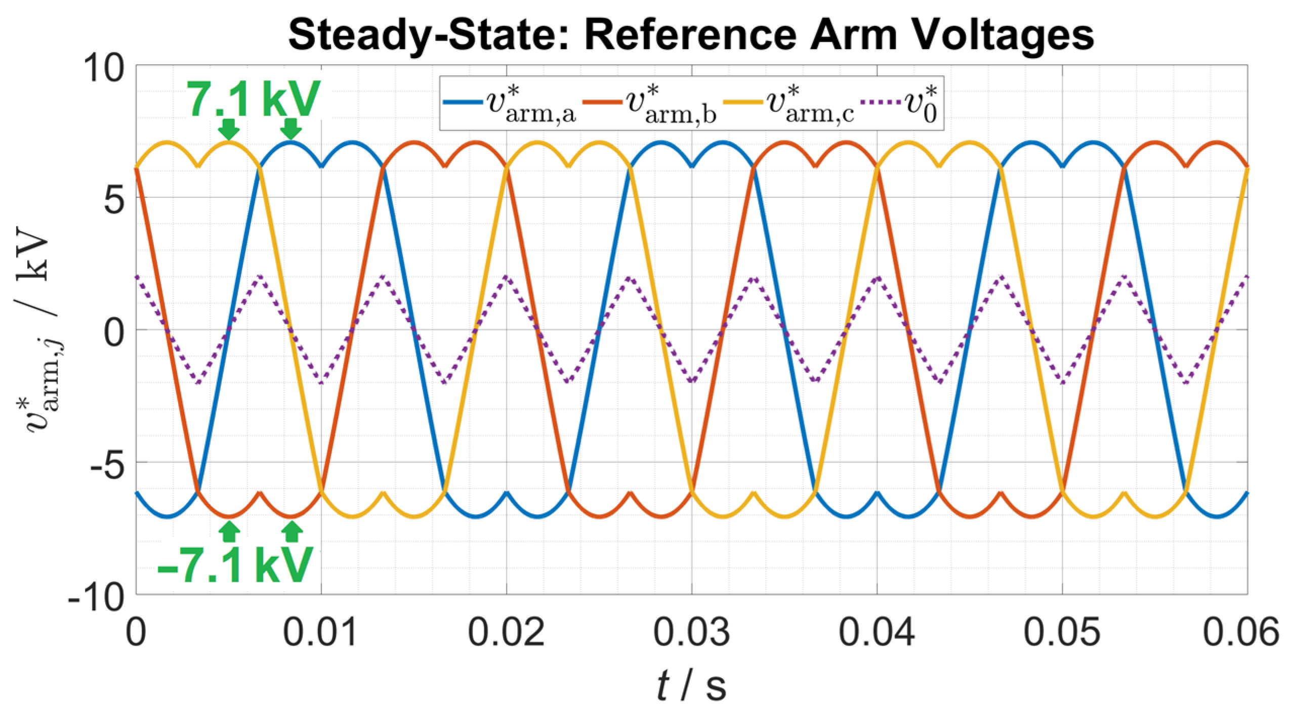
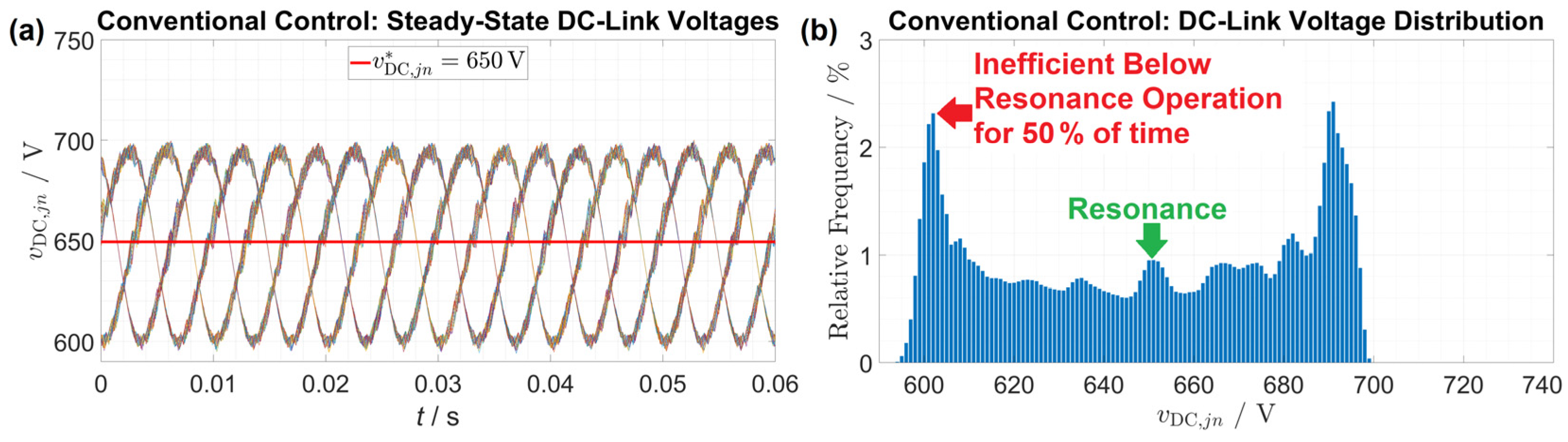
Conventional Method to Determine DC-Link Voltage

The experimental results clearly show that resonant operation is more efficient than below- or above-resonance operation. This is also confirmed by many publications [23,24,25,26,27,28,29,30,31,32,33,34,35] where resonance is achieved by controlling the input voltage of the LLC converter. Figure 10a shows resonant operation for an output voltage of v D C = 171   V and an input voltage v D C , j n = 614   V . A higher output voltage of v D C = 206   V requires a higher input voltage of v D C , j n = 750   V to achieve resonance, as shown in Figure 10b.
The ratio between the input and output voltage of the LLC converter is nearly constant at resonance [23,24,25,26,27,28,29,30,31,32,33,34,35] and is slightly higher than the transformer transfer ratio n t = 3.44 due to converter losses. By accounting for the losses, the input voltage v D C , j n should be approximately 3.6 times higher than the measured output voltage v D C to achieve resonance for this investigated LLC converter. This can be expressed by the following control equation for this specific LLC resonant converter:
v D C , j n = m i n ( m a x ( 3.6 · v D C , 600   V ) , 750   V )
If the LLC input voltage is constant and does not show a low-frequency ripple, then Equation (1) guarantees the highest efficiency. As shown in Section 2, the resulting reference DC-link voltage v D C , j n must remain between the defined boundaries of 600   V and 750   V . The next section will show that the low-frequency DC-link voltage ripple causes the LLC converter to operate below and above resonance at a lower efficiency.

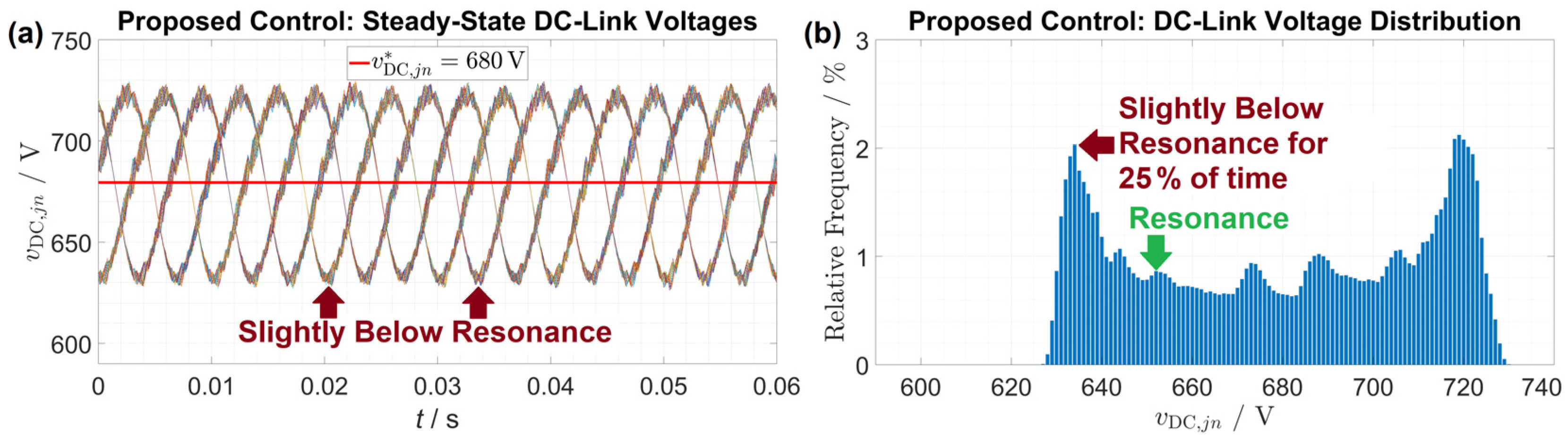
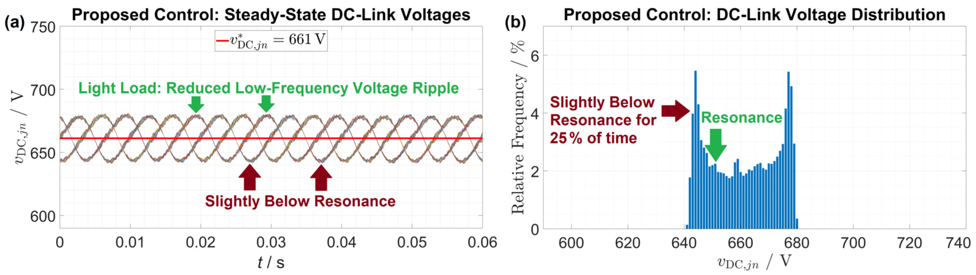
5. Simulation Results

The experimental results demonstrate that the converter operates with the highest efficiency of η 650   V = 97.8 % at resonance with a DC-link voltage of v D C , j n = 650   V for the operating point v D C = 180   V and i D C , j n = 80   A . However, the DC-link capacitor shows a low-frequency peak-to-peak voltage ripple of 100   V due to a pulsating input power [36] and a relatively small DC-link capacitor with C D C , L i n k = 600   µ F . Often, the LLC converter operates below resonance with v D C , j n = 600   V or above resonance with v D C , j n = 700   V , as shown in Figure 11. The additional losses decrease the average efficiency to approximately η ¯ 650   V = 97.66 % . Selecting a larger DC-link capacitance C D C , L i n k would decrease the peak-to-peak voltage ripple and increase efficiency, but this would add additional costs. Better balancing within each phase [37,38,39,40,41] will not significantly improve the overall efficiency since the DC-link voltage in each phase deviates only a few volts from each other. Reducing the LLC output power for lower instantaneous DC-link voltages and increasing the LLC power for higher DC-link voltages increase the efficiency [11], but this is out of the scope of this work.
The average efficiency can be improved for free by increasing the reference DC-link voltage from v D C , j n = 650   V to v D C , j n = 680   V . The resulting steady-state DC-link voltages are shown in Figure 12a. Now, the LLC converter operates mostly above resonance and only for a brief time slightly below resonance. The overall efficiency increases to η ¯ 680   V = 97.70 % and the losses decrease by 2 % . A further increase of v D C , j n would reduce the overall efficiency because over-resonant operation also causes additional losses. Operating the LLC always above resonance with v D C , j n = 700   V would result in a slightly decreased efficiency of η ¯ 700   V = 97.69 %   ( 0.01 % ) .
Now, the DC-link voltage lies within v D C , j n = 630   V 730   V The efficiency for the LLC input voltage v D C , j n = 630   V corresponds roughly to the efficiency at v D C , j n = 730   V , as can be seen in Figure 9a. Finally, the measured peak resonant capacitor voltage decreases from v ^ C r , 600   V = 910   V to approximately v ^ C r , 630   V = 790   V (− 13 % ).

Proposed Method to Determine DC-Link Voltage

According to the proposed method, the efficiency of the LLC converter has to be measured for different DC-link voltages for one operating point. Then, the average efficiency is calculated for a whole grid period for different nominal DC-link voltages. For the closely investigated point of operation with v D C = 180   V and i D C , j n = 80   A , the optimal reference DC-link voltage is determined numerically with v D C , j n = 680   V . The LLC converter operates approximately 75% of the time over resonance and only 25% of the time below resonance. It is expected that the over resonance efficiency is generally higher due to smaller RMS values of transformer currents. The authors propose to select the reference DC-link voltage in such a way that the LLC converter operates approximately 75% of the time over resonance and only 25% of the time below resonance within a grid period. In contrast, the conventional method with Equation (1) operates the LLC converter below resonance 50% of the time.
Figure 13 shows the steady-state DC-link voltages at light load with v D C = 180   V and i D C , j n = 30   A . Here, the optimal DC-link voltage is v D C , j n = 661   V to achieve below-resonance operation for approximately 25% of the time and maximize the overall efficiency.
For an output current of i D C , j n = 80   A , the DC-link reference voltage v D C , j n has to be increased by 30   V to maximize efficiency, as shown in Figure 12. An output current of only i D C , j n = 30   A requires a 11   V DC-link voltage increase, as shown in Figure 13. Other operating points were tested, and the optimal DC-link voltage increase is roughly proportional to the output current i D C , j n . The conventional Equation (1) for calculation of the reference DC-link voltage is adapted to account for the low-frequency voltage ripple:
v D C , j n = m i n ( m a x ( 3.6 · v D C + 30   V · i D C , j n 80   A ,   600   V ) , 750   V )
Using Equation (2) results in steady-state voltages, as shown in Figure 12 and Figure 13. This minimizes the additional losses caused by below and above-resonance operation. Of course, Equation (2) has to be adapted to each specific LLC converter, and the given parameters of Equation (2) are only valid for the converter as specified in Table 1. Table 2 summarizes the advantages of the proposed DC-link voltage control method. The efficiency is increased and the peak resonant capacitor voltage v ^ C r is reduced by 13%.
Additionally, the transistors S1 to S4 in the AC-DC stage of the CHB, shown in Figure 1b, also cause switching losses, which are voltage-dependent. Future work should refine Equation (2) to also consider the switching losses of the AC-DC stage. It is likely that a slightly lower DC-link voltage v D C , j n can increase the system’s overall efficiency by reducing these switching losses.

6. Conclusions

This paper presents an efficiency optimization of a 22.2 kW LLC resonant converter for a single module of a 1 MW cascaded H-bridge (CHB) converter powering a hydrogen electrolyzer. Conventionally, the module DC-link voltage is controlled to operate the LLC converter at resonance. However, the DC-link voltage shows a peak-to-peak voltage ripple of 100 V in this cascaded H-bridge converter. This forces the current controller to adapt the switching frequency of the LLC converter within the grid period to ensure constant power transfer. As a result, the LLC converter operates 50% of the time below resonance and 50% of the time above resonance. Both operations increase the overall losses. However, detailed measurements of a 22 kW LLC converter show a significant increase in losses below resonance. This is confirmed by thermal images of the inverter and rectifier. In contrast, operation above resonance increases the losses only slightly. As a result, it is more efficient to increase the reference DC-link voltage from 650 V to 680 V to mostly avoid below-resonance operation. Now, the converter operates only 25% of the time below resonance. This increases the average converter efficiency from 97.66% to 97.70% with identical hardware. This corresponds to a 2% loss reduction. At the same time, the peak value of the resonant capacitor voltage decreases by 13%. Finally, a new equation is proposed to calculate the reference DC-link voltage for all operating points and maximize the LLC converter efficiency. It is expected that the proposed method can also increase the efficiency for many different single-phase grid-connected inverters.

Author Contributions

Conceptualization, R.U.; methodology, R.U.; software, R.U.; validation, R.U.; formal analysis, R.U.; investigation, R.U.; resources, F.S.; data curation, R.U.; writing—original draft preparation, R.U.; writing—review and editing, F.S. and J.B.; visualization, R.U.; supervision, F.S.; project administration, F.S.; funding acquisition, F.S. All authors have read and agreed to the published version of the manuscript.

Funding

The authors would like to thank the German Research Foundation (DFG) for funding this research under the project number 456097802.

Data Availability Statement

Data is contained within the article.

Conflicts of Interest

The authors declare no conflicts of interest.

References

  1. Chandesris, M.; Médeau, V.; Guillet, N.; Chelghoum, S.; Thoby, D.; Fouda-Onana, F. Membrane degradation in PEM water electrolyzer: Numerical modeling and experimental evidence of the influence of temperature and current density. Int. J. Hydrogen Energy 2015, 40, 1353–1366. [Google Scholar] [CrossRef]
  2. Vargas-Ferrer, P.; Álvarez-Miranda, E.; Tenreiro, C.; Jalil-Vega, F. Integration of high levels of electrolytic hydrogen production: Impact on power systems planning. J. Clean. Prod. 2023, 409, 137110. [Google Scholar] [CrossRef]
  3. Yodwong, B.; Guilbert, D.; Phattanasak, M.; Kaewmanee, W.; Hinaje, M.; Vitale, G. AC-DC Converters for Electrolyzer Applications: State of the Art and Future Challenges. Electronics 2020, 9, 912. [Google Scholar] [CrossRef]
  4. Solanki, J. High Power Factor High-Current Variable-Voltage Rectifiers. Ph.D. Thesis, Paderborn University, Paderborn, Germany, 2015. [Google Scholar]
  5. Chen, M.; Chou, S.-F.; Blaabjerg, F.; Davari, P. Overview of Power Electronic Converter Topologies Enabling Large-Scale Hydrogen Production via Water Electrolysis. Appl. Sci. 2022, 12, 1906. [Google Scholar] [CrossRef]
  6. Rothmund, D.; Guillod, T.; Bortis, D.; Kolar, J.W. 99% Efficient 10 kV SiC-Based 7 kV/400 V DC Transformer for Future Data Centers. IEEE J. Emerg. Sel. Top. Power Electron. 2019, 7, 753–767. [Google Scholar] [CrossRef]
  7. Li, Z.; Hsieh, Y.-H.; Li, Q.; Lee, F.C.; Ahmed, M.H. High-Frequency Transformer Design with High-Voltage Insulation for Modular Power Conversion from Medium-Voltage AC to 400-V DC. In Proceedings of the 2020 IEEE Energy Conversion Congress and Exposition (ECCE), Detroit, MI, USA, 11–15 October 2020; pp. 5053–5060. [Google Scholar]
  8. Aghoy, A.R.; Ebrahimi, J.; Pahlevani, M.; Bakhshai, A. Feasibility Review of Multilevel Converters in Electric Vehicle Chargers. In Proceedings of the 2024 IEEE Canadian Conf. on Electrical and Computer Engineering (CCECE), Kingston, ON, Canada, 6–9 August 2024; pp. 495–500. [Google Scholar]
  9. Koponen, J.; Ruuskanen, V.; Kosonen, A.; Niemelä, M.; Ahola, J. Effect of Converter Topology on the Specific Energy Consumption of Alkaline Water Electrolyzers. IEEE Trans. Power Electron. 2019, 34, 6171–6182. [Google Scholar] [CrossRef]
  10. Ruuskanen, V.; Koponen, J.; Kosonen, A.; Niemelä, M.; Ahola, J.; Hämäläinen, A. Power quality and reactive power of water electrolyzers supplied with thyristor converters. J. Power Sources 2020, 459, 228075. [Google Scholar] [CrossRef]
  11. Unruh, R.; Böcker, J.; Schafmeister, F. Experimentally Verified 22 kW, 40 kHz LLC Resonant Converter Design with new Control for a 1 MW Cascaded H-Bridge Converter. In Proceedings of the 2024 Energy Conversion Congress & Expo Europe (ECCE Europe), Darmstadt, Germany, 2–6 September 2024. [Google Scholar]
  12. Kurokawa, F.; Murata, K. A new fast digital P-I-D control LLC resonant converter. In Proceedings of the 2011 International Conference on Electrical Machines and Systems, Beijing, China, 20–23 August 2011. [Google Scholar]
  13. Kim, J.; Kim, C.; Kim, J.; Lee, J.; Moon, G. Analysis on Load-Adaptive Phase-Shift Control for High Efficiency Full-Bridge LLC Resonant Converter Under Light-Load Conditions. IEEE Trans. Pow. Electr. 2016, 31, 4942–4955. [Google Scholar] [CrossRef]
  14. Lumbreras, D.; Gálvez, E.; Collado, A.; Zaragoza, J. Trends in Power Quality, Harmonic Mitigation and Standards for Light and Heavy Industries: A Review. Energies 2020, 13, 5792. [Google Scholar] [CrossRef]
  15. Lu, B.; Liu, W.; Liang, Y.; Lee, F.C.; van Wyk, J.D. Optimal design methodology for LLC resonant converter. In Proceedings of the 21th Annual IEEE Applied Power Electronics Conference and Exposition, APEC ’06, Dallas, TX, USA, 19–23 March 2006. [Google Scholar]
  16. Rivera, S.; Wu, B.; Kouro, S.; Wang, H.; Zhang, D. Cascaded H-bridge multilevel converter topology and three-phase balance control for large scale photovoltaic systems. In Proceedings of the 2012 3rd IEEE International Symposium on Power Electronics for Distributed Generation Systems (PEDG), Aalborg, Denmark, 25–28 June 2012. [Google Scholar]
  17. Unruh, R.; Schafmeister, F.; Böcker, J. Zero-Sequence Voltage Reduces DC-Link Capacitor Demand in Cascaded H-Bridge Converters for Large-Scale Electrolyzers by 40%. In Proceedings of the 2022 24th European Conference on Power Electronics and Applications (EPE’22 ECCE Europe), Hanover, Germany, 5–9 September 2022. [Google Scholar]
  18. Langbauer, T.; Menzi, D.; Marugg, V.; Vollmaier, F.; Azurza, J.; Kasper, M.; Kolar, J.W. Third-Harmonic-Type Modulation Minimizing the DC-Link Energy Storage Requirement of Isolated Phase-Modular Three-Phase PFC Rectifier Systems. IEEE Access 2023, 11, 34359–34371. [Google Scholar] [CrossRef]
  19. Xie, D.; Lin, C.; Zhang, Y.; Sangwongwanich, A.; Ge, X.; Feng, X.; Wang, H. Diagnosis and Resilient Control for Multiple Sensor Faults in Cascaded H-Bridge Multilevel Converters. IEEE Trans. Power Electron. 2023, 38, 11435–11450. [Google Scholar] [CrossRef]
  20. Mogorovic, M.; Dujic, D. 100 kW, 10 kHz Medium-Frequency Transformer Design Optimization and Experimental Verification. IEEE Trans. Power Electron. 2019, 34, 1696–1708. [Google Scholar] [CrossRef]
  21. Jung, J. Bifilar Winding of a Center-Tapped Transformer Including Integrated Resonant Inductance for LLC Resonant Converters. IEEE Trans. Power Electron. 2013, 28, 615–620. [Google Scholar] [CrossRef]
  22. Choi, H. Analysis and Design of LLC Resonant Converter with Integrated Transformer. In Proceedings of the APEC 07—22th Annual IEEE Applied Power Electronics Conference and Exposition, Anaheim, CA, USA, 25 February–1 March 2007; pp. 1630–1635. [Google Scholar]
  23. Kim, B.-C.; Park, K.-B.; Kim, C.-E.; Lee, B.-H.; Moon, G.-W. LLC Resonant Converter with Adaptive Link-Voltage Variation for a High-Power-Density Adapter. IEEE Trans. Power Electron. 2010, 25, 2248–2252. [Google Scholar] [CrossRef]
  24. Su, Z.-J.; Lai, Y.-S. On-line DC-link voltage control of LLC resonant converter for server power applications. In Proceedings of the 2014 IEEE Energy Conversion Congress and Exposition (ECCE), Pittsburgh, PA, USA, 14–18 September 2014. [Google Scholar]
  25. Wang, H.; Dusmez, S.; Khaligh, A. Maximum Efficiency Point Tracking Technique for LLC-Based PEV Chargers Through Variable DC Link Control. IEEE Trans. Ind. Electron. 2014, 61, 6041–6049. [Google Scholar] [CrossRef]
  26. Wang, X.; Jiang, C.; Lei, B.; Teng, H.; Bai, H.K.; Kirtley, J.L. Power-Loss Analysis and Efficiency Maximization of a Silicon-Carbide MOSFET-Based Three-Phase 10-kW Bidirectional EV Charger Using Variable-DC-Bus Control. IEEE J. Emerg. Sel. Top. Power Electron. 2016, 4, 880–892. [Google Scholar] [CrossRef]
  27. Liu, Z.; Li, B.; Lee, F.C.; Li, Q. High-Efficiency High-Density Critical Mode Rectifier/Inverter for WBG-Device-Based On-Board Charger. IEEE Trans. Ind. Electron. 2017, 64, 9114–9123. [Google Scholar] [CrossRef]
  28. Shih, L.-C.; Liu, Y.-H.; Luo, Y.-F. Adaptive DC-link voltage control of LLC resonant converter. CPSS Trans. Power Electron. Appl. 2018, 3, 187–196. [Google Scholar] [CrossRef]
  29. Li, B.; Li, Q.; Lee, F.C.; Liu, Z.; Yang, Y. A High-Efficiency High-Density Wide-Bandgap Device-Based Bidirectional On-Board Charger. IEEE J. Emerg. Sel. Top. Power Electron. 2018, 6, 1627–1636. [Google Scholar] [CrossRef]
  30. Lai, Y.-S.; Yu, M.-H. Online Autotuning Technique of Switching Frequency for Resonant Converter Considering Resonant Components Tolerance and Variation. IEEE J. Emerg. Sel. Top. Power Electron. 2018, 6, 2315–2324. [Google Scholar] [CrossRef]
  31. Pandey, R.; Singh, B. PFC-SEPIC converter-fed half-bridge LLC resonant converter for e-bike charging applications. IET Electr. Syst. Transp. 2020, 10, 225–233. [Google Scholar] [CrossRef]
  32. Li, H.; Zhang, Z.; Wang, S.; Tang, J.; Ren, X.; Chen, Q. A 300-kHz 6.6-kW SiC Bidirectional LLC Onboard Charger. IEEE Trans. Ind. Electron. 2020, 67, 1435–1445. [Google Scholar] [CrossRef]
  33. Unruh, R.; Schafmeister, F.; Böcker, J. 11kW, 70kHz LLC Converter Design with Adaptive Input Voltage for 98% Efficiency in an MMC. In Proceedings of the 2020 IEEE 21st Workshop on Control and Modeling for Power Electronics (COMPEL), Aalborg, Denmark, 9–12 November 2020. [Google Scholar]
  34. Yu, G.; Choi, S. An Effective Integration of APM and OBC with Simultaneous Operation and Entire ZVS Range for Electric Vehicle. IEEE Trans. Power Electron. 2021, 36, 10343–10354. [Google Scholar] [CrossRef]
  35. Zhao, S.; Kempitiya, A.; Chou, W.T.; Palija, V.; Bonfiglio, C. Variable DC-Link Voltage LLC Resonant DC/DC Converter with Wide Bandgap Power Devices. IEEE Trans. Ind. Appl. 2022, 58, 2965–2977. [Google Scholar] [CrossRef]
  36. Unruh, R.; Böcker, J.; Schafmeister, F. An Optimized Third-Harmonic Injection Reduces DC-Link Voltage Ripple in Cascaded H-Bridge Converters up to 50% for all Power Factors. In Proceedings of the 2023 25th European Conference on Power Electronics and Applications (EPE’23 ECCE Europe), Aalborg, Denmark, 4–8 September 2023. [Google Scholar]
  37. Moosavi, M.; Farivar, G.; Iman-Eini, H.; Shekarabi, S.M. A voltage balancing strategy with extended operating region for cascaded H-bridge converters. IEEE Trans. Power Electron. 2014, 29, 5044–5053. [Google Scholar] [CrossRef]
  38. Miranbeigi, M.; Iman-Eini, H. Hybrid Modulation Technique for Grid-Connected Cascaded Photovoltaic Systems. IEEE Trans. Ind. Electron. 2016, 63, 7843–7853. [Google Scholar] [CrossRef]
  39. Wang, S.; Jiao, N.; Ma, J.; Liu, T.; Liu, X. Analysis and Optimization of Voltage Balancing Control Limits for Cascaded H-Bridge Rectifiers. IEEE Trans. Ind. Electron. 2021, 68, 10677–10687. [Google Scholar] [CrossRef]
  40. Ko, Y.; Tcai, A.; Liserre, M. DC-Link Voltage Balancing Modulation for Cascaded H-Bridge Converters. IEEE Access 2021, 9, 103524–103532. [Google Scholar] [CrossRef]
  41. Li, J.; Chen, J.; Gong, C.; He, Q. Improved Square Wave Injection Strategy for the Voltage Balance Control of Cascaded H-Bridge Rectifier. IEEE Trans. Transp. Electrif. 2023, 9, 3711–3722. [Google Scholar] [CrossRef]
Figure 1. (a) Three-phase cascaded H-bridge converter, (b) module structure, (c) LLC resonant converter of each module. DC-link voltage v D C , j n can be adjusted for more efficient operation.
Electronics 14 01517 g001
Figure 2. Operating area of a 1 MW electrolyzer. The LLC input voltage can be adjusted between v D C , j n = 600   V and v D C , j n = 750   V to operate the LLC converter closer to resonance.
Electronics 14 01517 g002
Figure 3. Steady-state reference arm voltages are calculated with the method published in [16,17,18].
Electronics 14 01517 g003
Figure 4. (a) DSP-based digital controller used for calculating the switching frequency f s . The signals are transferred via fiber optic to the (b) inverter stage gate drivers to switch the transistors Q1 to Q4. (c) shows the diodes D1 and D2 of the passive rectifier.
Electronics 14 01517 g004
Figure 5. (a) Oscilloscope recordings with v D C , j n = 550   V , v D C = 180   V and i D C , j n = 80   A result in below-resonance operation with f s , 550   V = 0.73 f 0 = 29.15   k H z . The inverter heatsink (b) shows a high temperature of 49.7 °C, and the rectifier (c) shows a temperature of 63.6 °C due to the high losses. The temperatures are measured at the center of the image at the cross symbol.
Electronics 14 01517 g005
Figure 6. (a) Oscilloscope recordings with v D C , j n = 650   V , v D C = 180   V and i D C , j n = 80   A result in nearly resonance operation with f s , 650   V = 1.03 f 0 = 41.42   k H z . The inverter heatsink (b) shows a low temperature of 43.0 °C, and the rectifier heatsink (c) shows a temperature of 57.6 °C. The temperatures are measured at the center of the image at the cross symbol.
Electronics 14 01517 g006
Figure 7. (a) Oscilloscope recordings with v D C , j n = 750   V , v D C = 180   V and i D C , j n = 80   A result in over-resonant operation with f s , 750   V = 1.23 f 0 = 49.19   k H z . The inverter heatsink (b) shows a temperature of 45.7 °C, and the rectifier heatsink (c) shows a temperature of 58.1 °C. The temperatures are measured at the center of the image at the cross symbol.
Electronics 14 01517 g007
Figure 8. (a) Transformer core temperature is 58.6 °C for v D C , j n = 550   V , (b) 61.4 °C for v D C , j n = 650   V and (c) 62.3 °C for v D C , j n = 750   V . The core losses are nearly independent of the DC-link voltage. The temperatures are measured at the center of the image at the cross symbol.
Electronics 14 01517 g008
Figure 9. (a) Efficiency at thermal steady-state for different DC-link voltages. (b) RMS values of primary and secondary currents. Below-resonant operation is not efficient due to the high currents.
Electronics 14 01517 g009
Figure 10. (a) Oscilloscope recordings for light load with v D C = 171   V and i D C , j n = 30   A result in nearly resonant operation with f s = 1.05 f 0 = 42.03   k H z by selecting v D C , j n = 614   V . (b) Nearly resonant operation for heavy load with v D C = 206   V and i D C , j n = 80   A by selecting v D C , j n = 750   V .
Electronics 14 01517 g010
Figure 11. (a) Steady-state operation for conventional control with v D C , j n = 650   V to achieve resonance at nominal voltage. (b) DC-link voltage distribution: below-resonance operation is frequent.
Electronics 14 01517 g011
Figure 12. (a) Steady-state DC-link voltages for proposed control with v D C , j n = 680   V to maximize overall efficiency for v D C = 180   V and i D C , j n = 80   A . (b) DC-link voltage distribution: below-resonant operation is rare.
Electronics 14 01517 g012
Figure 13. (a) Steady-state DC-link voltages for proposed control with v D C , j n = 661   V and v D C = 180   V and i D C , j n = 30   A to maximize overall efficiency. (b) DC-link voltage distribution: low-frequency DC-link voltage ripple is reduced due to light load.
Electronics 14 01517 g013
Table 1. Measured parameters of the 22 kW LLC resonant converter.
ParameterSymbolValue
Rated Peak Power P ^ L L C 22.2   k W
Nominal Output Voltage v D C 142   V 220   V
Nominal Output Current i D C , j n 0   A 101   A
Nominal DC-Link Voltage v D C , j n 600   V 750   V
Resonant Frequency f 0 40.1   k H z
Resonant Capacitance C r 207   n F
Resonant Inductance L r 76   µ H
Magnetizing Inductance L m 396   µ H
Transformer Transfer Ratio n t 3.44
Transformer Turns Ratio N 1 : N 2 15 : 4
Table 2. Comparison of conventional and proposed method for v D C = 180   V and i D C , j n = 80   A .
ParameterConventional MethodProposed Method
LLC Converter Efficiency η = 97.66 % η = 97.70 % (+0.04%)
Peak Resonant Capacitor Voltage v ^ C r = 910   V v ^ C r = 790   V (−13%)
Disclaimer/Publisher’s Note: The statements, opinions and data contained in all publications are solely those of the individual author(s) and contributor(s) and not of MDPI and/or the editor(s). MDPI and/or the editor(s) disclaim responsibility for any injury to people or property resulting from any ideas, methods, instructions or products referred to in the content.

