Abstract
This paper presents a preliminary investigation into the total dose effects and displacement damage effects on β-Ga2O3 Schottky barrier diodes (SBDs) induced by X-rays with an average energy of 8–20 keV and 1 MeV reactor neutrons. The electrical performance of the devices before and after irradiation was evaluated through direct current (I-V) and capacitance–voltage (C-V) measurements. The results indicate that under X-ray irradiation, as the irradiation fluence increases, the forward current density, leakage current, and reverse current density of the devices increase, suggesting a progressive degradation of device performance with higher irradiation fluence. In the case of neutron irradiation, the forward current density decreases, while the leakage current and reverse current density increase with rising irradiation fluence. By employing techniques such as low-frequency noise (LFN) and deep-level transient spectroscopy (DLTS), changes in defect concentrations before and after irradiation were analyzed. It was found that the primary causes of device performance degradation are the interface defects induced by X-ray irradiation and the increased bulk defect concentration caused by neutron irradiation. These findings were further validated through two-dimensional numerical simulations using TCAD tools, providing significant theoretical insights and experimental data to enhance reliability and optimize the design of such devices.
1. Introduction
β-Ga2O3 SBDs for high-power space applications: Radiation effects and degradation mechanisms of β-Ga2O3, with its ultra-wide bandgap and high breakdown electric field, exhibit exceptional properties that enable it to withstand high voltages, making it highly suitable for high-power electronic devices in spacecraft, such as power amplifiers and power management modules. These devices can significantly enhance the energy utilization efficiency of spacecraft. The Baliga’s figure of merit (BFOM) for β-Ga2O3 is as high as 3214, approximately ten times that of SiC and four times that of GaN. This indicates that devices fabricated using β-Ga2O3 will exhibit lower conduction losses and higher power conversion efficiency, making them ideal for high-voltage and high-power environments in spacecraft [1,2,3,4,5].
However, in space applications, the reliability of β-Ga2O3 SBDs is critically affected by radiation effects caused by the harsh space radiation environment. The impact of various high-energy rays and particles in space cannot be overlooked. Due to its high density, thermal stability, chemical stability, and strong theoretical breakdown electric field, β-Ga2O3 possesses unique advantages in X-ray detection [6,7,8,9]. Therefore, investigating the radiation effects of X-rays on β-Ga2O3 SBDs is essential.
Neutrons, which are electrically neutral and widely distributed in space, primarily cause displacement damage in β-Ga2O3 SBDs. Previous studies on displacement damage in β-Ga2O3 have mainly focused on the material itself. For instance, Polyakov et al. [10]. observed an increase in deep trap states at EC−0.74 eV, EC−1.05 eV, and EC−1.20 eV in silicon-doped β-Ga2O3 after 1.25 MeV neutron irradiation. Similarly, Cojocaru et al. [11]. found that fast neutron irradiation leads to the formation of gallium vacancies, thereby reducing the conductivity of β-Ga2O3. These findings raise questions about whether β-Ga2O3 SBDs can fully leverage the radiation resistance of β-Ga2O3 material. Thus, investigating the degradation mechanisms of β-Ga2O3 SBDs under neutron irradiation is crucial for evaluating their resistance to displacement damage [12,13,14].
In this work, the total dose effects of β-Ga2O3 SBDs under X-ray irradiation at different doses and the displacement damage effects under neutron irradiation at various fluences were systematically studied. The degradation mechanisms induced by X-ray and neutron irradiation were analyzed using low-frequency noise (LFN) and deep-level transient spectroscopy (C-DLTS) techniques. The conclusions were further validated through TCAD simulation tools, providing a comprehensive understanding of the radiation-induced degradation in β-Ga2O3 SBDs and offering valuable insights for improving their reliability in space applications.
2. Materials and Methods
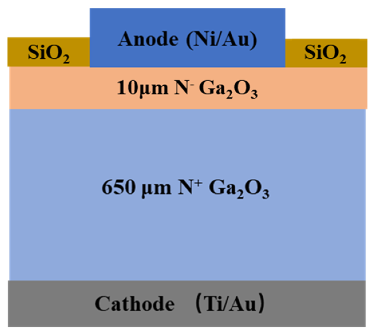
Figure 1 illustrates the cross-sectional schematic of the device. The epitaxial layer of the device was grown using halide vapor phase epitaxy (HVPE) technology, with a thickness of 10 μm and a doping concentration of 3.0 × 1016 cm−3. The substrate of the device consists of a 650 μm thick β-Ga2O3 single crystal. The cathode employs a Ti/Au (20/200 nm) ohmic contact, deposited via electron beam evaporation and subjected to rapid thermal annealing in a nitrogen (N2) atmosphere to significantly enhance the ohmic contact properties. The anode, on the other hand, utilizes a Ni/Au (50/200 nm) Schottky contact fabricated through a lift-off process. The entire device is packaged in a dual-pin TO configuration with an anode area of 4 mm2.
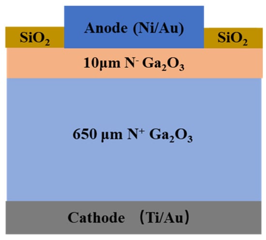
Figure 1.
Cross-sectional schematic of the β-Ga2O3 SBD device structure.
The high-temperature thermal oxidation process effectively reduces the oxygen vacancy concentration at the edge of the Schottky contact; the thermal oxidation treatment was conducted at a temperature of 400 °C for a duration of 20 min, thereby significantly lowering the peak electric field at the device edges and substantially increasing the breakdown voltage. The breakdown voltage of this SBD is approximately 650 V. This optimized design not only improves the device’s electrical performance but also enhances its reliability for high-power applications.
The X-ray irradiation experiments were conducted at the Xinjiang Technical Institute of Physics and Chemistry, Chinese Academy of Sciences. The experiments were performed at room temperature, with the device pins grounded. The X-rays used had an average energy ranging from 8 to 20 keV, a dose rate of 50 rad(Si)/s, and cumulative doses of 500 krad(Si), 1 Mrad(Si), and 2 Mrad(Si). There are a total of ten samples for the X-ray irradiation experiment, with one serving as a control and three each for the other three different irradiation fluences used in the experiment, with the experimental results being the average values. Noise information was extracted using the LS-PRO system before and after irradiation.
The neutron irradiation experiments were carried out at the Northwest Institute of Nuclear Technology. These experiments were also conducted at room temperature, with the device pins grounded. The devices were irradiated with 1 MeV neutrons at a fluence of 1 × 10¹³ n/cm2, the neutron irradiation fluence rate is 1 × 10⁹ n/cm2, and the irradiation time is 1000 s. After irradiation, bulk defect information was obtained using DLTS.
These experiments provide critical insights into the radiation-induced degradation mechanisms of β-Ga2O3 SBDs under both X-ray and neutron irradiation, contributing to a better understanding of their performance and reliability in radiation-rich environments.
3. Results and Discussion
- A.
- X-ray Irradiation
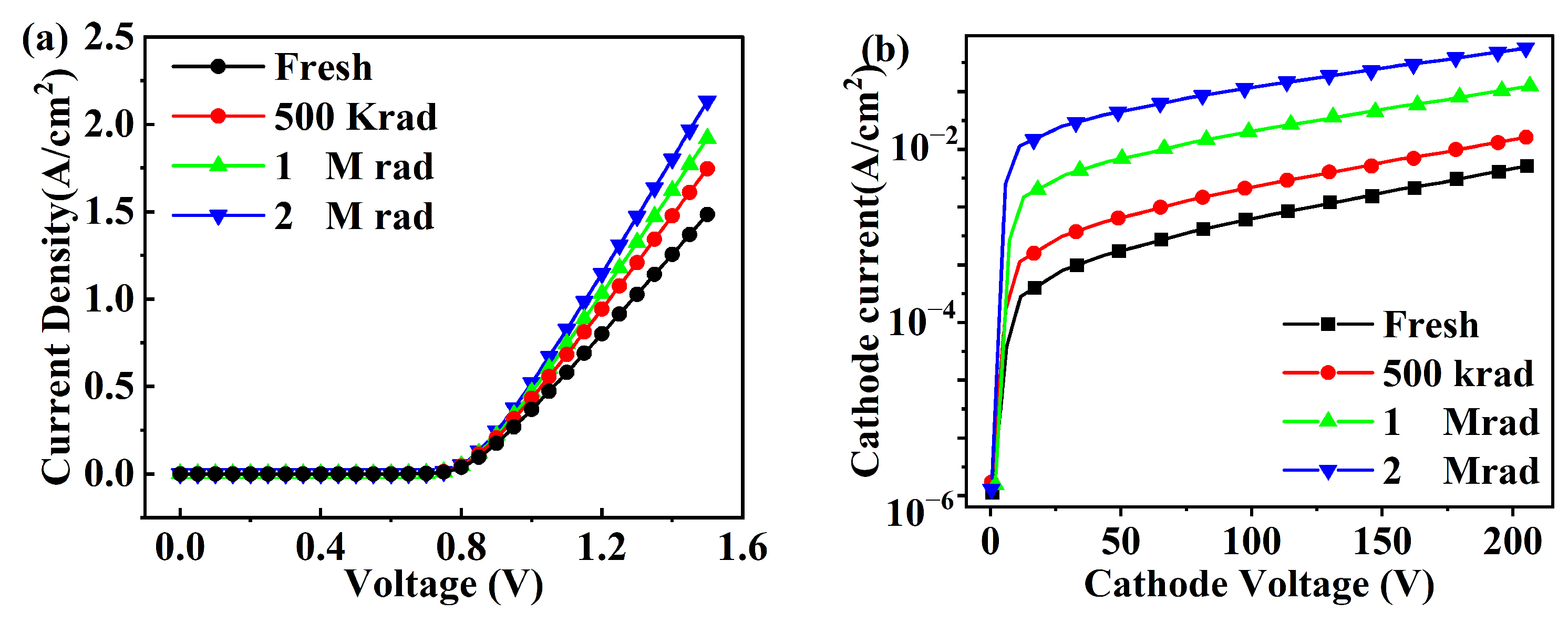
Figure 2a,b illustrate the forward and reverse electrical characteristics of the device before and after X-ray irradiation; in the figure, “Fresh” represents the sample before irradiation, and the three different doses are 500 krad, 1 Mrad, and 2 Mrad. It is evident from the figures that both the forward and reverse current densities of the device increase with the increasing irradiation dose. The forward current of the device is primarily associated with the thermionic emission mechanism related to the Schottky barrier height. Based on this mechanism, the ideal factor and Schottky barrier height of the device after X-ray irradiation were calculated using Equation (1) and Equation (2), respectively. In these equations, J represents the current density, A is the anode area of the device, T is the thermodynamic temperature (300 K at room temperature), q = 1.6 × 10⁻¹⁹ C is the electron charge, k is the Boltzmann constant, n is the ideality factor of the SBD, Js is the reverse saturation current density, A* is the Richardson constant, which is typically 40.8 A/(cm2·K2) for β-Ga2O3 material, and ϕ is the Schottky barrier height [14,15,16].
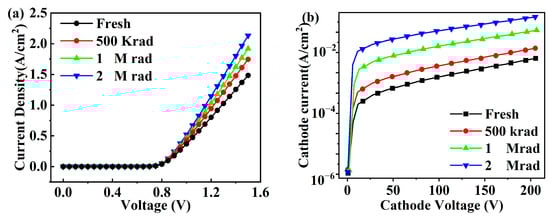
Figure 2.
Variations in the electrical properties of the device after X-ray irradiation: (a) forward current density; (b) reverse current density.
The calculations indicate that the Schottky barrier height ϕ decreases with the increasing irradiation dose, while the ideality factor n decreases with the increasing irradiation dose. The results are shown in Table 1. The reduction in the Schottky barrier height leads to an increase in the forward current density of the device, and simultaneously, it also increases the reverse current density.

Table 1.
Changes in device electrical parameters before and after irradiation.
The reverse current of the SBD is not only related to the current due to thermionic emission but also closely associated with the change in the carrier concentration in the epitaxial layer due to the variation in the concentration of internal defects in the material.
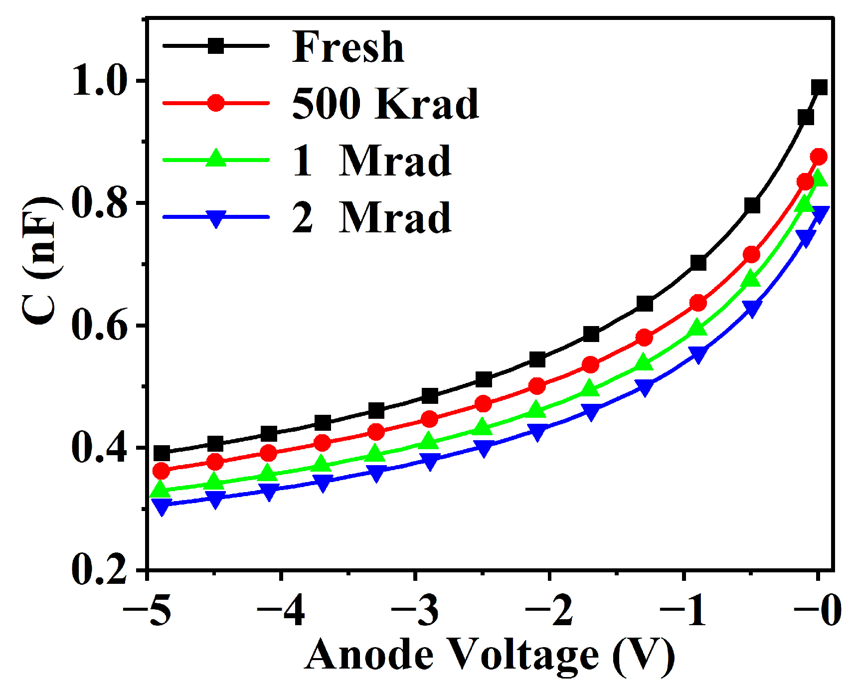
C-V measurement is a technique used to characterize the electrical properties of semiconductor materials or devices by analyzing the relationship between capacitance and voltage. It is particularly effective for determining the carrier concentration in SBDs. Under reverse bias conditions, the capacitance of an SBD is closely related to the carrier concentration. As the reverse bias voltage changes, the width of the depletion region varies accordingly, and this variation is reflected in the capacitance. By measuring these capacitance changes, the carrier concentration can be accurately inferred. Consequently, to evaluate the impact of irradiation on the device, we utilize the C-V characteristic curves of the β-Ga2O3 SBD before and after irradiation to calculate the changes in carrier concentration within the epitaxial layer. The C-V variation is shown in Figure 3. The calculation process follows Equations (3) and (4) [17,18,19]. In these equations, ND represents the carrier concentration, and ϵs is the relative permittivity of β-Ga2O3, which is 10.2, where is the vacuum permittivity with a value of 8.85 × 10⁻¹² F/m.
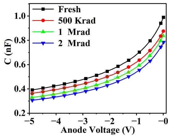
Figure 3.
Variation of C-V curves of the device under different X-ray irradiation doses.
The calculated results of the carrier concentration variation in the epitaxial layer of the device are shown in Table 2.
Table 2.
Carrier concentration before and after irradiation in the drift layer.
Table 2 shows that the carrier concentration of the device decreases significantly as the irradiation dose increases. When X-rays strike the device, they generate numerous electron–hole pairs in its epitaxial layer. Since electrons have higher mobility than holes, the generated holes tend to remain in the epitaxial layer and accumulate at the interface between the metal and semiconductor, forming interface defects. These defects capture carriers, leading to a reduction in the carrier concentration of the device.
Electrical characteristics provide insight into the internal structure and current conduction mechanisms of electronic devices, with changes in these characteristics indicating structural alterations. X-ray irradiation causes TID effects that damage β-Ga2O3 SBDs, leading to changes in their electrical properties, such as a decrease in the ideality factor and an increase in forward current density after the device is activated. Although these electrical parameters can characterize the radiation resistance of β-Ga2O3 diodes, their minimal changes make them less sensitive indicators of irradiation-induced alterations.
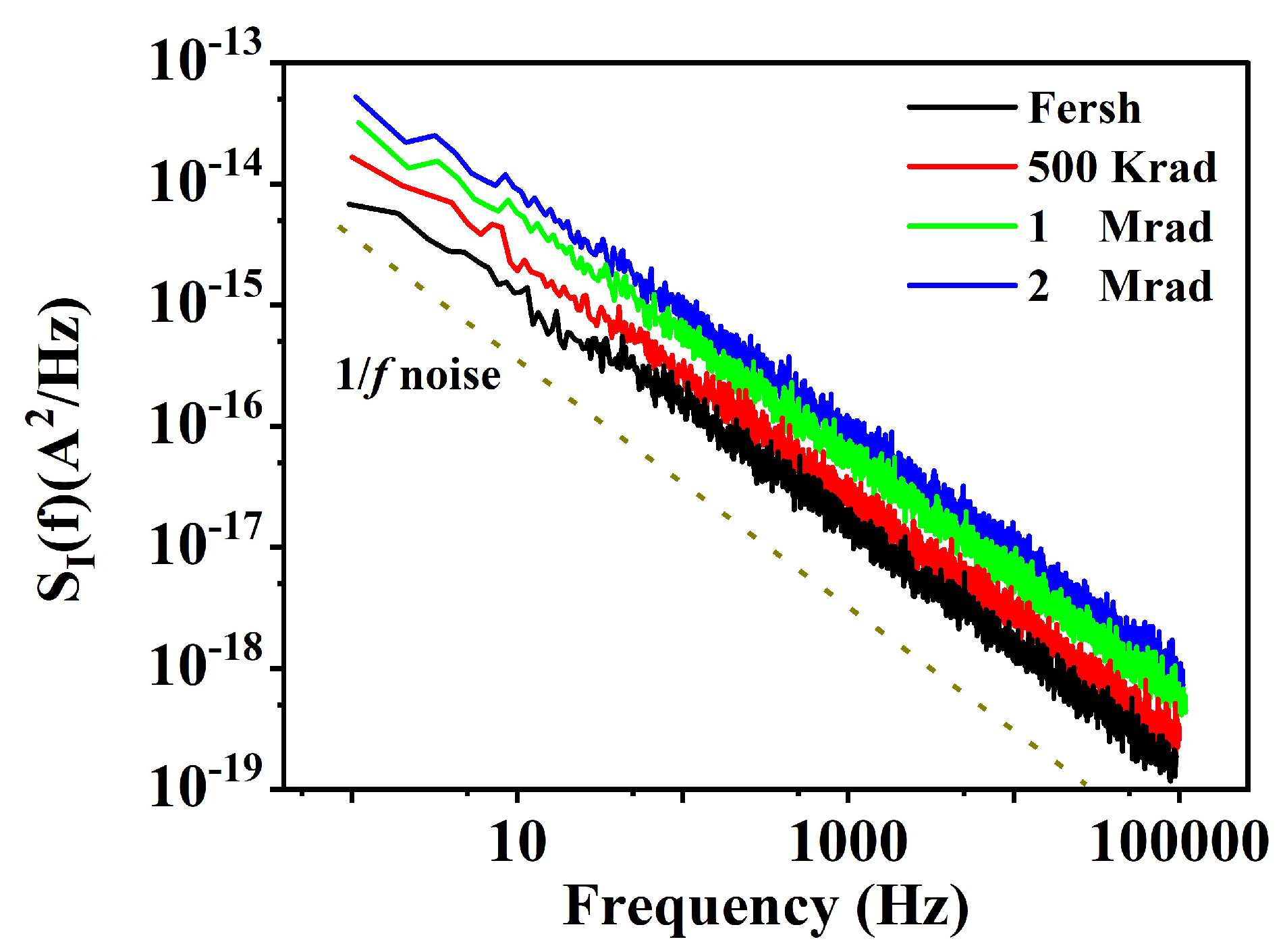
In contrast, noise is increasingly recognized as a highly sensitive method for detecting potential internal defects in devices. It offers a rapid and non-destructive testing approach [20,21]. When changes occur in the device’s original lattice structure, electron state density, or impurity distribution over time or under stress, noise detection exhibits more significant variations compared to other structure-sensitive parameters [22]. Noise in electronic devices is highly sensitive to these defects, making noise testing a common method for diagnosing and predicting defect changes [23]. Numerous studies have shown that 1/f noise serves as a sensitive parameter reflecting defect information in electronic components [24]. Therefore, when studying defects and interface state changes in the space charge region and near the oxide–semiconductor interface after irradiation, noise diagnostic techniques more effectively reflect the extent of radiation damage than traditional electrical parameters, as shown in Figure 4.
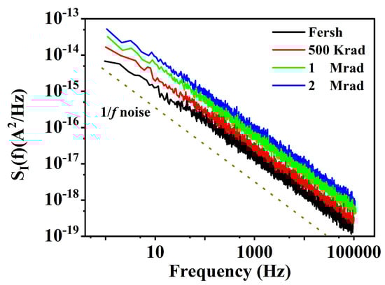
Figure 4.
Variation of low-frequency noise power spectral density of the device with irradiation dose.
The current noise density spectrum induced by interface defects can be expressed using the formula proposed by Jantsch et al. [25]. The expression for the current noise power spectral density is as follows.
The current noise power spectral density can be described by the following equation proposed by Jantsch et al. [25], where G is a constant with a value of 0.1, Dis is the density of interface states, q = 1.6 × 10⁻¹⁹ C is the electron charge, k is the Boltzmann constant, and β is a parameter describing the carrier transport mechanism in the Schottky barrier diode (SBD). For the thermionic emission mechanism, β = qkT, f is the frequency at which the noise is measured, I is the forward current during the measurement, is the permittivity of β-Ga2O3, Nd is the doping concentration after irradiation, h is the Planck constant, W is the width of the space-charge region, and A is the effective contact area of the device.
It is evident that besides the doping concentration, the density of interface states is a key factor affecting noise power spectral density. At higher irradiation doses, the concentration of interface defects within the device increases, leading to a rise in noise power spectral density.
- B.
- Neutron Irradiation
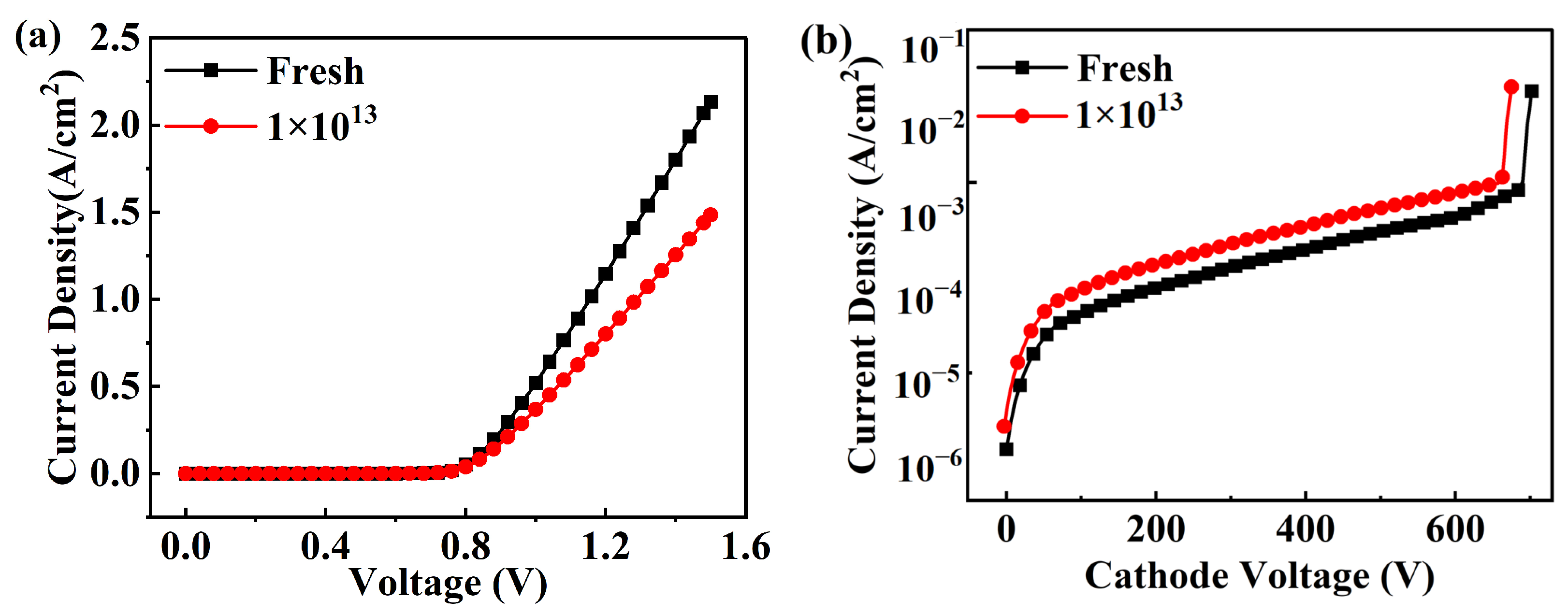
Figure 5 illustrates the changes in the device’s forward and reverse electrical performance before and after neutron irradiation; in the figure, “Fresh” represents the sample before irradiation, and the neutron irradiation fluence is 1 × 10¹³ n/cm2, denoted as 1 × 10¹³ in the figure.
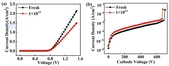
Figure 5.
Variations in the electrical properties of the device before and after neutron irradiation: (a) forward current density; (b) reverse current density.
As shown in Figure 5, the electrical characteristics of the device after neutron irradiation differ from those after X-ray irradiation. The forward current density of the device decreases while the reverse current density increases. Calculations using Equations (1) and (2) reveal that the SBH of the device decreases from 1.12 eV to 1.09 eV, and the ideality factor decreases from 1.17 to 1.10, with relatively small changes. In the research by Yue et al. [26]., it was suggested that the degradation of the device’s electrical properties after neutron irradiation is not due to the influence of interface defects.
Neutrons, as highly penetrating particles, interact with atoms in the β-Ga2O3 material, displacing them from their lattice positions and creating vacancies. If the vacancies and interstitial atoms are still influenced by their elastic and Coulomb fields, they may recombine. However, if they exceed the range of these fields, they can form interstitial-vacancy pairs, i.e., Frenkel defects. These defects can lead to device performance degradation or permanent damage. Therefore, the degradation of the device’s electrical properties after irradiation may be caused by changes in the bulk defect concentration induced by neutron irradiation.
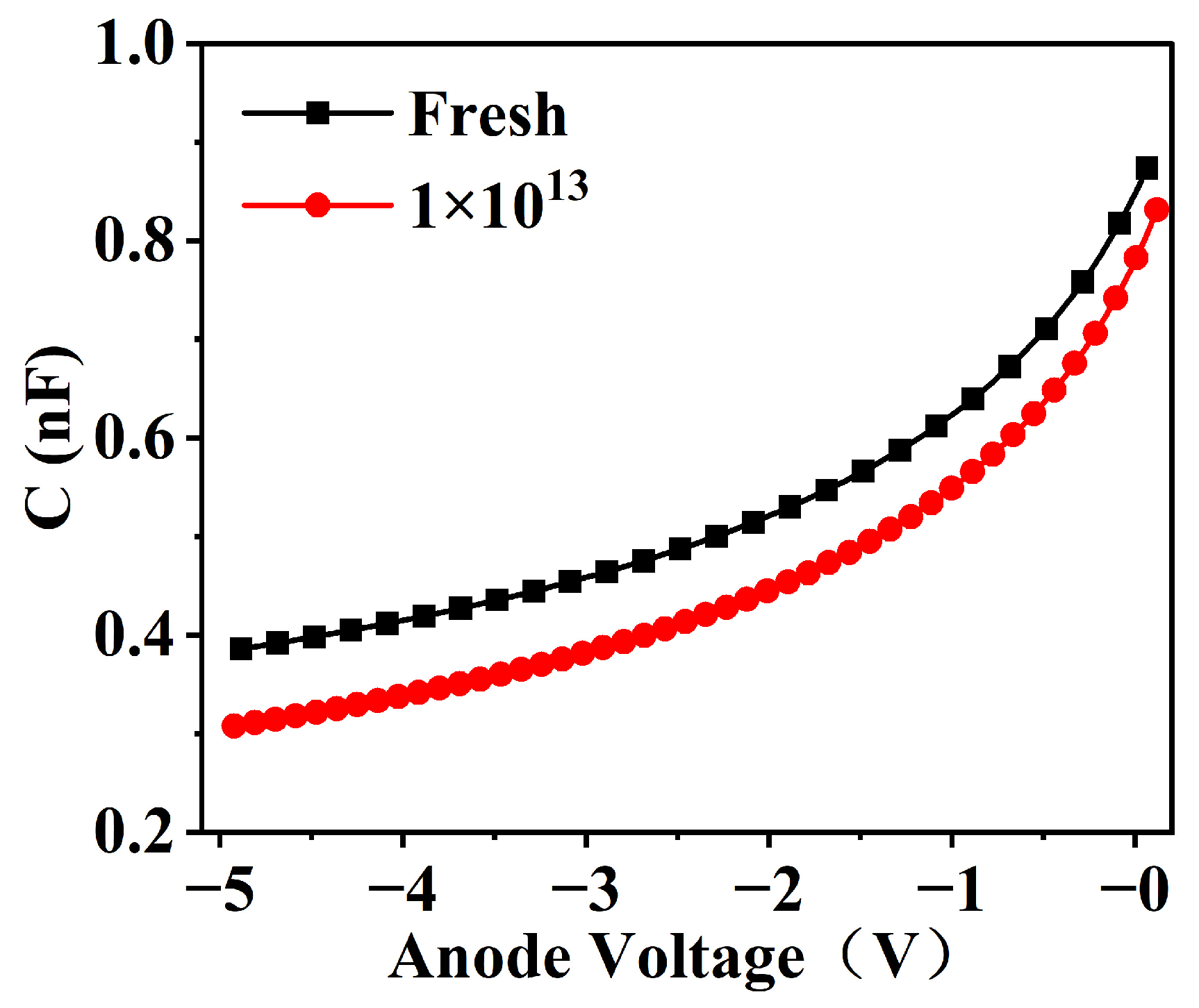
Figure 6 shows the variation in capacitance of the device before and after irradiation. Through the change in C-V characteristics, it was calculated that the carrier concentration of the device decreased from 8.328 × 1015 cm−3 to 7.734 × 1015 cm−3 after neutron irradiation. This reduction in carrier concentration is the direct cause of the decrease in the device’s forward current.
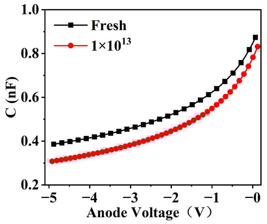
Figure 6.
Variation of capacitance of the device before and after neutron irradiation.
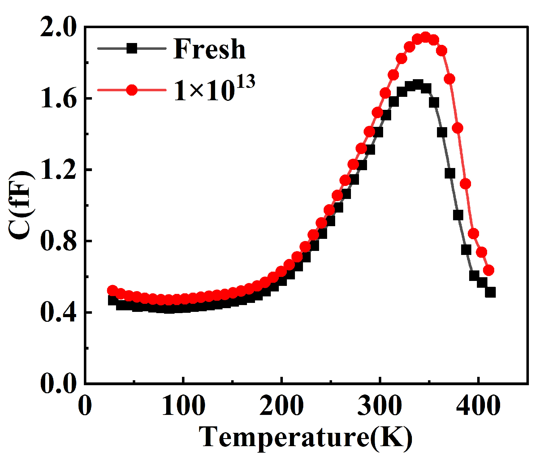
The reduction in carrier concentration is attributed to the carrier removal effect of bulk defects. DLTS is a powerful and widely used technique for characterizing deep-level defects in semiconductors. It operates by applying a voltage pulse to the sample, which captures carriers (electrons or holes) into deep-level traps within the material. The subsequent release of these trapped carriers generates a transient current signal that is measured as a function of temperature. By analyzing the temperature dependence of these transient signals, DLTS can provide detailed information on the energy levels and concentrations and capture cross-sections of deep-level defects. This non-destructive and highly sensitive method is essential for understanding the electronic properties of semiconductor materials and devices, particularly in the context of quality control and fundamental research. To verify this, we conducted validation using DLTS defect spectra. During the test, the reverse voltage (UR) was set at −5 V, the UP at 10 V, the TW at 7 s, and the pulse width (TP) at 1 ms. The test results are shown in Figure 7.

Figure 7.
DLTS defect spectra of the device before and after neutron irradiation.
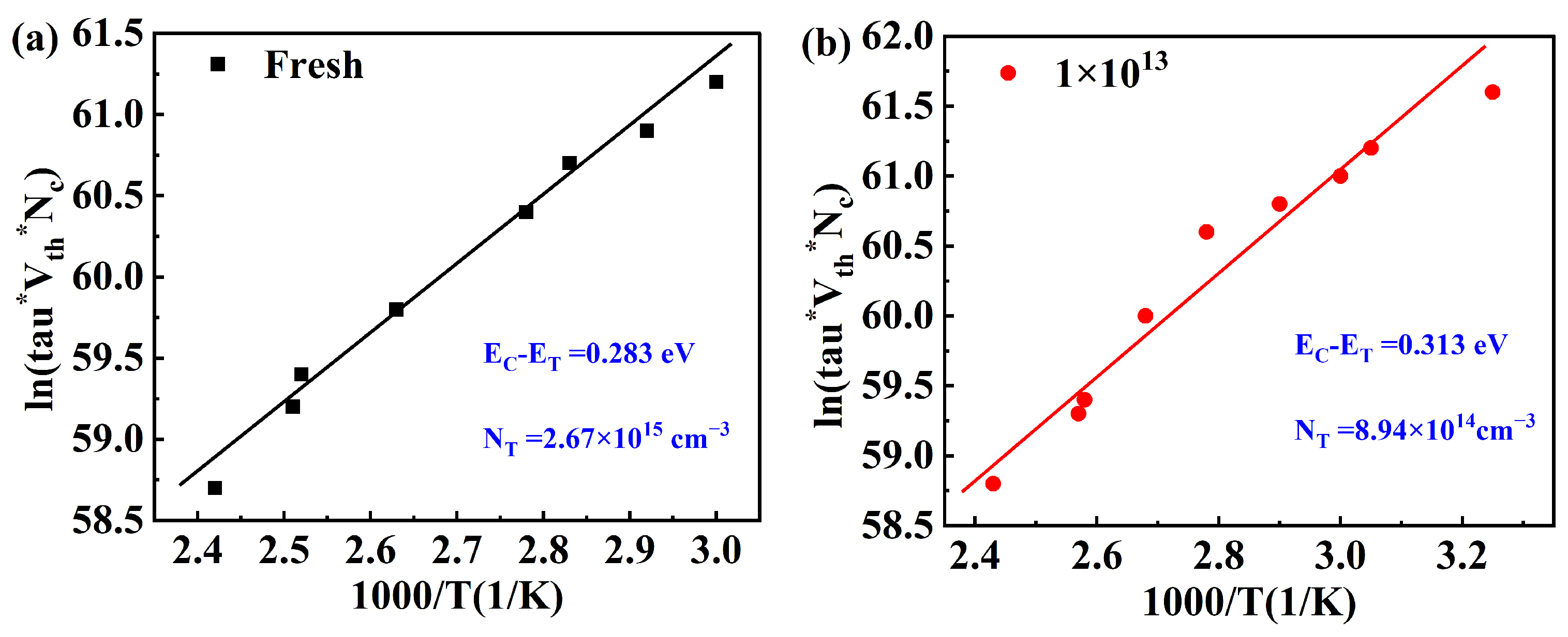
As can be observed from the figure, the temperature at which the defects within the device are excited remains the same after irradiation, indicating that the defect energy levels have not changed. However, the peak value of the vertical axis in the DLTS spectra increased from 1.64 fF to 1.97 fF after irradiation, which suggests an increase in defect concentration. The defect energy levels and concentrations can be determined through the Arrhenius linear relationship plot, as shown in Figure 8. Before irradiation, the primary defect within the device had an energy level depth of Ec−0.28 eV, with a defect concentration of 2.67 × 1015cm−3. After irradiation, the defect energy level deepened to Ec−0.31 eV, and the defect concentration decreased to 8.94 × 1014 cm−3.
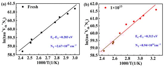
Figure 8.
(a) Arrhenius plot of the energy levels of the device before irradiation. (b) Arrhenius plot of the energy levels of the device after irradiation.
The DLTS spectra unveiled the emergence of specific defect states introduced by neutron irradiation, which function as carrier traps and substantially influence the carrier concentration within the material. This observation corroborates the reduction in carrier concentration following neutron irradiation, thereby affirming that the bulk defects generated by neutron irradiation are the primary cause of the carrier removal effect.
- C.
- TCAD Simulation
TCAD (Technology Computer-Aided Design) simulation is a powerful tool in the semiconductor industry for the development, optimization, and characterization of semiconductor devices and processes. It provides a comprehensive framework for various aspects of semiconductor manufacturing, including the simulation of process steps, device structures, and electrical performance. TCAD tools, such as those from Silvaco and Synopsys, can model complex physical phenomena, optimize device performance, and predict the impact of process variations on device characteristics. These simulations are crucial for understanding the behavior of advanced semiconductor devices. TCAD is also used for device optimization and reliability analysis.
Therefore, to theoretically validate our experimental results, we performed two-dimensional numerical simulations of the SBD devices after neutron irradiation using the Sentaurus 2018 TCAD software. To ensure the accuracy of the simulation results, we employed a variety of physical models, including the Shockley–Read–Hall (SRH) recombination model, high-field saturation model, thermionic emission model, Auger recombination model, and bandgap narrowing model. The material parameters of gallium oxide used in the simulation were derived from previous studies and are specifically summarized in Table 3.
Table 3.
β-Ga2O3 material parameters used in simulation [27,28,29].
After completing the simulation parameter settings, we first conducted a simulation of the TID induced by X-ray irradiation and extracted the relevant physical parameters of the device. The results are shown in Figure 9.
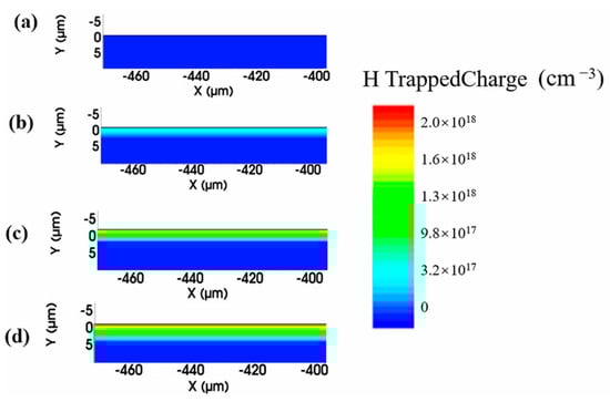
Figure 9.
Distribution of hole-trapped charge inside the device after X-ray irradiation at different doses: (a) Fresh, (b) 500 Krad, (c) 1 Mrad, and (d) 2 Mrad.
Figure 9 illustrates that the hole density in the device’s epitaxial layer increases with higher radiation doses, aligning closely with our experimental findings. The simulation results of the device’s current density distribution are shown in Figure 10.
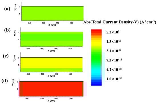
Figure 10.
Distribution of total current density inside the device after X-ray irradiation at different doses: (a) Fresh, (b) 500 Krad, (c) 1 Mrad, and (d) 2 Mrad.
As shown in Figure 10, the simulation results indicate that the internal current density of the device increases with the increase in irradiation dose. In conjunction with the analysis of Figure 2b and Figure 9, this increase is attributed to the higher concentration of interface defects caused by the TID. This finding corroborates our experimental results.
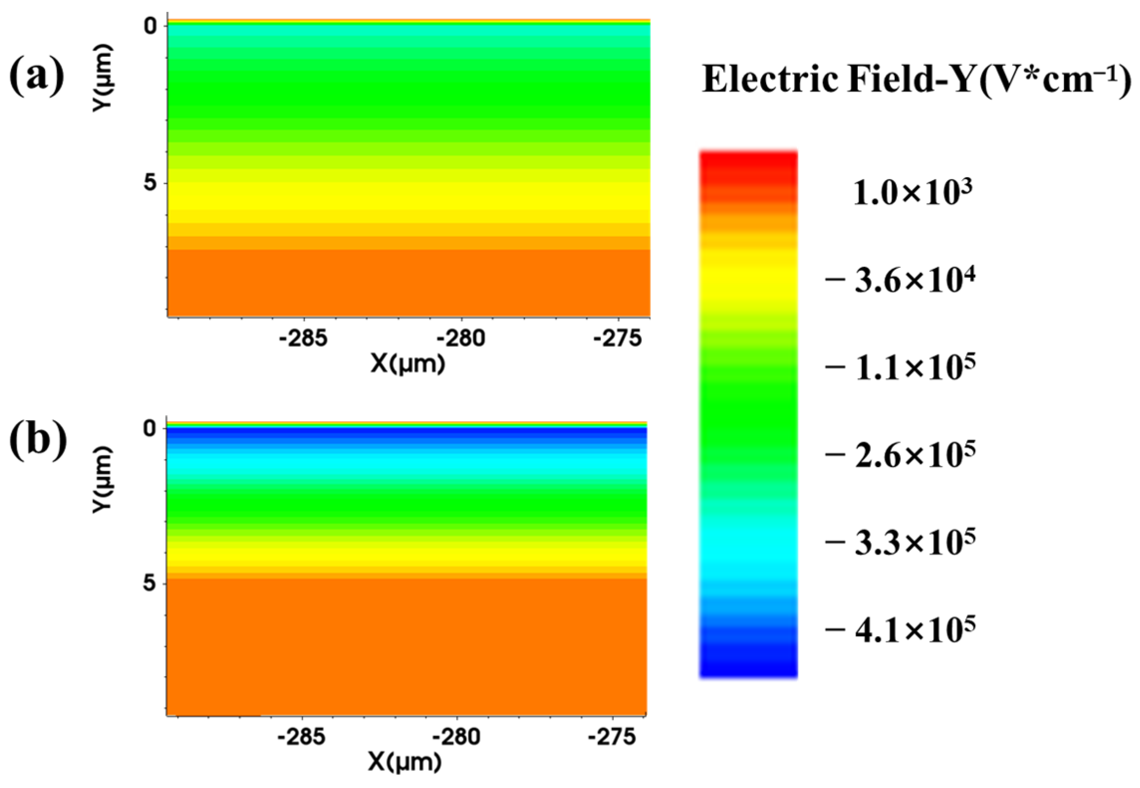
During the neutron irradiation simulation, since the defect energy levels remained almost unchanged before and after irradiation, we added defects with an energy level of Ec−0.3 eV to the device both before and after irradiation. The defect concentration in the device before irradiation was set to 2.67 × 1015 cm−3, and the defect concentration in the device after irradiation was set to 8.94 × 1014 cm−3. This approach allowed us to more accurately simulate the experimental results. The simulation results are shown in Figure 11.

Figure 11.
Illustration of the electric field intensity distribution within the epitaxial layer under a reverse bias of 100 V both before and after irradiation: (a) pre-irradiation and (b) post-irradiation.
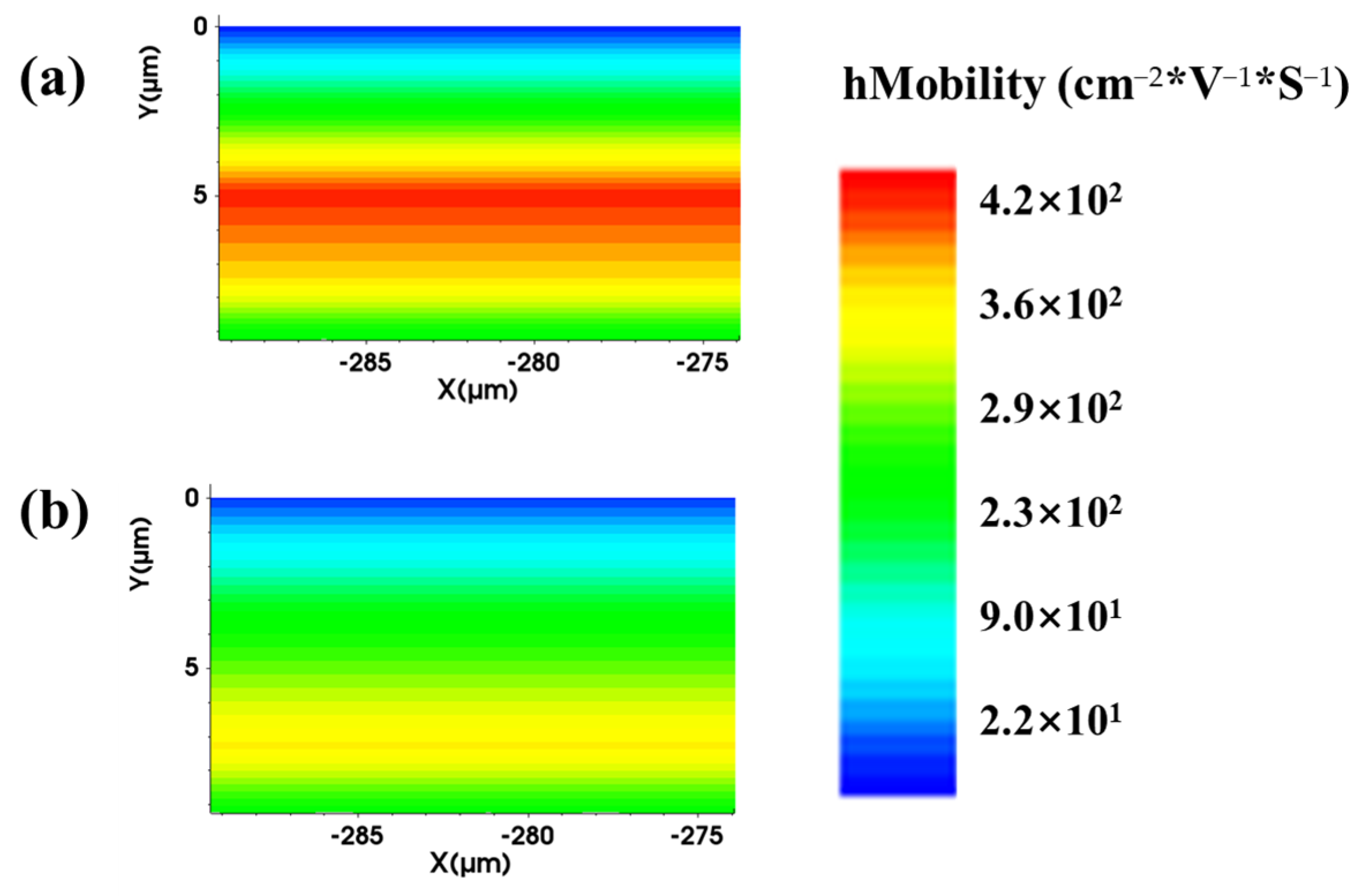
As illustrated in Figure 11, after introducing defects into the device, a reverse bias voltage of 100 V was applied. The electric field intensity in the sensitive region of the epitaxial layer post-irradiation was observed to be higher compared to the pre-irradiation state. This finding is consistent with the neutron irradiation results shown in Figure 5b. Neutron irradiation generates a significant number of lattice defects in semiconductor materials. These defects, including vacancies, interstitial atoms, and complex defects, disrupt the periodic structure of the lattice, leading to increased carrier scattering and a consequent reduction in carrier mobility. To further investigate this effect, the hole mobility in the epitaxial layer region was extracted both before and after irradiation, as shown in Figure 12.
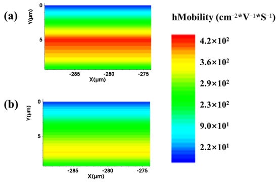
Figure 12.
The simulation results of the change in hole mobility in the device before and after neutron irradiation: (a) before irradiation and (b) after irradiation.
As shown in Figure 12, after irradiation, the mobility of holes and other defects decreases, which leads to an increase in the local electric field inside the device. Meanwhile, acting as leakage channels, they enhance the reverse current density, thereby reducing the breakdown voltage of the device and affecting its reliability.
In summary, neutron irradiation introduces a large number of lattice defects, such as vacancies and interstitial atoms, into the semiconductor material of the diode. These defects disrupt the crystal structure of the material, leading to a decrease in carrier mobility and an increase in recombination rates. Since these defects are randomly and disorderly distributed, it is almost impossible to restore the material to its pre-irradiation ordered state. This results in a decline in the forward current transport performance of the diode and an increase in the reverse leakage current. These changes are irreversible because the defects introduced by irradiation permanently alter the carrier transport paths and recombination mechanisms.
4. Conclusions
This study examines the degradation of electrical properties in β-Ga2O3 SBDs due to varying doses of X-ray irradiation using both experimental and simulation methods. The results indicate that the degradation of device performance is associated with interface defects induced by the TID of X-rays. In contrast, neutron irradiation primarily causes displacement damage in the devices. DLTS characterization revealed that the energy levels of bulk defects caused by displacement damage remain unchanged, but their concentration increases. The carrier removal effect induced by these bulk defects reduces the forward current density of the devices after neutron irradiation. Meanwhile, these defects serve as leakage channels, leading to an increase in reverse current density, a decrease in carrier mobility inside the device, and a reduction in the breakdown voltage of the device. By employing the TCAD two-dimensional simulation tool, this study investigates the effects of TID and displacement damage on devices exposed to varying doses of X-ray and neutron irradiation. The simulation results demonstrate strong consistency with experimental observations, validating the accuracy of the computational approach. Furthermore, the findings shed light on the degradation mechanisms affecting the electrical properties of β-Ga2O3 under radiation exposure, offering valuable insights for enhancing the radiation tolerance of β-Ga2O3 devices. These results provide a foundation for optimizing radiation-hardening processes in future device development.
Author Contributions
Methodology, W.F.; Validation, X.T.; Writing—original draft, P.Z.; Writing—review & editing, T.M. All authors have read and agreed to the published version of the manuscript.
Funding
This research was funded by the fund of the GuangDong Basic and Applied Basic Research Foundation (No. 2022A1515111049) and the National Natural Science Foundation of China (No. 12305299).
Data Availability Statement
The datasets presented in this article are not readily available because the data are part of an ongoing study.
Acknowledgments
We gratefully acknowledge the technical support provided by Xi’an Jiaotong University and Science and Technology on Reliability Physics and Application of Electronic Component Laboratory.
Conflicts of Interest
The authors declare no conflicts of interest.
References
- Higashiwaki, M.; Sasaki, K.; Kuramata, A.; Masui, T.; Yamakoshi, S. Gallium oxide (Ga2O3) metal-semiconductor field-effect transistors on single-crystal β-Ga2O3 (010) substrates. Appl. Phys. Lett. 2012, 100, 013504. [Google Scholar] [CrossRef]
- Pearton, S.J.; Yang, J.; Cary, P.H.; Ren, F.; Kim, J.; Tadjer, M.J.; Mastro, M.A. A review of Ga2O3 materials, processing, and devices. Appl. Phys. Rev. 2018, 5, 011301. [Google Scholar] [CrossRef]
- Green, A.J.; Chabak, K.D.; Heller, E.R.; Fitch, R.C.; Baldini, M.; Fiedler, A.; Jessen, G.H. β-Ga2O3 MOSFETs for radio frequency operation. IEEE Electron Device Lett. 2016, 37, 902–905. [Google Scholar] [CrossRef]
- Wong, M.H.; Sasaki, K.; Kuramata, A.; Yamakoshi, S.; Higashiwaki, M. Field-plated Ga2O3 MOSFETs with a breakdown voltage of over 750 V. IEEE Electron Device Lett. 2016, 37, 212–215. [Google Scholar] [CrossRef]
- Zhang, Y.; Joishi, C.; Xia, Z.; Brenner, M.; Lodha, S.; Rajan, S. Demonstration of high mobility and quantum transport in modulation-doped β-(AlxGa1−x)2O3/Ga2O3 heterostructures. Appl. Phys. Lett. 2018, 112, 173502. [Google Scholar] [CrossRef]
- Chen, X.; Ren, F.; Gu, S.; Ye, J. Review of gallium oxide based field-effect transistors and Schottky barrier diodes. Chin. Phys. B 2019, 28, 017105. [Google Scholar]
- Oh, S.; Jung, Y.; Mastro, M.A.; Kim, J.; Ren, F. Radiation effects in Ga2O3 materials and devices. J. Mater. Chem. C 2020, 8, 13054–13065. [Google Scholar]
- Ahmadi, E.; Oshima, Y.; Wu, F. Radiation damage effects in Ga2O3 materials and devices. J. Appl. Phys. 2020, 127, 131101. [Google Scholar]
- Wu, C.; Wu, F.M.; Hu, H.Z.; Wang, S.L.; Liu, A.P.; Guo, D.Y. Radiation-induced gallium vacancy defects and carrier mobility degradation in β-Ga2O3 photodetectors. Mater. Today Phys. 2022, 28, 100883. [Google Scholar] [CrossRef]
- Polyakov, A.Y.; Smirnov, N.B.; Govorkov, A.V.; Pearton, S.J. Fast neutron irradiation effects in n-GaN and β-Ga2O3. J. Vac. Sci. Technol. B 2007, 25, 436–442. [Google Scholar] [CrossRef]
- Pearton, S.J.; Ren, F.; Patrick, E.; Law, M.E.; Polyakov, A.Y. Review—Ionizing radiation damage effects on GaN and β-Ga2O3 devices. ECS J. Solid State Sci. Technol. 2016, 5, Q35–Q60. [Google Scholar]
- Cai, Z.; He, X.; Wang, K.; Long, H. Enhancing Performance of GaN/Ga2O3 p-n Junction UVC Photodetectors via Interdigitated Structure. Small Methods 2023, 7, 2301148. [Google Scholar]
- Higashiwaki, M.; Sasaki, K.; Kuramata, A.; Masui, T.; Yamakoshi, S. Development of gallium oxide power devices. Phys. Status Solidi A 2014, 211, 21–26. [Google Scholar]
- Liu, M.; Hua, M.; Tian, X.; Wang, Z.; Gao, H.; Wang, W.; Chen, Y.; Zhang, C.; Zhao, S.; Feng, Q.; et al. Effect of gamma irradiation on β-Ga2O3 vertical Schottky barrier diode. Appl. Phys. Lett. 2023, 123, 212103. [Google Scholar] [CrossRef]
- Holmes-Siedle, A.G.; Adams, L. Handbook of Radiation Effects; Oxford University Press: Oxford, UK, 1993. [Google Scholar]
- Sheoran, H.; Kumar, V.; Singh, R. A Comprehensive Review on Recent Developments in Ohmic and Schottky Contacts on Ga2O3 for Device Applications. ACS Appl. Electron. Mater. 2022, 4, 2589–2628. [Google Scholar] [CrossRef]
- Sze, S.M.; Li, Y.; Ng, K.K. Physics of Semiconductor Devices; Nework Wiley: Hoboken, NJ, USA, 1981. [Google Scholar]
- Zheng, X.-F.; Dong, S.-S.; Ji, P.; Wang, C.; He, Y.-L.; Lv, L.; Ma, X.-H.; Hao, Y. Characterization of bulk traps and interface states in AlGaN/GaN heterostructure under proton irradiation. Appl. Phys. Lett. 2018, 112, 233504. [Google Scholar] [CrossRef]
- Ai, W.-S.; Liu, J.; Feng, Q.; Zhai, P.-F.; Hu, P.-P.; Zeng, J.; Zhang, S.-X.; Li, Z.-Z.; Liu, L.; Yan, X.-Y.; et al. Degradation of β-Ga2O3 Schottky barrier diode under swift heavy ion irradiation. Chin. Phys. B 2021, 30, 056110. [Google Scholar] [CrossRef]
- Vandamme, L.K.J.; Li, X.; Rigaud, D. 1/f noise in MOS devices, mobility fluctuations, and number fluctuations. IEEE Trans. Electron Devices 1994, 41, 1936–1945. [Google Scholar]
- Hooge, F.N. 1/f noise sources. IEEE Trans. Electron Devices 1994, 41, 1926–1935. [Google Scholar]
- Simoen, E.; Claeys, C. On the flicker noise in submicron silicon MOSFETs. Solid-State Electron. 1999, 43, 865–882. [Google Scholar]
- Balandin, A.A. Low-frequency 1/f noise in graphene devices. Nat. Nanotechnol. 2013, 8, 549–555. [Google Scholar] [PubMed]
- Fleetwood, D.M. Radiation effects in a fluctuating world: The role of noise in semiconductor devices and circuits. IEEE Trans. Nucl. Sci. 2018, 65, 1465–1481. [Google Scholar]
- Jantsch, O. Flicker (1/f) noise generated by a random walk of electrons in interfaces. IEEE Trans. Electron Devices 1987, 34, 1100–1115. [Google Scholar] [CrossRef]
- Yue, S.; Zheng, X.; Hong, Y.; Zhang, X.; Zhang, F.; Wang, Y.; Ma, X.; Hao, Y. Effects of Neutron Irradiation on Electrical Performance of β-Ga2O3 Schottky Barrier Diodes. IEEE Trans. Electron Devices 2023, 70, 3026–3030. [Google Scholar] [CrossRef]
- Ma, H.; Wang, W.; Cai, Y.; Wang, Z.; Zhang, T.; Feng, Q.; Chen, Y.; Zhang, C.; Zhang, J.; Hao, Y. Analysis of single event effects by heavy ion irradiation of Ga2O3 metal–oxide–semiconductor field-effect transistors. J. Appl. Phys. 2023, 133, 084501. [Google Scholar] [CrossRef]
- Wong, H.Y.J. TCAD simulation models, parameters, and methodologies for β-Ga2O3 power devices. ECS J. Solid State Sci. Technol. 2023, 12, 045001. [Google Scholar]
- Zhou, H.; Zeng, S.; Zhang, J.; Liu, Z.; Feng, Q.; Xu, S.; Zhang, J.; Hao, Y. Comprehensive study and optimization of implementing p-NiO in β-Ga2O3 based diodes via TCAD simulation. Crystals 2021, 11, 1186. [Google Scholar] [CrossRef]


Disclaimer/Publisher’s Note: The statements, opinions and data contained in all publications are solely those of the individual author(s) and contributor(s) and not of MDPI and/or the editor(s). MDPI and/or the editor(s) disclaim responsibility for any injury to people or property resulting from any ideas, methods, instructions or products referred to in the content. |
© 2025 by the authors. Licensee MDPI, Basel, Switzerland. This article is an open access article distributed under the terms and conditions of the Creative Commons Attribution (CC BY) license (https://creativecommons.org/licenses/by/4.0/).