Article

Advancing Mapping Strategies and Circuit Optimization for Signed Operations in Compute-in-Memory Architecture

1
School of Electronics and Information, Northwestern Polytechnical University, Xi’an 710072, China
2
The 58th Research Institute of China Electronics Technology Group Corporation, Wuxi 214035, China
3
School of Microelectronics, Xi’an Jiaotong University, Xi’an 710049, China
*
Author to whom correspondence should be addressed.
Electronics 2025, 14(7), 1340; https://doi.org/10.3390/electronics14071340
Submission received: 5 March 2025 / Revised: 25 March 2025 / Accepted: 26 March 2025 / Published: 27 March 2025
(This article belongs to the Section Circuit and Signal Processing)

Abstract

:
Compute-in-memory (CIM) is a key focus in chip design, with mapping strategies gaining attention. However, many studies overlook the arrangement of significant bits in weights and the influence of the input order of activation bits, which are key aspects of bit-level mapping strategies. While the three existing bit-level mapping strategies have their respective application scenarios and can address the majority of cases through combined use, a major challenge remains: their lack of support for signed computations, which limits their applicability in many practical scenarios. This work improves three existing mapping strategies to support signed weights and activations, optimizing CIM peripheral circuits with minimal overhead. The experimental results show a 68.4% improvement in energy efficiency and 56.2% in speed with a less than 1% area increase on Yolov3-tiny, and a 4 × and 3.59 × boost in energy efficiency using input-side parallel mapping strategy (ISP) and input- and output-side parallel mapping strategy (IOSP) on a single layer. The proposed work has the potential to significantly advance the field of CIM-based neural network accelerators by enabling efficient signed computations and enhancing flexibility, paving the way for broader adoption in real-time and energy-constrained applications.

1. Introduction

Compute-in-memory has emerged as a promising paradigm to address the growing challenges of data-intensive applications in fields such as artificial intelligence and machine learning. Traditional von Neumann architectures are increasingly bottlenecked by the data movement between memory and processing units, often referred to as the “memory wall”. CIM seeks to mitigate this by integrating computation directly within memory arrays, drastically reducing data transfer latency and power consumption. As a result, CIM offers a significant advantage for workloads characterized by large-scale matrix operations and high parallelism, which are common in neural network models.
Weight data mapping strategies and data flow scheduling are crucial aspects of CIM architectures, as they largely determine the achievable level of parallelism. Since introducing the conventional mapping strategy (CMS) [1], researchers have continuously developed new strategies for improving data reuse and array utilization. Some methods demonstrate significant improvements for small convolutional kernels [2,3,4], while others focus on large kernels [5,6]. However, since convolutional kernels within a network vary in size, maximizing both array utilization and parallelism simultaneously becomes challenging. As a result, researchers often employ multiple strategies within the same network [7].
Nevertheless, when proposing new data mapping strategies, most approaches treat each number in the weight matrix as an indivisible unit, overlooking the specific arrangement of significant bits within each number across the array. In contrast, the bit-level mapping strategy addresses this limitation by considering the individual bits within each number, operating in parallel with the data mapping strategy. While the two strategies function independently, both significantly impact the computational efficiency of compute-in-memory arrays.
Bai et al. [8] summarized and proposed three different bit-level mapping strategies: the serial bit input parallel weight mapping strategy (SBIPW), input-side parallel mapping strategy (ISP), and input- and output-side parallel mapping strategy (IOSP). Among these, SBIPW is the most commonly used and has been widely adopted in various studies. As illustrated in Figure 1, the significant bits of the weight data are arranged in descending order along the same row, and the input data’s significant bits are fed sequentially, either from high to low or vice versa. The final result is obtained by accumulating the outputs over multiple cycles. This approach is straightforward and effective, without requiring complex peripheral circuitry, but it suffers from limited flexibility. The ISP and IOSP methods, in contrast, are tailored to bit-level mapping for convolutional kernels of different shapes, with their mechanisms discussed in the following section.
Another challenge closely tied to the bit-level mapping process is handling both signed input and signed weight. Due to the unique computation and output readout mechanisms in CIM arrays, the sign bit of W contributes to different partial results, making direct summation challenging. As a result, direct multiply–accumulate (MAC) operations on signed numbers are not feasible, as shown in Equation (1). The most common solution is to divide the input matrix into positive and negative parts and compute them separately. However, this approach incurs significant overhead in terms of area or latency. Alternative methods include modifying the encoding of weights [9,10,11] or enhancing the cell and array circuits to support signed MAC [12,13,14]. While these approaches reduce the overhead, they often lack flexibility and introduce excessive complexity for handling signed computations. You et al.’s work [15] offers a more efficient solution, allowing seamless switching between signed and unsigned operations with minimal cost. However, even in their approach, the input data still need to be split into positive and negative components.
( W × X ) = i = 0 n 1 ( W · X i ) · 2 i
To address the insufficient support for signed operations and the lack of flexibility in existing bit-level mapping strategies, we propose a new set of optimizations. The contributions of this work can be summarized as follows:
  • We enhanced the existing ISP and IOSP mapping strategies to accommodate both signed/unsigned weights and signed/unsigned inputs in both DCIM and analog CIM.
  • We modified the wiring of the adder tree and shift adders in DCIM architecture to enable the macro to support signed operation in SBIPW, ISP, and IOSP mapping strategies with minimal cost.
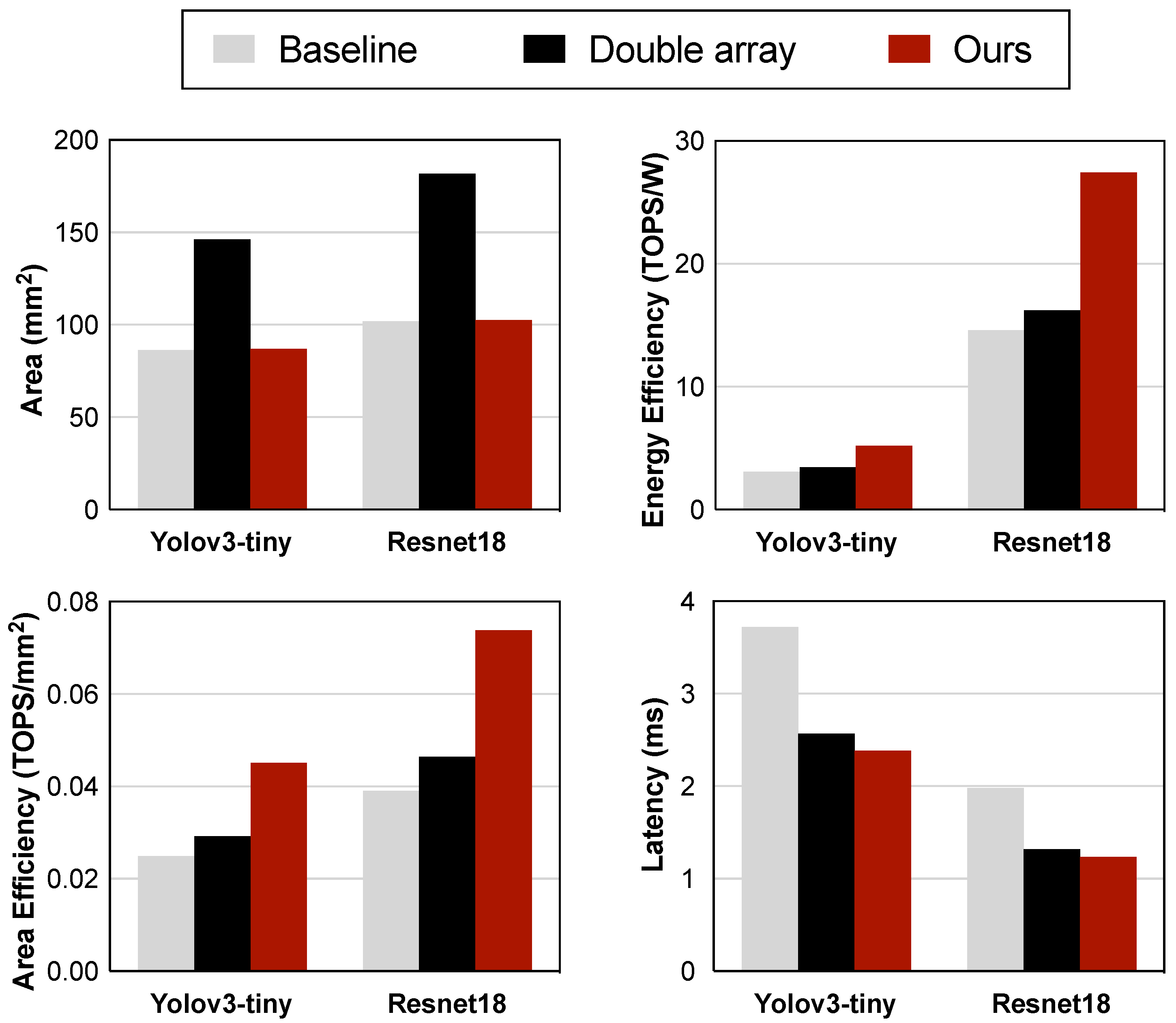
  • We conducted performance validation of the improved array using the latest NeuroSim V1.4 [16], which facilitates the simulation of DCIM architectures. The results demonstrate that our enhancements to ISP and IOSP achieve a 4× and 3.59× improvement in energy efficiency for single-layer networks, respectively. The combined use of the three strategies in testing on Yolov3-tiny also achieved a 68.4% boost in energy efficiency and a 56.2% increase in speed.
The organization of this paper is as follows: Section 2.1, Section 2.2 and Section 2.3 describe the three improved bit-level mapping strategies proposed in this work. Section 2.4 presents the optimized peripheral circuits. Section 3 demonstrates the experimental results of the enhanced bit-level mapping strategies. Finally, Section 4 concludes this paper.

2. The Proposed Bit-Level Mapping Strategy Optimization and Circuit Design for Signed Operations

For the sake of convenience, in this section, we assume that both the input data and weight data are quantized to four bits, with each cell in the array representing only one bit of data.

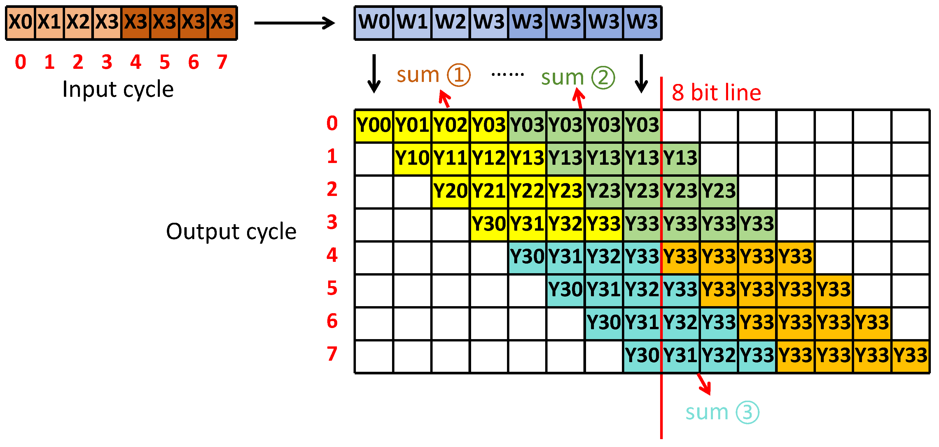
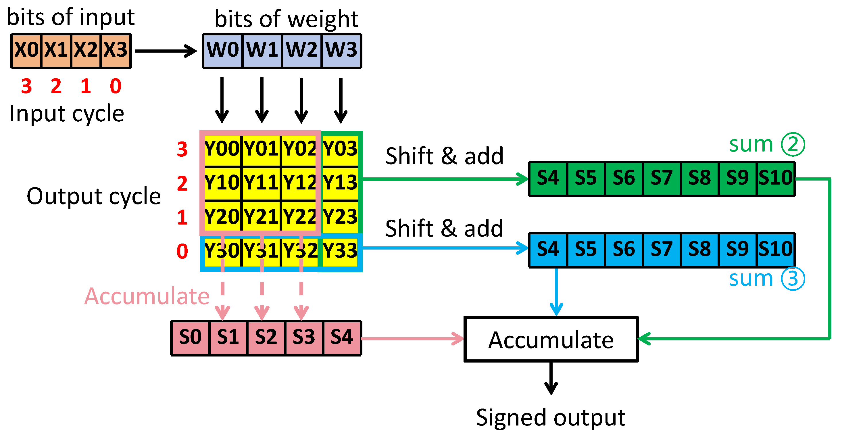
2.1. Improved Input-Side Parallel Mapping Strategy

Figure 2a illustrates the mapping strategy of ISP. Unlike the common SBIPW mapping strategy, ISP places the different significant bits of weight data on the same bit line rather than on the same word line, with each word line representing the same significant bit of all weight data. This method effectively transforms part of the column requirement of the weight matrix into a row requirement, making it more suitable for convolution kernels that have fewer input channels and more output channels. The timing for input data reception varies across word lines, with word lines representing higher significant bits receiving input data later. Although this increases the input cycle from four to seven, applying this method to appropriately sized convolution kernels can directly reduce the number of arrays occupied by the weight matrix or eliminate the remapping process, as shown on the right side of Figure 2b.
However, a notable limitation of ISP is that it only supports MAC operations for unsigned numbers. This is due to the sign bit calculations being spread across different cycles and mixed in with the unsigned results. This paper aims to tackle this issue at minimal cost.
Figure 3 illustrates the process of signed multiplication and accumulation in a CIM array using the ISP mapping strategy. Initially, the bit widths of the two operands are combined, resulting in a product bit width of eight. The operands are then sign-extended to ensure correct signed MAC operations, and an unsigned MAC is performed. Finally, the result is truncated to retain only the least significant eight bits. While this approach ensures correct results, it can excessively increase the area and computational latency due to unnecessary bit extension and truncation steps, underscoring the importance of optimizing operations for efficiency.
As shown on the top side of Figure 3, each column of the input matrix, which consists of data across varying cycles, corresponds to a significant bit in the final result. Consequently, data beyond the eighth column (A–G) are irrelevant to the computation, as they will be truncated later. The remaining matrix is further divided into three sections: the orange section represents the original input matrix, the green section corresponds to the additional bits introduced by the sign extension of the input data, and the blue section indicates the input data that compute with the sign-extended bits of the weight data.
The computation of the green section can be divided into two parts. The data from columns I to O can be directly mapped to the array, as these positions are already vacant in the ISP mapping strategy. Furthermore, since the input data in column H are identical to those in column I, the result for column H can be derived by shifting the result of column I, eliminating the need for additional input.
The input data in the blue section lack a clear pattern, which led to a revision of the rules for dividing the input matrix. As shown at the bottom of Figure 3, we have combined an additional set of data to form a new blue section. In this setup, each row in the blue section is identical to the data from the highest row in the orange section (row 5 in the matrix), along with the same associated weight data. Thus, the calculations for the blue section can be derived by shifting the results from the highest row of the orange section. Moreover, the computations for the additional data will ultimately be truncated, which does not affect the outcome. This approach allows the computation in the blue section to avoid using extra rows in the array or requiring additional input cycles.
Since the computation results from columns I to L require additional shifting and accumulation, we reversed the order of the input data, starting with the most significant bit and ending with the least significant bit. Figure 4 illustrates the data flow of the improved ISP mapping strategy. Input data and weight data are processed through the compute array to obtain the matrix–vector multiplication result Y, which is then accumulated by an ADC or an adder tree to produce the output S for each bit line. The first output S6 is shifted to obtain S7, which is then added back to the original output S to yield sum① and sum② shown in Figure 3. After outputting Y3, the data in the blue row are processed through shifting and summation to obtain sum③ in Figure 3, which is then added back to S to achieve the final output.
The cost of implementing this strategy includes the need for additional ADCs or adder trees, as well as an extra computation cycle. Figure 4 illustrates a multiplication operation involving just two data points. In an actual array, each column typically maps multiple weight data, each of which generates a Y matrix as shown. The blue rows in each Y matrix should first be summed together before performing shifting and subsequent operations. This process requires an additional small ADC or small adder tree. The specific size of these components is related to the bit width of the weight data. In the example shown, the weight data are four bits, meaning the required ADC or adder tree would be one-fourth the size of the array’s components. The extra computation cycle arises from the accumulation operations performed on sum①, sum②, and sum③. Despite this, these costs result in a reduction of three-quarters in area or latency compared to unsigned operations. If the original ISP is forcibly applied to signed networks, the data would be split into positive and negative parts for separate computations, leading to an area efficiency that is only one-fourth that of signed operations.

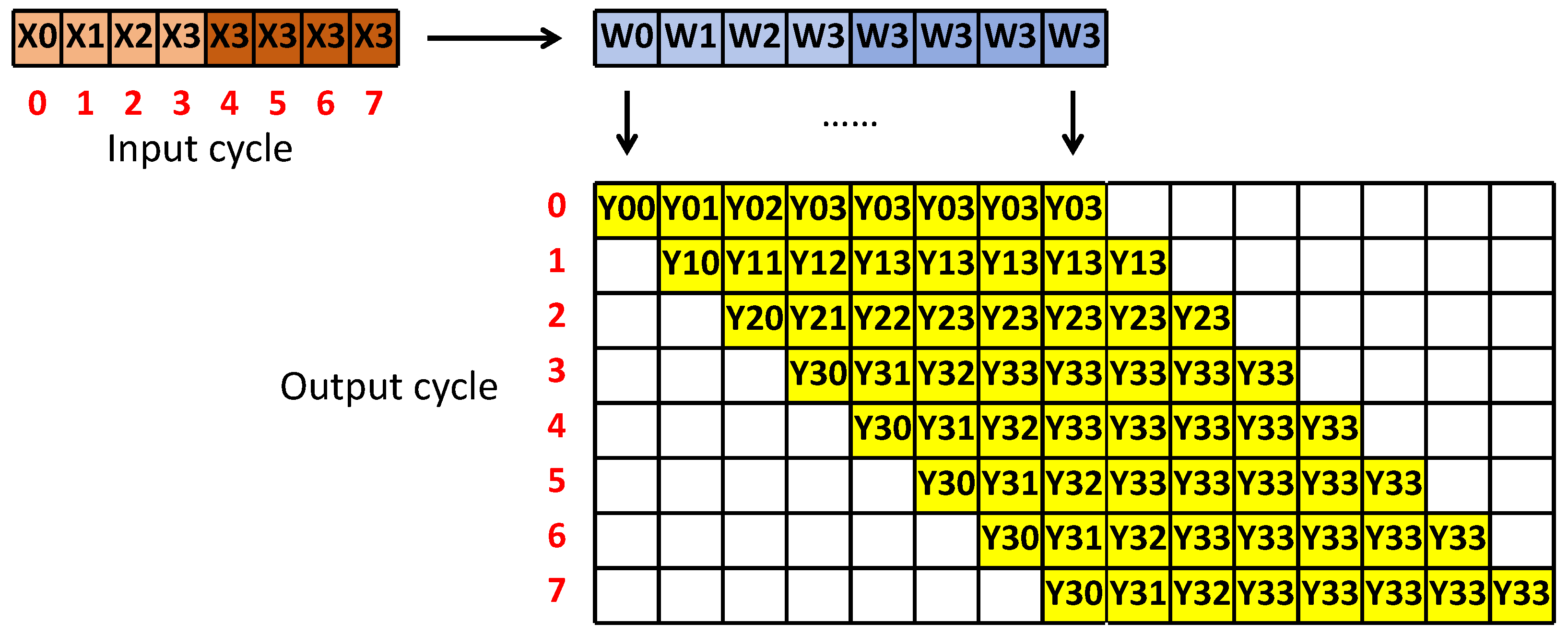
2.2. Improved Input- and Output-Side Parallel Mapping Strategy

By swapping the input vector and weight matrix in the ISP strategy, we obtain the IOSP mapping strategy and data flow, as shown in Figure 5. Compared to ISP, the IOSP significantly reduces the required computation cycles, completing all input data transfers in just one cycle. However, this comes at the cost of increased area demand for the array. For example, an n-bit weight occupies a rectangular area of 1 × n in the SBIPW mapping strategy, while, in the IOSP strategy, it requires an area of w × ( n + w 1 ) , where w is the bit width of the input data. Therefore, the IOSP is best suited for convolution layers with a limited number of input and output channels.
The IOSP shares the same drawback as the ISP: it cannot directly handle signed operations. To address this issue, we use a method similar to the improvements made in the ISP. Figure 6 illustrates the computation of two signed integers after performing sign extension according to the IOSP strategy. We still divide the entire weight matrix into four sections: the purple section represents the original weight matrix, the yellow section indicates the parts that do not require computation, and the results for the green and blue sections are obtained by shifting the computation results from the purple section, following the same improvements as in the ISP.
Figure 7 presents the mapping strategy and data flow of the improved IOSP. Since the array must select different mapping strategies based on the actual size of the convolution layer, the data arrangement in IOSP is kept the same as in the ISP, such as the order of data input. This approach avoids the need for additional peripheral circuits, allowing us to use the same set of circuits to compute the final result after generating the output matrix Y.

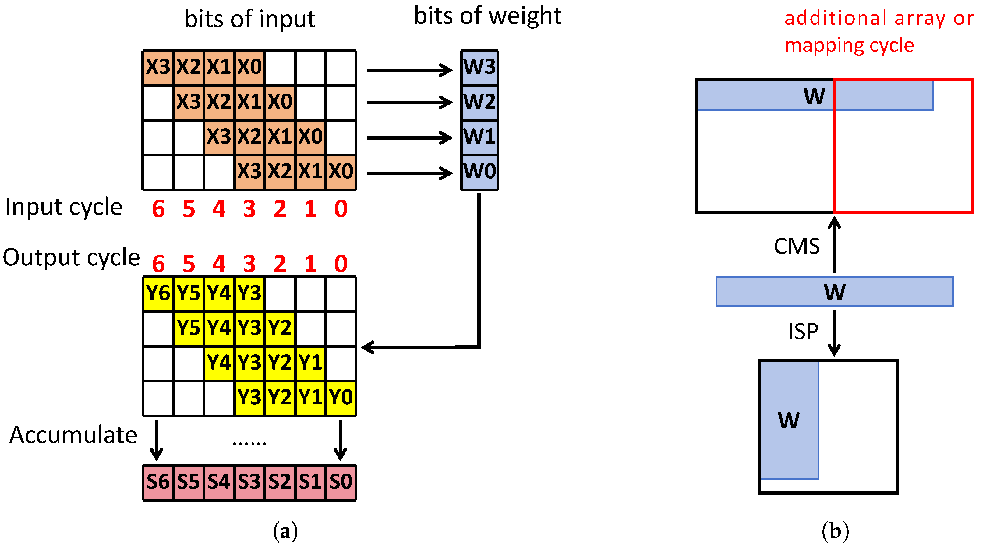
2.3. Improved Serial Bit Input Parallel Weight Mapping Strategy

In existing mapping strategies that use SBIPW or include weight duplication, prior research has managed to perform signed multiplication in CIM arrays by altering device circuits or employing other methods. This work, however, utilizes existing peripheral circuits to achieve the same functionality.
Figure 8 illustrates the computation process for signed numbers after width extension using the SBIPW mapping strategy. This approach divides the output matrix into four sections, with a partitioning method that differs slightly from ISP or IOSP. However, it still calculates the green and blue sections by shifting and accumulating the yellow partial products. Figure 9 shows the refined SBIPW mapping strategy and data flow. While it differs from ISP or IOSP, it continues to leverage the same peripheral circuits.

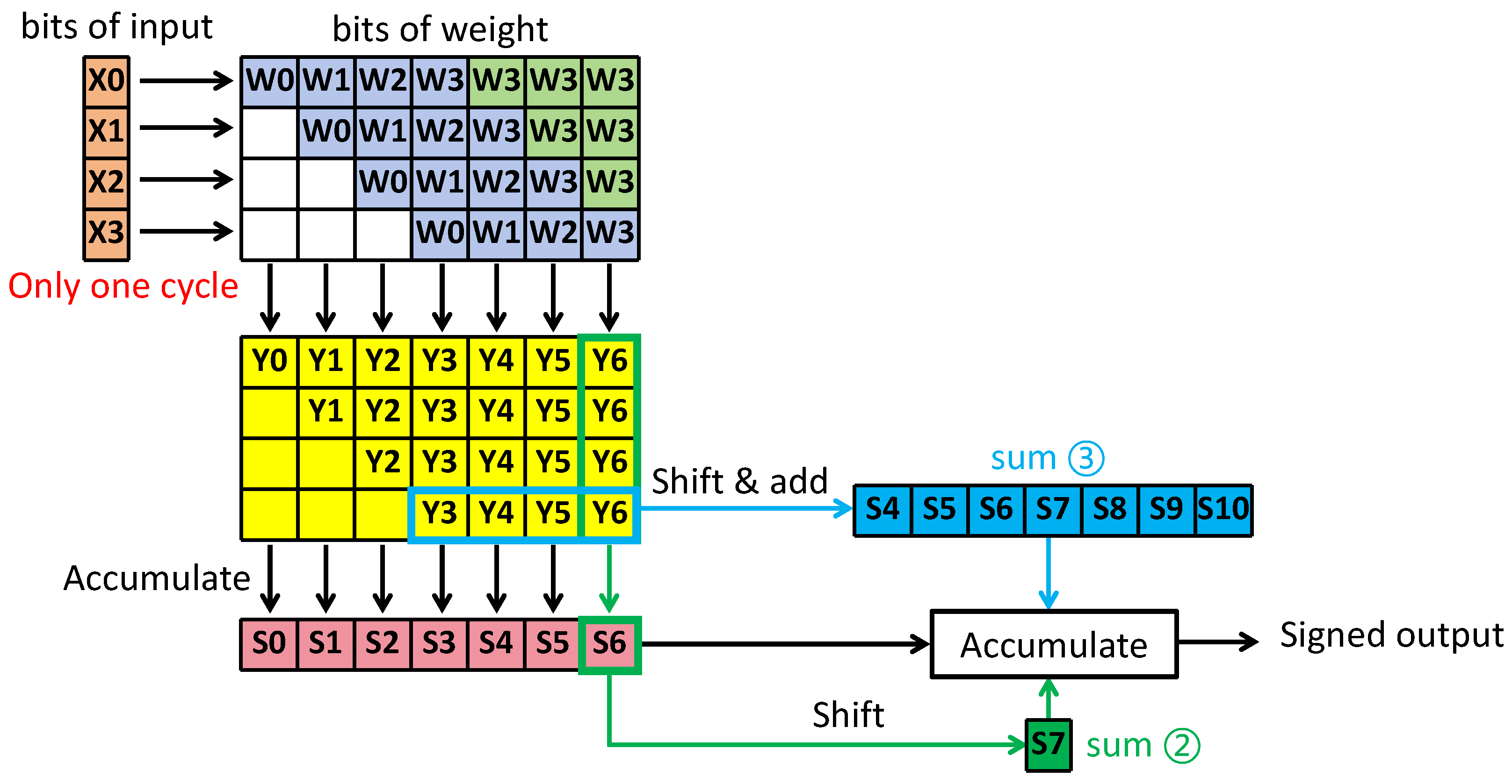
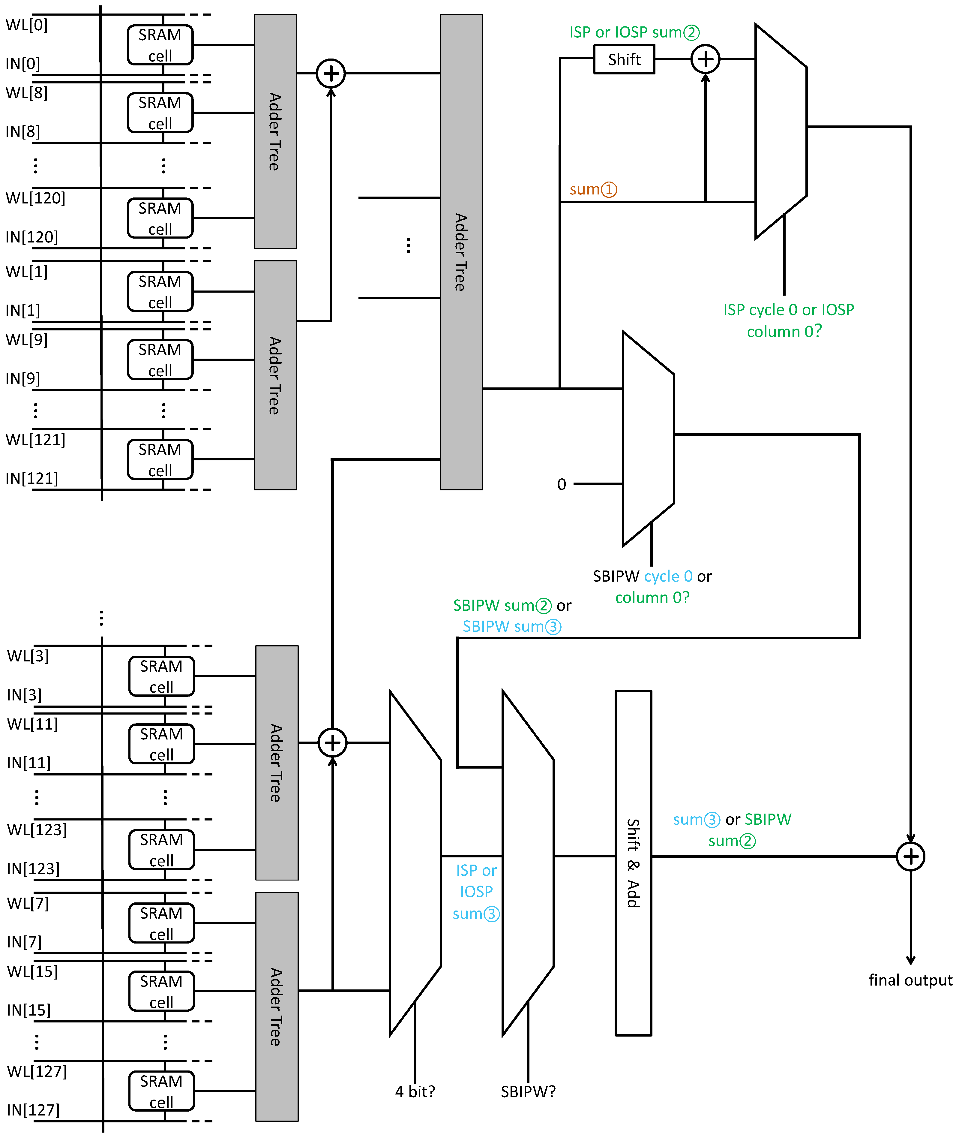
2.4. Improved Peripheral Circuits for Supporting Three Mapping Strategy

The circuit optimization and mapping strategy improvements outlined above can be applied to both digital and analog CIM architecture. We use DCIM as an example to illustrate the enhancement made to the peripheral circuit. As demonstrated in Figure 4, Figure 7 and Figure 9, the required additional computations can be categorized into three parts: shifting the result of a specific column and adding it directly to the original result, as in the sum② calculations in ISP and IOSP; shifting the sum of certain rows in a column, and then adding the shifted result to the original, as represented by sum③ in ISP and IOSP; shifting and accumulating the entire column’s result before adding it to the original output, as shown in sum② and sum③ in SBIPW. These three operations are controlled by three corresponding muxes in Figure 10.
The second type of computation requires summing the results of specific rows within the array. To facilitate this, we reordered the inputs to the adder tree, prioritizing the computation of rows with indices of 8n-1. Additionally, the mux following the computation checks the current data width. If the data width is four bits, the results from rows indexed as 8n-5 are also included in the final summation.
This circuit optimization requires only the integration of several muxes and shift adders around the existing adder tree, resulting in negligible overhead compared to the original peripheral circuitry. Even when performing unsigned operations, this setup ensures that almost no resources are wasted. More importantly, these circuits can be directly incorporated without modifying the existing array and device circuitry. This allows them to be combined with any adder tree design. If signed operations or support for multiple mapping strategies are unnecessary, the corresponding components can be easily removed, greatly enhancing the flexibility of the design.

3. Evaluation and Results

3.1. NeuroSim Introduction

Peng et al. introduced DNN+NeuroSim [17], an integrated framework developed in C++ with PyTorch/TensorFlow wrappers, designed to simulate the performance of DNN training and inference on compute-in-memory (CIM) architectures. It currently supports various architectures, including SRAM (where each cell stores one bit) and non-volatile memory (NVM) devices.
NeuroSim enables chip-level performance evaluation through simulations, providing key metrics such as chip area, latency, and both dynamic and static power consumption. With the PyTorch/TensorFlow wrappers, NeuroSim supports a multi-level and end-to-end simulation and design optimization framework, ranging from the device level (transistor sizes from 7 nm to 130 nm, eNVM device characteristics) to the circuit level (peripheral circuits, analog-to-digital converters, etc.), the chip level (tiles composed of multiple arrays, global interconnects, and buffers), and finally the algorithm level (various network topologies). This allows for precise inference accuracy evaluation and performance estimation.
Due to these advantages, NeuroSim has become a widely adopted fast simulation platform for CIM architectures in academia. Its open-source nature enables researchers to perform rapid preliminary evaluations of different CIM architectures, providing significant convenience in exploring novel hardware architectures, algorithm optimization, and energy efficiency improvements.

3.2. Evaluation Configuration

We utilized and further enhanced the latest version of NeuroSim V1.4, a simulation framework supporting digital CIM architectures. The array size was set to 128 × 128, with both activation and weight quantized to eight bits. All tests were conducted under the 22 nm technology node. We applied the enhanced circuit and mapping strategies to different networks for testing and compared the results with the baseline [8]. It is important to note that the bit-level mapping strategy can be integrated with the most commonly used weight mapping strategies, so we focused on comparing it with the baseline.

3.3. Results and Discussion

Since the VGG8 network typically uses ReLU as its activation function, we performed a separate simulation exclusively on the first layer. Table 1 presents the results of applying different mapping strategies to a layer with a convolution kernel size of 3 × 3 × 3 × 128. It is evident that, among the original three mapping strategies, SBIPW demonstrates the best performance, as both ISP and IOSP do not support signed weights, which limits their effectiveness. After applying our method, the performance of all three strategies saw significant improvements, with ISP benefiting the most due to the convolution kernel’s small input channel count and large output channel count. The energy efficiency increased to 4×, the speed improved to 2.67×, and the area was reduced to 51.6%. However, IOSP’s area efficiency remains significantly lower than that of the other two methods.
All simulations were performed on a high-performance computing system with the following configuration: dual AMD EPYC 7742 processors, 768 GB RAM memory, a Gigabyte MZ72-HB0 motherboard, and the Ubuntu operating system. This configuration ensured efficient execution of the simulations and accurate evaluation of the proposed strategies.
Table 2 presents the results for a convolution kernel of size 3 × 3 × 3 × 3. It is clear that the modified IOSP method is the most suitable for this kernel, which aligns with our expectations, achieving increases in energy efficiency and speed to 3.59× and 1.5×, respectively. As for ISP, its inability to effectively utilize idle arrays leads to a markedly reduced area efficiency compared to the other approaches.
Figure 11 illustrates the performance of forward inference on Yolov3-tiny and a modified version of Resnet18 under the condition that all three mapping strategies are used in combination. To determine the appropriate application of ISP and IOSP, we employ a conditional selection strategy based on their distinct advantages and limitations. Specifically, ISP is adopted when its implementation leads to a reduction in the number of arrays occupied by convolutional kernels, as illustrated in Figure 2b. Conversely, IOSP is applied only when it does not increase the array utilization of convolutional kernels. In all other cases, SBIPW is utilized as the default method. This selective approach ensures optimal resource efficiency while leveraging the strengths of each method.
We employed a variant of Resnet18, which uses the leaky ReLU activation function like Yolov3-tiny. As a result, the input matrix for each layer contains negative values. The results show that our method significantly outperforms the baseline in both latency and energy efficiency. Specifically, energy efficiency improved by 68.4% and 87.9%, while inference speed increased by 56.2% and 60.6%, respectively, all with less than a 1% increase in area.
Figure 11 also presents the comparison results under the condition of no area limitations, where the baseline uses twice the number of arrays as our method, with half of the input data being positive and the other half negative. Although the computational speed of the baseline is nearly equivalent to our method, the doubled array count also means that twice the input and output data need to be transferred, along with the extra overhead of accumulating the large matrix outputs. As a result, even with nearly 80% more area, our method still surpasses the baseline in both inference speed and energy efficiency.
Table 3 presents the performance of the large-scale Yolov3 network across different technology nodes. From the data in the table, two key conclusions can be drawn. First, our improved bit-level mapping strategy demonstrates consistent effectiveness across all technology nodes, with its performance being independent of the node variations. Specifically, compared to the baseline methods under all three technology nodes, our method achieves an average improvement of 60.70% in inference speed, a 91.03% increase in energy efficiency, and a minimal area overhead of less than 1%. Second, when analyzed alongside Figure 11, Table 3 further illustrates that our enhanced approach is effective across networks of varying scales. In practice, since the majority of layers in convolutional networks utilize large kernels, the bit-level mapping strategy applied to most layers (except for the first two and the last layer) is SBIPW. As a result, the overall performance of the network, which combines all three methods, closely aligns with the single-layer performance of SBIPW, demonstrating its efficiency and reliability as a core component of our approach.
However, this does not imply that our improvements to ISP and IOSP are of limited utility. The first two layers of a network typically feature large input feature maps, which require significant data transfer to the CIM arrays. As a result, these layers often occupy a small area but contribute substantially to the overall inference time. To address this, conventional CIM accelerators often replicate the weights of these layers multiple times to enable parallel computation, which incurs additional area overhead. Our enhanced methods effectively mitigate both the area and latency burdens by reducing the overhead associated with sign operations in these layers. In the Yolov3 network, the inference latency of the first two layers accounts for 15% of the total latency with the baseline methods, while, in the Yolov3-tiny network, this proportion rises to 20%. By applying our improved ISP and IOSP methods, we reduce the latency of these layers to just one-fourth of their original values, effectively addressing the bottleneck in the initial layers and contributing substantially to the overall efficiency improvements.
It should be emphasized that our method is universally applicable to any convolutional network involving signed computations when mapped to a CIM array, as the bit-level mapping strategy is architecture-agnostic. As discussed in Section 2.4, the optimized peripheral circuits are modular and compatible with any adder tree or ADC, regardless of the CIM architecture (analog or digital) or device technology. In this work, we focus on digital architectures for demonstration and experimental validation.

4. Conclusions

This work proposes an enhanced bit-level mapping and data flow strategy for SRAM-based CIM architectures, specifically addressing two critical limitations of existing approaches: insufficient support for signed computations and a lack of flexibility in practical applications. By introducing modifications to the ISP and IOSP mapping strategies and refining the adder tree and shift–add circuits, we were able to achieve significant improvements in both latency and area efficiency while maintaining minimal hardware overhead. Using NeuroSim V1.4, our improved ISP and IOSP demonstrated 4× and 3.59× improvements in energy efficiency for single-layer networks, respectively. Applied to larger models like Yolov3-tiny, the combined use of the three strategies achieved a 68.4% increase in energy efficiency and a 56.2% speedup, showcasing its effectiveness for neural network accelerators.
The main advantage of this work lies in the ability to support signed operations for the three bit-level mapping strategies using minimal, flexible, and easily reconfigurable peripheral circuit improvements. This approach significantly reduces application costs while enhancing versatility. These advancements are particularly promising for edge AI devices, real-time image processing systems, and low-power neural network accelerators, where efficient signed computation and flexibility are critical. However, one limitation of our approach is the parallel relationship between the bit-level mapping strategy and the data mapping strategy. While our improved bit-level mapping strategy is designed to be compatible with any data mapping strategy, potential conflicts could arise if other researchers’ enhancements to data mapping strategies involve adjustments to peripheral circuits. Future work will explore collaborative optimization methods to integrate both strategies effectively, with plans to further validate the proposed approach on FPGA-based platforms.

Author Contributions

Conceptualization, Z.C. and B.M.; formal analysis, H.C. and B.L.; methodology, F.L.; software, Q.C.; validation, Y.W.; writing—original draft, S.W.; writing—review and editing, S.W. All authors have read and agreed to the published version of the manuscript.

Funding

This research received no external funding.

Data Availability Statement

The data presented in this study are not publicly available due to confidentiality agreements and project restrictions. Access to the data may be granted under specific conditions, subject to approval by the project stakeholders. Requests for data access should be directed to y36958114@stu.xjtu.edu.cn.

Conflicts of Interest

Author Zhenjiao Chen was employed by the company The 58th Research Institute of China Electronics Technology Group Corporation. The remaining authors declare that the research was conducted in the absence of any commercial or financial relationships that could be construed as a potential conflict of interest.

Abbreviations

The following abbreviations are used in this manuscript:
CIMCompute-In-Memory
DCIMDigital Compute-In-Memory
CMSConventional Mapping Strategy
SBIPWSerial Bit Input Parallel Weight Mapping Strategy
ISPInput-Side Parallel Mapping Strategy
IOSPInput- and Output-Side Parallel Mapping Strategy
MACMultiply–Accumulate
ADCAnalog-to-Digital Converter
RAMRandom Access Memory

References

  1. Shafiee, A.; Nag, A.; Muralimanohar, N.; Balasubramonian, R.; Strachan, J.P.; Hu, M.; Williams, R.S.; Srikumar, V. ISAAC: A Convolutional Neural Network Accelerator with In-Situ Analog Arithmetic in Crossbars. In Proceedings of the 2016 ACM/IEEE 43rd Annual International Symposium on Computer Architecture (ISCA), Seoul, Republic of Korea, 18–22 June 2016; pp. 14–26. [Google Scholar] [CrossRef]
  2. Zhu, Z.; Lin, J.; Cheng, M.; Xia, L.; Sun, H.; Chen, X.; Wang, Y.; Yang, H. Mixed Size Crossbar based RRAM CNN Accelerator with Overlapped Mapping Method. In Proceedings of the 2018 IEEE/ACM International Conference on Computer-Aided Design (ICCAD), San Diego, CA, USA, 5–8 November 2018; pp. 1–8. [Google Scholar] [CrossRef]
  3. Zhang, Y.; He, G.; Wang, G.; Li, Y. Efficient and Robust RRAM-Based Convolutional Weight Mapping with Shifted and Duplicated Kernel. IEEE Trans.-Comput.-Aided Des. Integr. Circuits Syst. 2021, 40, 287–300. [Google Scholar] [CrossRef]
  4. Rhe, J.; Moon, S.; Ko, J.H. VW-SDK: Efficient Convolutional Weight Mapping Using Variable Windows for Processing-In-Memory Architectures. In Proceedings of the 2022 Design, Automation and Test in Europe Conference and Exhibition (DATE), Antwerp, Belgium, 14–23 March 2022; pp. 214–219. [Google Scholar] [CrossRef]
  5. Peng, X.; Liu, R.; Yu, S. Optimizing Weight Mapping and Data Flow for Convolutional Neural Networks on Processing-in-Memory Architectures. IEEE Trans. Circuits Syst. I Regul. Pap. 2020, 67, 1333–1343. [Google Scholar] [CrossRef]
  6. Qiao, X.; Cao, X.; Yang, H.; Song, L.; Li, H. AtomLayer: A Universal ReRAM-Based CNN Accelerator with Atomic Layer Computation. In Proceedings of the 2018 55th ACM/ESDA/IEEE Design Automation Conference (DAC), San Francisco, CA, USA, 24–28 June 2018; pp. 1–6. [Google Scholar] [CrossRef]
  7. Wang, S.; Liang, F.; Cao, Q.; Wang, Y.; Li, H.; Liang, J. A Weight Mapping Strategy for More Fully Exploiting Data in CIM-Based CNN Accelerator. IEEE Trans. Circuits Syst. II Express Briefs 2024, 71, 2324–2328. [Google Scholar] [CrossRef]
  8. Bai, Y.; Li, Y.; Zhang, H.; Jiang, A.; Du, Y.; Du, L. A Compilation Framework for SRAM Computing-in-Memory Systems with Optimized Weight Mapping and Error Correction. IEEE Trans.-Comput.-Aided Des. Integr. Circuits Syst. 2024, 43, 2379–2392. [Google Scholar] [CrossRef]
  9. Chen, Z.; Yu, Z.; Jin, Q.; He, Y.; Wang, J.; Lin, S.; Li, D.; Wang, Y.; Yang, K. CAP-RAM: A Charge-Domain In-Memory Computing 6T-SRAM for Accurate and Precision-Programmable CNN Inference. IEEE J.-Solid-State Circuits 2021, 56, 1924–1935. [Google Scholar] [CrossRef]
  10. He, Y.; Wang, Y.; Zhao, X.; Li, H.; Li, X. Towards State-Aware Computation in ReRAM Neural Networks. In Proceedings of the 2020 57th ACM/IEEE Design Automation Conference (DAC), San Francisco, CA, USA, 20–24 July 2020; pp. 1–6. [Google Scholar] [CrossRef]
  11. Jiang, H.; Huang, S.; Peng, X.; Su, J.W.; Chou, Y.C.; Huang, W.H.; Liu, T.W.; Liu, R.; Chang, M.F.; Yu, S. A Two-way SRAM Array based Accelerator for Deep Neural Network On-chip Training. In Proceedings of the 2020 57th ACM/IEEE Design Automation Conference (DAC), San Francisco, CA, USA, 20–24 July 2020; pp. 1–6. [Google Scholar] [CrossRef]
  12. Lu, L.; Tuan, D.A. A 47 TOPS/W 10T SRAM-Based Multi-Bit Signed CIM with Self-Adaptive Bias Voltage Generator for Edge Computing Applications. IEEE Trans. Circuits Syst. II Express Briefs 2023, 70, 3599–3603. [Google Scholar] [CrossRef]
  13. Choi, I.; Choi, E.J.; Yi, D.; Jung, Y.; Seong, H.; Jeon, H.; Kweon, S.J.; Chang, I.J.; Ha, S.; Je, M. An SRAM-Based Hybrid Computation-in-Memory Macro Using Current-Reused Differential CCO. IEEE J. Emerg. Sel. Top. Circuits Syst. 2022, 12, 536–546. [Google Scholar] [CrossRef]
  14. Jain, S.; Lin, L.; Alioto, M. ±CIM SRAM for Signed In-Memory Broad-Purpose Computing From DSP to Neural Processing. IEEE J.-Solid-State Circuits 2021, 56, 2981–2992. [Google Scholar] [CrossRef]
  15. You, H.; Li, W.; Shang, D.; Zhou, Y.; Qiao, S. A 1–8b Reconfigurable Digital SRAM Compute-in-Memory Macro for Processing Neural Networks. IEEE Trans. Circuits Syst. I Regul. Pap. 2024, 71, 1602–1614. [Google Scholar] [CrossRef]
  16. Lee, J.; Lu, A.; Li, W.; Yu, S. NeuroSim V1.4: Extending Technology Support for Digital Compute-in-Memory Toward 1 nm Node. IEEE Trans. Circuits Syst. I Regul. Pap. 2024, 71, 1733–1744. [Google Scholar] [CrossRef]
  17. Peng, X.; Huang, S.; Luo, Y.; Sun, X.; Yu, S. DNN+NeuroSim: An End-to-End Benchmarking Framework for Compute-in-Memory Accelerators with Versatile Device Technologies. In Proceedings of the 2019 IEEE International Electron Devices Meeting (IEDM), San Francisco, CA, USA, 7–11 December 2019; pp. 32.5.1–32.5.4. [Google Scholar] [CrossRef]
Figure 1. SBIPW calculation process diagram.
Electronics 14 01340 g001
Figure 2. (a) Schematic diagram of ISP data flow. (b) Advantages of ISP over CMS.
Electronics 14 01340 g002
Figure 3. Decomposition of signed MAC.
Electronics 14 01340 g003
Figure 4. Data flow of the improved ISP.
Electronics 14 01340 g004
Figure 5. Schematic diagram of IOSP data flow.
Electronics 14 01340 g005
Figure 6. Decomposition of signed weight matrix.
Electronics 14 01340 g006
Figure 7. Data flow of the improved IOSP.
Electronics 14 01340 g007
Figure 8. Decomposition of the signed output matrix.
Electronics 14 01340 g008
Figure 9. Data flow of the improved SBIPW.
Electronics 14 01340 g009
Figure 10. The schematic of the improved peripheral circuit.
Electronics 14 01340 g010
Figure 11. Performance of three methods on Yolov3-tiny and Resnet18.
Electronics 14 01340 g011
Table 1. Evaluation results on layer 3 × 3 × 3 × 128.
Mapping StrategyArea (mm2)Latency (us)TOPS/W
Baseline [8]SBIPW2.63756.402.047
ISP3.285106.401.211
IOSP6.14447.001.110
OursSBIPW1.83042.004.027
ISP1.69839.804.871
IOSP3.39945.604.643
Table 2. Evaluation results on layer 3 × 3 × 3 × 3.
Mapping StrategyArea (mm2)Latency (us)TOPS/W
Baseline [8]SBIPW1.33556.402.047
ISP3.28566.200.177
IOSP0.78015.641.177
OursSBIPW0.91542.004.027
ISP1.69834.200.436
IOSP0.78010.424.225
Table 3. Performance of the Yolov3 network across different technology nodes.
Technology Node22 nm10 nm7 nm
Baseline Ours Baseline Ours Baseline Ours
Area (mm2)156.78157.4343.9144.4621.7722.08
Latency (ms)168.44103.0698.2160.96280.0150.81
Energy Efficiency (TOPS/W)26.6951.2450.5696.2472.12137.58
Disclaimer/Publisher’s Note: The statements, opinions and data contained in all publications are solely those of the individual author(s) and contributor(s) and not of MDPI and/or the editor(s). MDPI and/or the editor(s) disclaim responsibility for any injury to people or property resulting from any ideas, methods, instructions or products referred to in the content.

