Article

Surge Current Capability and Failure Modes of 650 V p-GaN Gate HEMTs: A Multiphysics Study on Thermal–Electrical Coupling Effects

1
School of Integrated Circuit Science and Engineering, University of Electronic Science and Technology of China (UESTC), Chengdu 611731, China
2
Institute of Electronic and Information Engineering, University of Electronic Science and Technology of China (UESTC), Dongguan 523808, China
*
Author to whom correspondence should be addressed.
Electronics 2025, 14(7), 1321; https://doi.org/10.3390/electronics14071321
Submission received: 13 February 2025 / Revised: 20 March 2025 / Accepted: 25 March 2025 / Published: 27 March 2025
(This article belongs to the Special Issue Advances in Pulsed-Power and High-Power Electronics)

Abstract

:
In this study, we present a comprehensive comparative analysis of the surge current capability in the third quadrant for four commercial 650 V p-GaN gate HEMTs. Temperature-dependent experiments reveal varying degrees of negative correlation between surge current capability and device junction temperature across the four devices. Gate leakage testing and the decapsulation of failed devices identified two distinct failure modes. Through failure analysis techniques and TCAD simulations, the characteristics of these failure modes were thoroughly revealed. For Failure Mode I, the combined impact of electrical and thermal stress during the surge current process leads to extensive damage in the upper interconnect metal layer. For Failure Mode II, degradation of the metal to p-GaN Schottky contact under a strong electric field causes a rapid increase in the gate current, and the high gate current, coupled with the strong electric field, results in severe electromigration of the gate metal. Among the four tested devices, those exhibiting higher surge energy are more prone to gate damage, making them more susceptible to Failure Mode II.

1. Introduction

Due to the excellent electrical properties, including high electron mobility and high breakdown voltage, gallium nitride (GaN) high-electron-mobility transistors (HEMTs) have become a promising competitor in power electronics, featuring high frequency and superior power efficiency [1,2]. Despite the numerous advantages of GaN HEMTs, their reliability remains a critical factor that limits their wide application, including threshold voltage (VTH) instability [3,4], dynamic ON-resistance [5,6], and gate degradation under high-field stress [7,8]. The in-depth investigation of associated reliability mechanisms of GaN HEMTs will contribute to broadening the application scenarios. In practical applications, surge current capability is another critical reliability determinant for GaN HEMTs. For example, in bidirectional DC-DC converters or half-bridge switching circuits, the commonly adopted solution is to utilize the inherent bidirectional conduction characteristic of GaN HEMTs to achieve the freewheeling function in circuits. When the device operates in the third quadrant, under conditions of current overshoot/oscillation, it will be subjected to significant surge currents, potentially leading to device degradation or even failure. In particular, due to their superior device characteristics, GaN-based devices may face high-switching-frequency environments, where rapid switching transients under high dv/dt conditions are more likely to induce severe current overshoot and/or oscillations. Therefore, investigating the surge current capability of GaN HEMTs is a crucial research direction.
In contrast, SiC MOSFETs demonstrate superior intrinsic surge resistance capability under both single-pulse and repeated-pulse conditions due to its vertical structure and high thermal conductivity [9,10]. However, the surge current endurance of GaN HEMTs exhibits more pronounced thermal dependence. Therefore, research on the current surge capability of GaN HEMTs is of great significance. To date, research on surge current reliability has predominantly focused on GaN diodes [11], whereas studies on the surge current robustness of p-GaN gate HEMTs remain insufficient. Previous works [12,13] have studied the surge current capability of GaN HEMTs, particularly investigating the influence of the p-GaN contact on the device’s surge current characteristics. Additionally, the degradation of electrical parameters under repetitive surge current stress has also been reported [14], demonstrating the moderate deterioration (<20%) of threshold voltage (VTH), ON-resistance (RON), and drain leakage current (IDSS), as opposed to the substantial degradation (>500%) in the gate leakage current (IGSS). And the performance variations are related to the competing mechanisms of electron and hole trapping effects. Subsequently, a surge current-induced gate failure mechanism was proposed [15,16], demonstrating the catastrophic burnout of a 650 V GaN HEMT rated for 30 A under a peak surge current (Ipeak) of 53 A. However, existing studies on failure modes under surge current stress primarily rely on the observation of failure spots, while the underlying mechanisms responsible for these visible failures have been scarcely reported. In particular, research on gate-related failure has been largely limited to TCAD simulations without the necessary experimental validation. Therefore, it is of great importance to conduct a comparative study on the surge current characteristics of different commercial 650 V p-GaN gate HEMTs and to perform an in-depth failure mechanism analysis. This will help us to uncover potential variations in failure modes and will provide a more comprehensive understanding of the impact of surge current stress on mainstream p-GaN gate HEMTs.
In this work, the surge current characteristics of 650 V high-voltage p-GaN gate HEMTs from four different vendors are studied and compared at 25 °C and 150 °C. The impact of temperature on the surge current capability of these devices is comprehensively investigated, offering valuable insights for surge current reliability research. More importantly, two distinct failure modes and their underlying mechanisms are thoroughly identified and revealed.

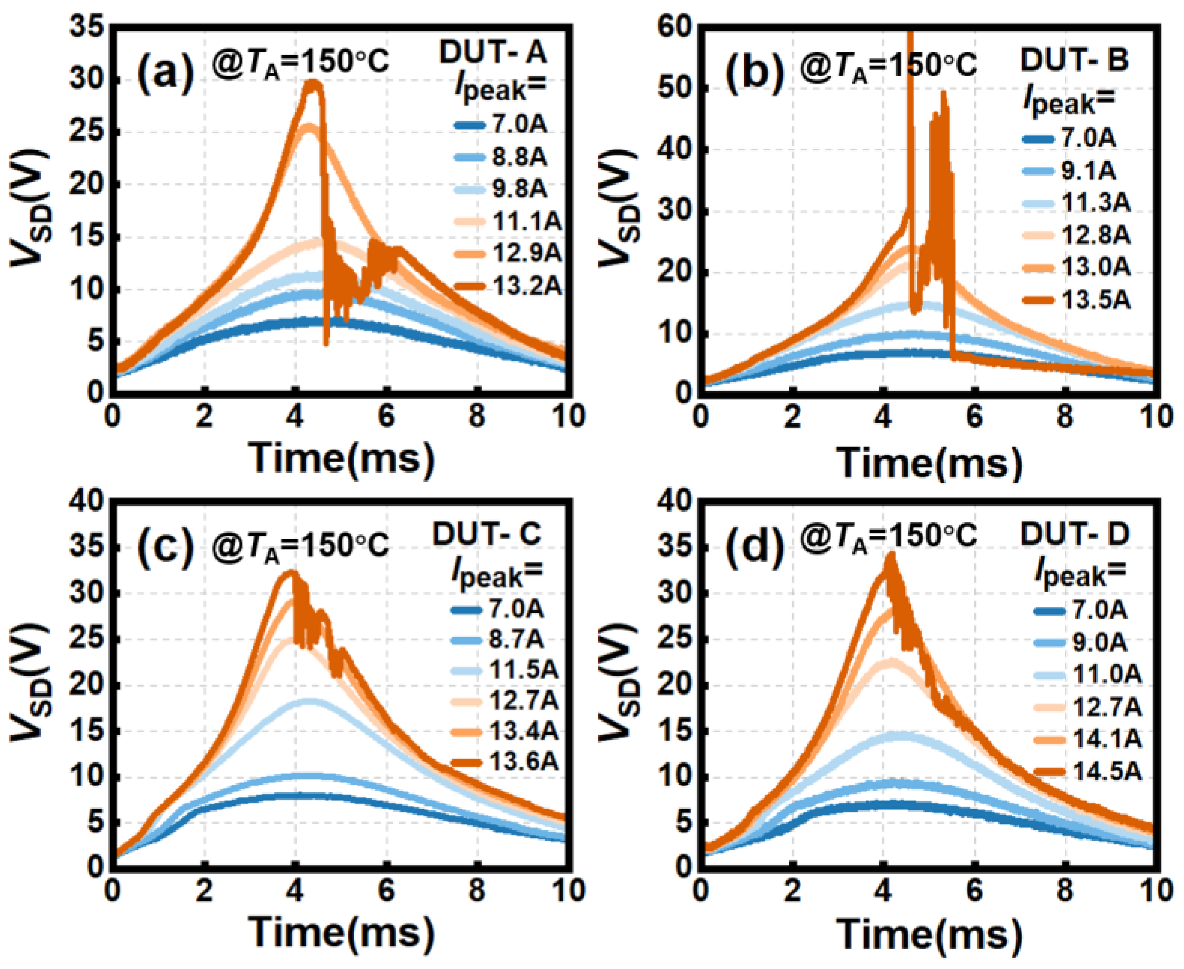
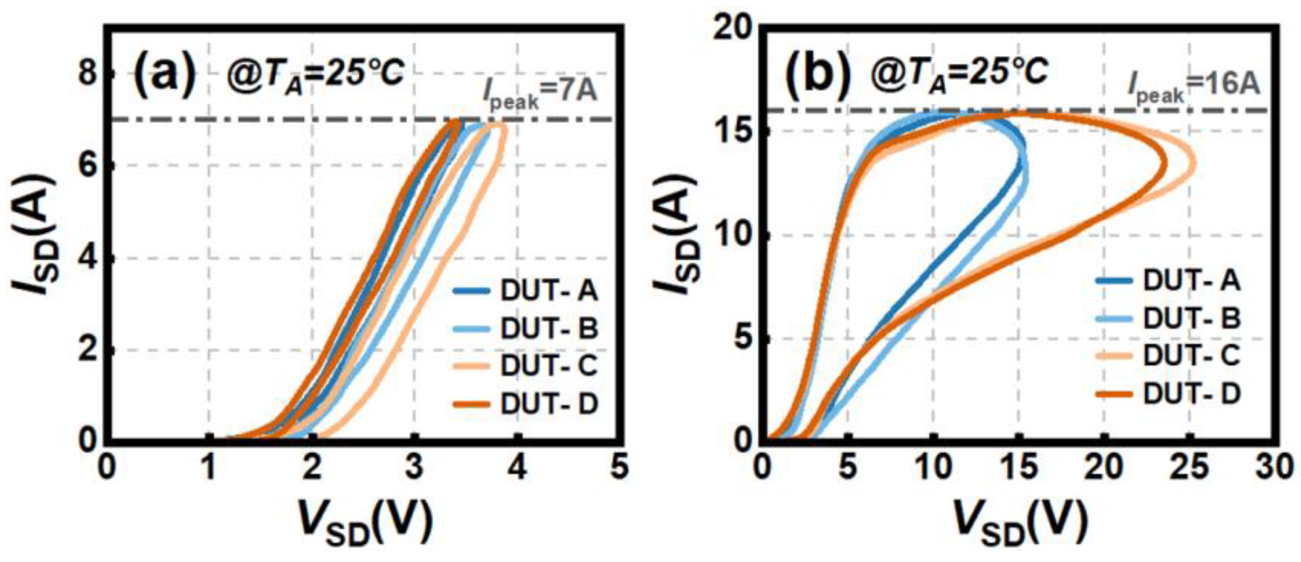
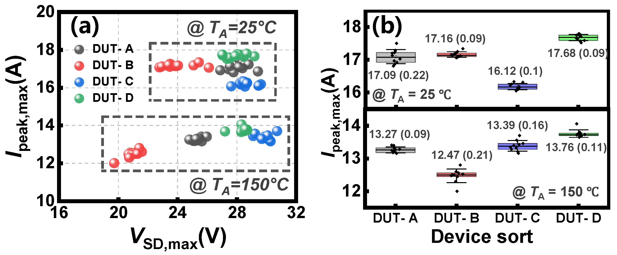
2. Surge Current Test and Results

Figure 1 presents the topology and platform of the surge current test circuit, which consists of a charging loop and a discharging loop. In the discharging loop, the surge current (Isurge) is generated following the LC oscillation principle. With an inductance of 5 mH and a capacitance of 2 mF, the circuit produces a half-sine surge current pulse of 10 ms. The peak surge current (Ipeak) depends on the charging voltage across the capacitor, as well as the capacitance and inductance values. By adjusting the operation timing of the charging and discharging loops, the Ipeak flowing through the device can be precisely modulated. This setup enables an in-depth investigation of the device’s surge current capability. The tested devices (DUTs) include four commercially available high-voltage GaN HEMTs [15,16,17,18], which share similar voltage and current ratings, ON-resistance, and Schottky p-GaN gates. Their key parameters are detailed in Table 1. DUT-A is GaN Systems (Ottawa, ON, Canada) GS-65-011-1-L. DUT-B is ROHM (Kyoto, Japan) GNP1150TCA-Z. DUT-C is Nexperia (Nijmegen, The Netherlands) GAN190-650EBE. DUT-D is Innoscience (Zhuhai, China) INN700DA190B.
During the experiment, the gate and source terminals of the device were intentionally shorted. As a half-sine surge current (ISD) flows from the source to the drain terminal, a corresponding voltage VSD (equivalent to VGD) develops between the source–gate and the drain terminal. Figure 2 presents the VSD versus time (VSD-t) characteristics under different Ipeak values at an ambient temperature (TA) of 25 °C. Clearly, the VSD of DUT-A~D exhibits an increasing trend as Ipeak rises, until reaching a critical Ipeak that leads to device failure. For DUT-A and DUT-B, a distinct slump in the VSD waveform marks the failure point. Prior to failure, Ipeak reaches 16.1–17.5 A, exceeding the nominal current rating by 40–59%. The static DC I–V measurements confirm short circuits among the gate, source, and drain terminals. In contrast, DUT-C and DUT-D do not exhibit an apparent VSD distortion. However, static I–V measurements reveal that their gate-to-drain terminals degrade into a resistor with kilo-ohm-level resistance, indicating device failure. These two distinct VSD-t waveform behaviors and the failure characteristics suggest the presence of two different failure modes in the DUTs.
To further study the impact of temperature on surge current capability, the surge current characteristics of the DUTs were measured at TA = 25, 75, 150, and 225 °C. Figure 3 plots the maximum VSD (i.e., VSD,max) and Ipeak values that each device can sustain without failure. It is observed that as temperature rises, Ipeak,max consistently decreases across all DUTs, indicating a reduction in surge current capability. The Ipeak,max represents the maximum surge current a device can endure without failure. Figure 4 presents the VSD versus time (VSD-t) characteristics under different Ipeak values at TA of 150 °C, in which the results align with the aforementioned conclusions.
Furthermore, a detailed comparison of surge current characteristics was conducted at TA = 25 °C and 150 °C. Figure 5a,b present the ISD-VSD curves of the DUTs under the Ipeak = 7 and 16 A at TA = 25 °C. At elevated peak currents (Ipeak = 16 A), all devices demonstrate pronounced current–voltage hysteresis induced by the surge-current-induced self-heating effect in the devices [12]. Notably, DUT-C and DUT-D show much larger hysteresis compared to DUT-A and DUT-B. The difference in the hysteresis loop may be attributed to differences in surge energy (Esurge), which can be presented as follows.
E s u r g e = 0 T ( I S D V S D ) d t
For Ipeak = 16 A, the Esurge quantities consumed in DUT-A and DUT-B are 0.879 and 0.91 J, respectively, while those for DUT-C and DUT-D are 1.143 and 1.079 J, respectively. The much higher Esurge quantity consumed in DUT-C and DUT-D leads to a severe self-heating effect, accelerating Ron degradation and thereby enlarging hysteresis. Crucially, under equivalent Ipeak conditions, DUT-C and DUT-D sustain higher VSD, while the gate terminal maintains a much higher voltage (e.g., ~10 V) than that in DUT-A and DUT-B. It is more susceptible to causing gate damage in DUT-C and DUT-D. At lower Ipeak values (i.e., 7 A), minimal hysteresis occurs as VSD,max aligns temporally with Ipeak, limiting thermal energy dissipation (i.e., Esurge < 0.2 J).
The ISD-VSD characteristics of the devices at 150 °C are shown in Figure 6. The Esurge values of DUT-A, DUT-B, DUT-C, and DUT-D at TA = 150 °C and Ipeak = 12.7 A are 0.855, 0.9, 1.115, and 1.063 J, respectively. With higher Esurge, DUT-C and DUT-D exhibit a more pronounced hysteresis loop. Additionally, under the same condition of Ipeak = 7 A, the hysteresis loop at 150 °C is larger than that at 25 °C, indicating that the surge current hysteresis behavior is temperature-sensitive.
As shown in Figure 7, 10 samples for each type of DUTs were measured to compare the surge current capability. It can be seen that even when featuring quite-similar current ratings (i.e., 11 or 11.5 A), the DUTs exhibit discernible difference in surge current capability.
The key performance of different DUTs subjected to surge pulses of sufficient magnitude (without inducing surge-related failure) are shown in Table 2. The analysis revealed that variations in VTH and RON remained statistically insignificant, making it challenging to identify the root causes of eventual degradation through these parameters. However, substantial discrepancies were observed in off-state gate leakage current IGSS. DUT-C and DUT-D exhibit significantly greater increases in IGSS, revealing that surge current can induce pronounced degradation effects within the gate region.
Furthermore, Figure 8 presents the post-failure gate leakage current (IGSS) characteristics of four device types under surge-induced failure at TA = 25 °C. All devices exhibited significantly increased IGSS following failure, though distinct failure signatures emerged in two characteristic groups. Similar to the VSD-t waveform observations, the detailed IGSS-VGS analysis reveals two different behaviors: DUT-A and DUT-B exhibit typical linear resistor-like characteristics; while DUT-C and DUT-D exhibit typical diode-like forward characteristics. Furthermore, as shown in Figure 9, post-characterization analysis through device decapsulation revealed distinct failure patterns: DUT-A and DUT-B exhibit conspicuous thermal damage marks consistent with catastrophic failure; whereas DUT-C and DUT-D maintain a clean surface morphology without visible defect signatures.
To explain the distinct failure characteristics observed above, comprehensive analytical investigations must be conducted to establish different failure models.

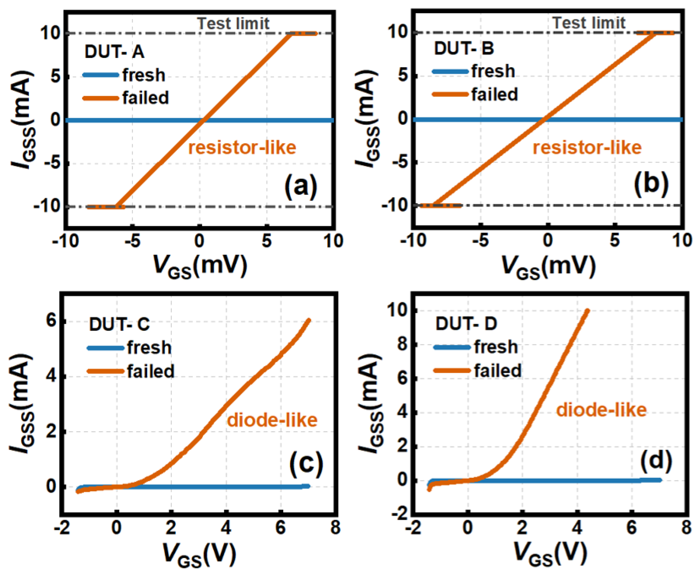
3. Device Failure Mode Analysis
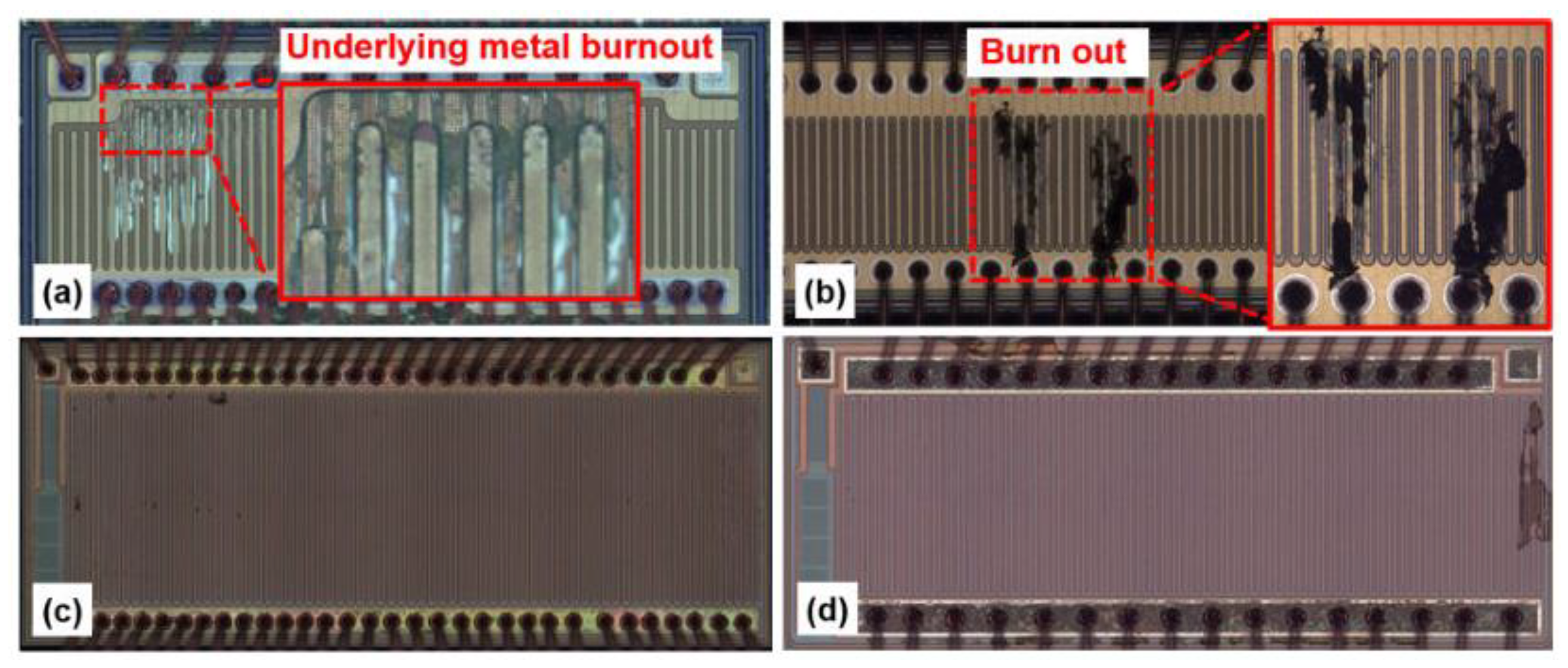
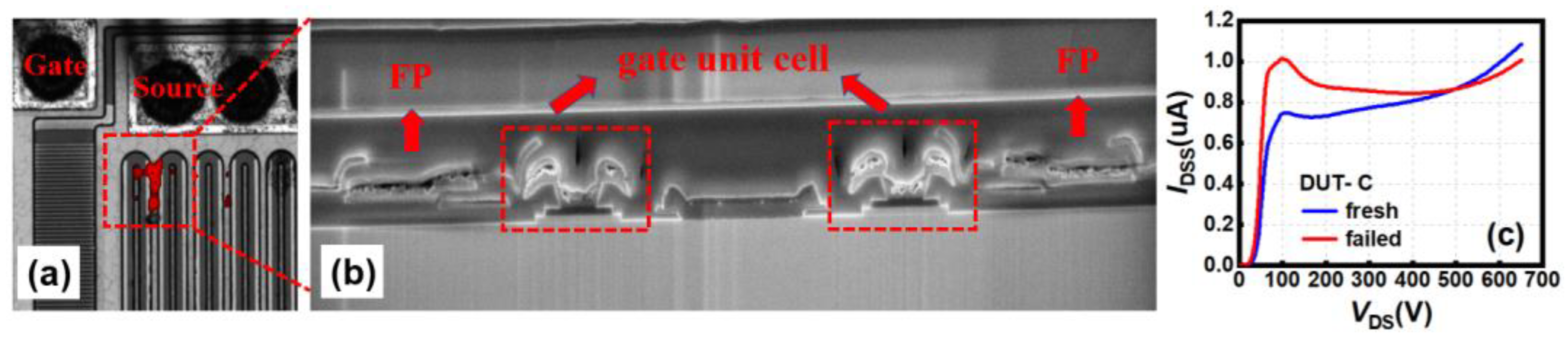
The experimental data reveal two distinct VSD-t waveform features correlated with gate leakage behavior and decapsulated chip observation. Correspondingly, two failure mechanisms manifest in the DUTs: DUT-A and DUT-B demonstrate Failure Mode I characteristics; whereas DUT-C and DUT-D exhibit Failure Mode II behavior.

3.1. Failure Mode I

As evidenced by Figure 9, DUT-A and DUT-B exhibit identical failure signatures, suggesting shared underlying failure mechanisms. DUT-A was selected for in-depth analysis as the representative case. The optical beam-induced resistance change (OBIRCH) technique precisely localized failure sites on the decapsulated device, as shown in Figure 10a. A distinctive green-light spot at the source finger location indicates localized resistance variations, confirming material structural degradation. As shown in Figure 10b, cross-sectional analysis via focused ion beam (FIB) and scanning electron microscopy (SEM) reveals pronounced thermal deformation in the upper interconnect metallization, particularly at source–drain terminals. The deformed interconnects demonstrate severe electromigration, forming source–drain bridging that correlates with the ohmic IDSS characteristics, as shown in Figure 10c.
Notably, the active region beneath the metallization remains a non-destructive structure, confirming that the failure mechanism originates from interconnect-level metal migration rather than epitaxial layer damage. It can be inferred that such a source–drain metal migration may also cause a short-circuit between the gate and source–drain terminals in the interconnect metal layer. Hence, as shown in Figure 8a,b, the gate leakage IGSS in DUT-A and DUT-B also show a resistor-like I–V curve. Such a source–drain interconnect metal failure is caused by the significantly high current and self-heating-induced thermal runaway during the current surge event.

3.2. Failure Mode II

As evidenced by Figure 9, DUT-C and DUT-D exhibit identical failure signatures, suggesting shared underlying failure mechanisms. DUT-C was selected for in-depth analysis as the representative case. As shown in Figure 11a, OBIRCH microscopy under VGD = 7 V bias conditions identifies failure localization through distinct red luminescence regions at both the source terminal finger and the underlying gate unit cell. As shown in Figure 11b, subsequent FIB-SEM cross-sectional analysis of the red-light spot reveals that the structural degradation patterns at the gate metal region may be related to this failure mode. To further verify the problems in the gate structure, Figure 12a,b provide analytical evidence via a TEM image coupled with EDS elemental analysis. It can be seen that metallic voids are formed in the gate metal stack as well as in the field plate (FP), particularly in the aluminum layer.
With degraded gate control, the diode-like forward gate leakage current characteristic is observed in Figure 8c,d. Apart from the damage to the gate metal, there are no other burn marks in the drain and source terminals or in the corresponding upper interconnect metal layers. Therefore, the IDSS of the device remains at a normal microampere level both before and after failure, as shown in Figure 11c.
To further investigate the underlying mechanisms of the failure mode, TCAD simulation was performed to analyze electric field distributions during surge current events. According to the surge current test results, the voltage VSD between the source and the gate (i.e., the source and the gate were connected together during the surge current test) and the drain of the device were significantly high during device failure. The simulation conditions, with critical VSD = 30 V (equivalent to VGD in this configuration), are close to the failure point. As shown in Figure 13a, electric field crowding occurs predominantly at the Schottky metal–p-GaN interface under surge stress. For Ipeak = 16.5 A, the peak electric field intensity reaches 3.24 MV/cm, which is close to the critical breakdown electric field of GaN. Figure 13b,c illustrate the current density distribution at the gate region and the electric field distribution along the Schottky metal–p-GaN interface at Ipeak = 10/15/20 A. With the increase in Ipeak, both the current density and the electric field intensity in the gate region exhibit an increasing trend. When the Ipeak rises from 15 to 20 A, the gate current exhibits a significant increase, while the peak electric field rapidly surpasses the critical electric field. This result shows consistency with the experimentally observed failure thresholds (Ipeak = 16~17 A).
Figure 14a illustrates the typical equivalent model of the Schottky type p-GaN gate. During third-quadrant surge conditions, the gate and source are shorted, and the surge current induces a high VSD (i.e., VGD). As shown in Figure 14b,c, when VGD > VGD,TH, the device enters the reverse conduction mode, and the equivalent Schottky barrier diode (SBD) is in a reverse blocking state. The failure initiates at the metal/p-GaN Schottky barrier interface (SBD) when depletion exceeds the critical extent. A high electric field forms at the metal/p-GaN interface, as shown in Figure 13, which is close to the critical breakdown field. Once this critical field is exceeded, breakdown occurs at the Schottky junction (SBD), leading to full forward conduction of the adjacent P-i-N diode, which is capable of resulting in a sharp increase in the gate current. The combination of the high gate current and electric field result in serve electromigration of aluminum metal [21], ultimately manifesting as discrete void formations within the gate metallization layer.

4. Conclusions

This study performs a comparative evaluation and a further in-depth investigation of the surge current capability of four different commercial 650 V p-GaN gate HEMTs. The self-heating effect induced by surge energy dissipation is identified as the dominant mechanism governing both surge response characteristics and surge current withstand capability. Through failure analysis of surge-induced degradation, two distinct failure mechanisms are revealed: Failure Mode I is a high-current- and self-heating-induced source–drain interconnect metal failure; Failure Mode II is a high-gate-current- and high-electric-field-induced electromigration of aluminum metal. The findings effectively bridge the critical gap between surface-level failure localization and comprehensive root-cause analysis in p-GaN gate HEMTs reliability research.

Author Contributions

Conceptualization, K.C. and R.P.; methodology, K.C., R.P. and S.H.; software, L.W.; validation, R.P., J.Z. and Q.Z.; investigation, K.C., R.P., S.H., J.Z., E.D. and Q.Z.; writing—original draft preparation, K.C. and R.P.; writing—review and editing, K.C. and R.P.; project administration, Q.Z. and B.Z. All authors have read and agreed to the published version of the manuscript.

Funding

This research was funded by the National Key Research and Development Program of China (grant numbers 2021YFB3600902 and 2021YFB3600903); by the National Natural Science Foundation of China (grant number: 62174019); and by the Guangdong Basic and Applied Basic Research Foundation (grant number: 2024A1515012139).

Data Availability Statement

The original contributions presented in this study are included in the article. Further inquiries can be directed to the corresponding author.

Conflicts of Interest

The authors declare no conflicts of interest.

References

  1. Chen, K.J.; Häberlen, O.; Lidow, A.; Tsai, C.L.; Ueda, T.; Uemoto, Y. GaN-on-Si Power Technology: Devices and Applications. IEEE Trans. Electron Device 2017, 64, 779–795. [Google Scholar] [CrossRef]
  2. Chow, T.P. Progress in high voltage SiC and GaN power switching devices. Mater. Sci. Forum 2014, 778–780, 1077–1082. [Google Scholar]
  3. Sayadi, L.; Iannaccone, G.; Sicre, S.; Häberlen, O.; Curatola, G. Threshold Voltage Instability in p-GaN Gate AlGaN/GaN HFETs. IEEE Trans. Electron Device 2018, 65, 2454–2460. [Google Scholar]
  4. He, J.; Tang, G.; Chen, K.J. VTH Instability of p-GaN Gate HEMTs Under Static and Dynamic Gate Stress. IEEE Electron Device Lett. 2018, 39, 1576–1579. [Google Scholar] [CrossRef]
  5. Wang, H.; Wei, J.; Xie, R.; Liu, C.; Tang, G.; Chen, K.J. Maximizing the Performance of 650-V p-GaN Gate HEMTs: Dynamic RON Characterization and Circuit Design Considerations. IEEE Trans. Power Electron. 2017, 32, 5539–5549. [Google Scholar] [CrossRef]
  6. Zhong, K.; Wei, J.; He, J.; Feng, S.; Wang, Y.; Yang, S.; Chen, K.J. IG- and VGS-Dependent Dynamic RON Characterization of Commercial High-Voltage p-GaN Gate Power HEMTs. IEEE Trans. Ind. Electron. 2022, 69, 8387–8395. [Google Scholar] [CrossRef]
  7. Bao, Q.; Yang, S.; Sheng, K. UIS Withstanding Capability of GaN E-HEMTs with Schottky and Ohmic p-GaN contact. In Proceedings of the International Symposium on Power Semiconductor Devices and ICs (ISPSD), Vienna, Austria, 13–18 September 2020. [Google Scholar]
  8. Li, S.; Liu, S.; Zhang, C.; Qian, L.; Ge, C.; Xin, S.; Sun, W.; Yang, Z.; Zhu, Y.; Ni, L. Understanding Electrical Parameter Degradations of P-GaN HEMT Under Repetitive Short-Circuit Stresses. IEEE Trans. Power Electron. 2021, 36, 12173–12176. [Google Scholar] [CrossRef]
  9. Li, H.; Wang, J.; Ren, N.; Xu, H. Investigation of 1200 V SiC MOSFETs’ Surge Reliability. Micromachines 2019, 10, 485. [Google Scholar] [CrossRef] [PubMed]
  10. Mihaila, A.; Liu, C.; Romano, G.; Bianda, E.; Wirths, S.; Arango, Y.; Knoll, L.; Baschnagel, A.; Boksteen, B. Surge current capability of 6.5kV-rated SiC MOSFETs. In Proceedings of the International Symposium on Power Semiconductor Devices and ICs (ISPSD), Vienna, Austria, 13–18 September 2020. [Google Scholar]
  11. Liu, J.; Zhang, R.; Xiao, M.; Pidaparthi, S.; Cui, H.; Edwards, A.; Baubutr, L.; Drowley, C.; Zhang, Y. Surge Current and Avalanche Ruggedness of 1.2-kV Vertical GaN p-n Diodes. IEEE Trans. Power Electron. 2021, 36, 10959–10964. [Google Scholar] [CrossRef]
  12. Liu, Y.; Yang, S.; Han, S.; Sheng, K. Investigation of Surge Current Capability of GaN E-HEMTs in The Third Quadrant: The Impact of P-GaN Contact. IEEE J. Emerg. Sel. Top. Power Electron. 2019, 7, 1465–1474. [Google Scholar]
  13. Liu, Y.; Han, S.; Yang, S.; Sheng, K. Surge Current Capability of GaN E-HEMTs in Reverse Conduction Mode. In Proceedings of the International Symposium on Power Semiconductor Devices and ICs (ISPSD), Shanghai, China, 19–23 May 2019. [Google Scholar]
  14. Wang, X.; Chen, W.; Sun, R.; Liu, C.; Xia, Y.; Xin, Y.; Xu, X.; Wang, F.; Chen, X.; Chen, Y.; et al. Degradation Behavior and Mechanism of GaN HEMTs with P-Type Gate in the Third Quadrant Under Repetitive Surge Current Stress. IEEE Trans. Electron Device 2022, 69, 5733–5741. [Google Scholar] [CrossRef]
  15. Wang, X.; Chen, W.; Sun, R.; Liu, C.; Chen, X.; Xia, Y.; Xu, X.; Wang, Z.; Luo, P.; Zhang, Y.; et al. Failure Behavior and Mechanism of p-GaN Gate AlGaN/GaN HEMTs in the Third Quadrant Under Repetitive Surge Current Stress. IEEE Trans. Electron Device 2024, 71, 1694–1701. [Google Scholar] [CrossRef]
  16. Wang, X.; Sun, R.; Xia, Y.; Liu, C.; Chen, X.; Chen, W.; Zhang, B. Gate Damage Mechanism of Schottky-Type p-GaN Gate HEMTs in Reverse Conduction Mode Under Surge Current Stress. In Proceedings of the International Symposium on Power Semiconductor Devices and ICs (ISPSD), Bremen, Germany, 2–6 June 2024. [Google Scholar]
  17. GS-065-011-1-L. Available online: https://gansystems.com/ (accessed on 1 November 2024).
  18. GNP1150TCA-Z. Available online: https://rohm.com/ (accessed on 1 November 2024).
  19. GAN190-650EBE. Available online: https://nexperia.com/ (accessed on 1 November 2024).
  20. INN700DA190B. Available online: https://innoscience.com/ (accessed on 1 November 2024).
  21. Black, J.R. Electromigration—A brief survey and some recent results. IEEE Trans. Electron Device 1969, 16, 338–347. [Google Scholar]
Figure 1. (a) The circuit topology, (b) test platform, and (c) DUTs of the surge current testing.
Electronics 14 01321 g001
Figure 2. Waveform of the VSD-t of the devices during the surge current test at TA = 25 °C: (a) DUT-A; (b) DUT-B; (c) DUT-C; (d) DUT-D.
Electronics 14 01321 g002
Figure 3. Waveform of the VSD,max-Ipeak of the devices at TA = 25/75/150/225 °C: (a) DUT-A; (b) DUT-B; (c) DUT-C; (d) DUT-D.
Electronics 14 01321 g003
Figure 4. Waveform of the VSD-t of the devices during surge current test at TA = 150 °C: (a) DUT-A; (b) DUT-B; (c) DUT-C; (d) DUT-D.
Electronics 14 01321 g004
Figure 5. ISD-VSD characteristics of the DUTs at TA = 25 °C under Ipeak of (a) 7 A and (b) 16 A.
Electronics 14 01321 g005
Figure 6. ISD-VSD characteristics of the DUTs at TA = 150 °C under Ipeak of (a) 7 A and (b) 12.7 A.
Electronics 14 01321 g006
Figure 7. (a) The statistical values of the Ipeak,max and VSD,max of the DUTs at TA = 25 °C and 150 °C without failure. Ten samples were tested for each type of DUT. (b) The Ipeak,max distributions across 10 samples of different devices, along with their mean (standard deviation) values.
Electronics 14 01321 g007
Figure 8. IGSS characteristics of the failed devices for (a) DUT-A, (b) DUT-B, (c) DUT-C, and (d) DUT-D.
Electronics 14 01321 g008
Figure 9. Decapsulation of failed devices for (a) DUT-A, (b) DUT-B, (c) DUT-C, and (d) DUT-D.
Electronics 14 01321 g009
Figure 10. (a) OBIRCH image of the failed device from DUT-A. (b) Cross-sectional FIB-SEM image of the failed device at green-light spot. (c) IDSS characteristics of the failed device from DUT-A.
Electronics 14 01321 g010
Figure 11. (a) OBIRCH image of the failed device from DUT-C. (b) Cross-sectional FIB-SEM image of the failed device at the red-light spot. (c) IDSS characteristics of the failed device from DUT-C.
Electronics 14 01321 g011
Figure 12. (a) TEM image of the gate structure of the failed device. (b) EDS elemental analysis result of gate metal.
Electronics 14 01321 g012
Figure 13. Electric field simulation results of DUT-C: (a) The overall distribution image under Ipeak = 16.5 A; VSD = VGD = 30 V. (b) The current density distribution at the gate region and (c) electric field distribution image at the cutline under Ipeak = 10/15/20 A; VSD = VGD = 30 V.
Electronics 14 01321 g013
Figure 14. (a) Equivalent model of the gate stack structure of p-GaN HEMT. The simulated energy band diagrams under (b) the initial state at VSD = VGD = 0 V and (c) surge current stress state at VSD = VGD = 30 V.
Electronics 14 01321 g014
Table 1. Key parameters of DUTs.
ParametersDUT-A [17]DUT-B [18]DUT-C [19]DUT-D [20]
Voltage Rating (V)650650650700
Current Rating (A)111111.511.5
Typical RDS_ON (mΩ)150150138138
p-GaN gate typeSchottkySchottkySchottkySchottky
Table 2. Key parameters of DUTs before and after surge pulse.
ParametersDUT-ADUT-BDUT-CDUT-D
VTH (V)1.44 (initial)1.5 (initial)1.7 (initial)1.61 (initial)
1.47 (16.9 A)1.51 (17.3 A)1.68 (17.2 A)1.34 (17.5 A)
RDS_ON (mΩ)179.3 (initial)201.2 (initial)196.4 (initial)198.1 (initial)
188.8 (16.9 A)220.6 (17.3 A)197.8 (17.2 A)186.2 (17.5 A)
IGSS (μA)41 (initial)76 (initial)75 (initial)44 (initial)
140 (16.9 A)99 (17.3 A)3500 (17.2 A)2070 (17.5 A)
Disclaimer/Publisher’s Note: The statements, opinions and data contained in all publications are solely those of the individual author(s) and contributor(s) and not of MDPI and/or the editor(s). MDPI and/or the editor(s) disclaim responsibility for any injury to people or property resulting from any ideas, methods, instructions or products referred to in the content.

