

Optimizing the Efficiency of Series Resonant Half-Bridge Inverters for Induction Heating Applications


Abstract
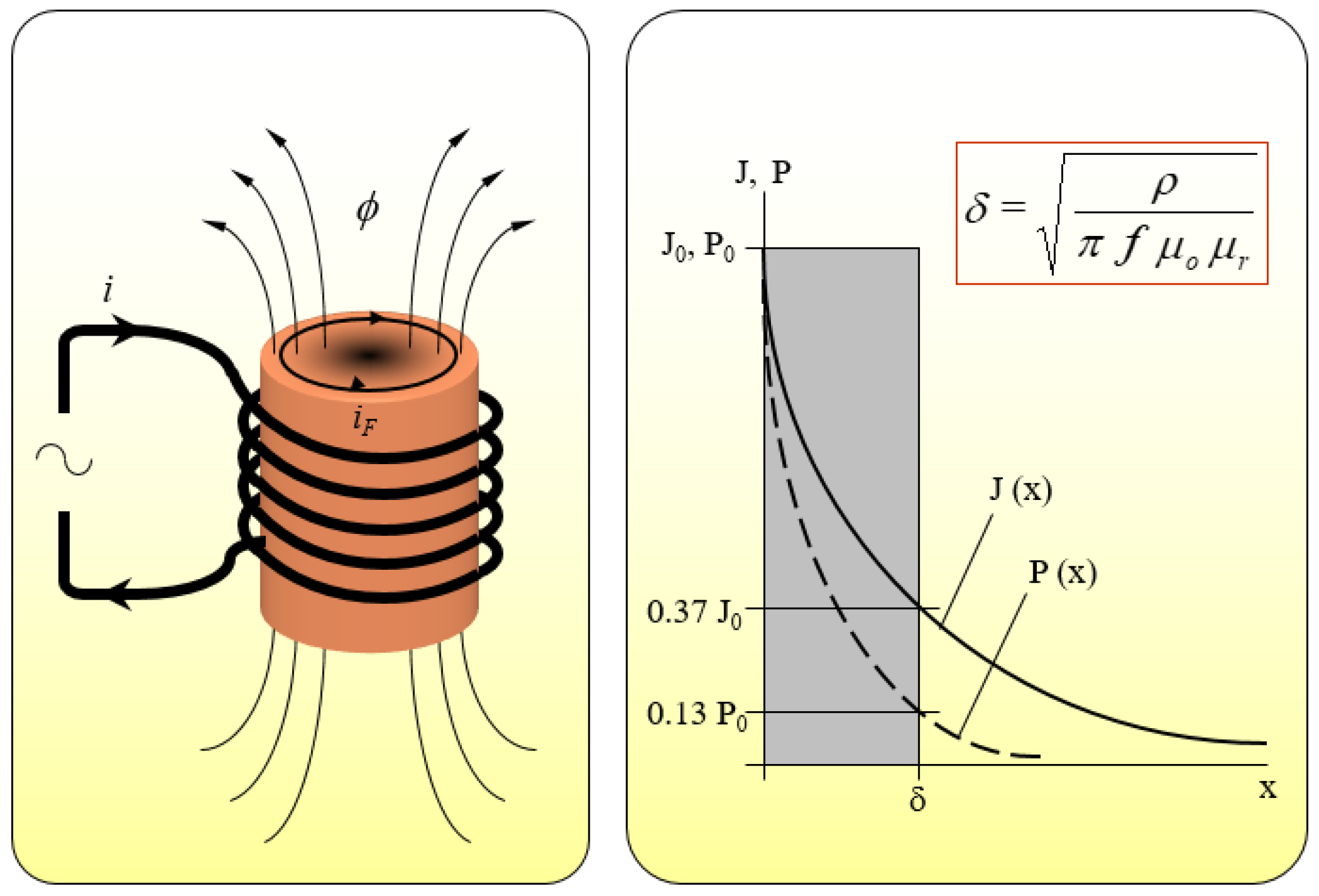
1. Introduction
2. Materials and Methods
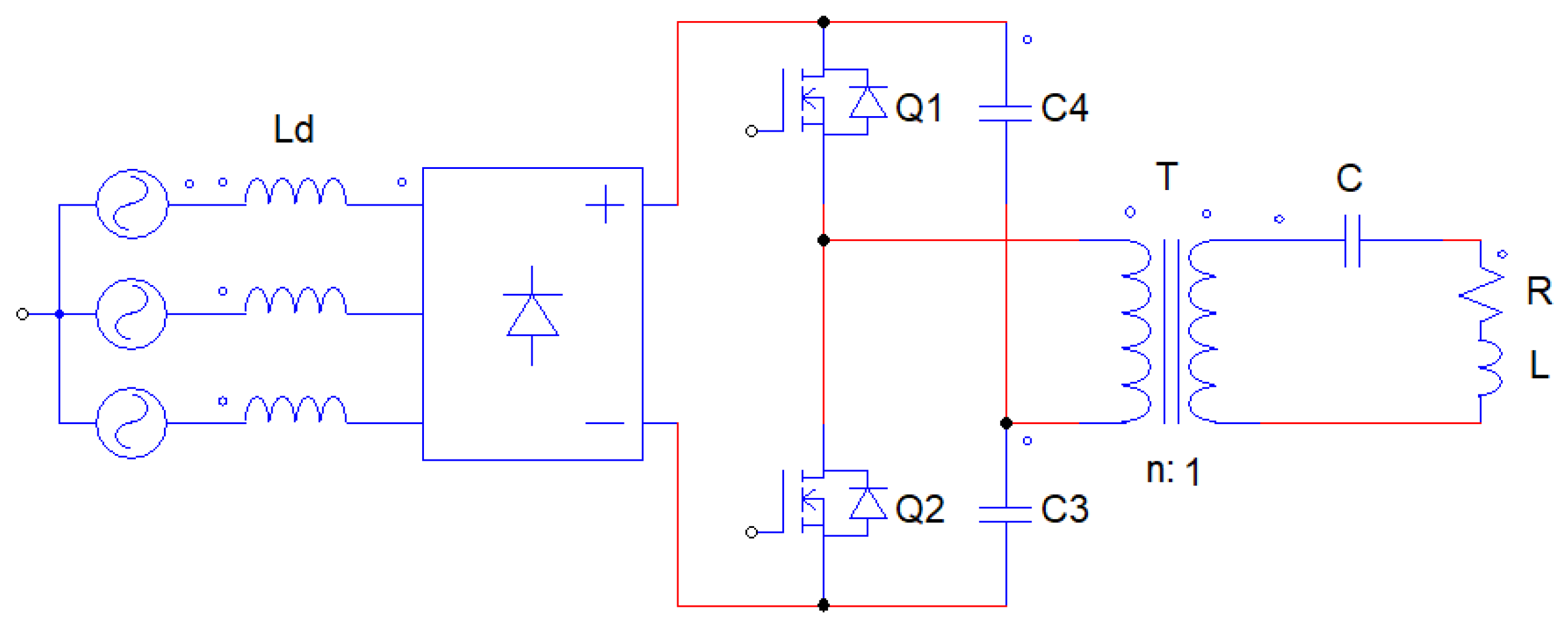
2.1. Converter Configuration
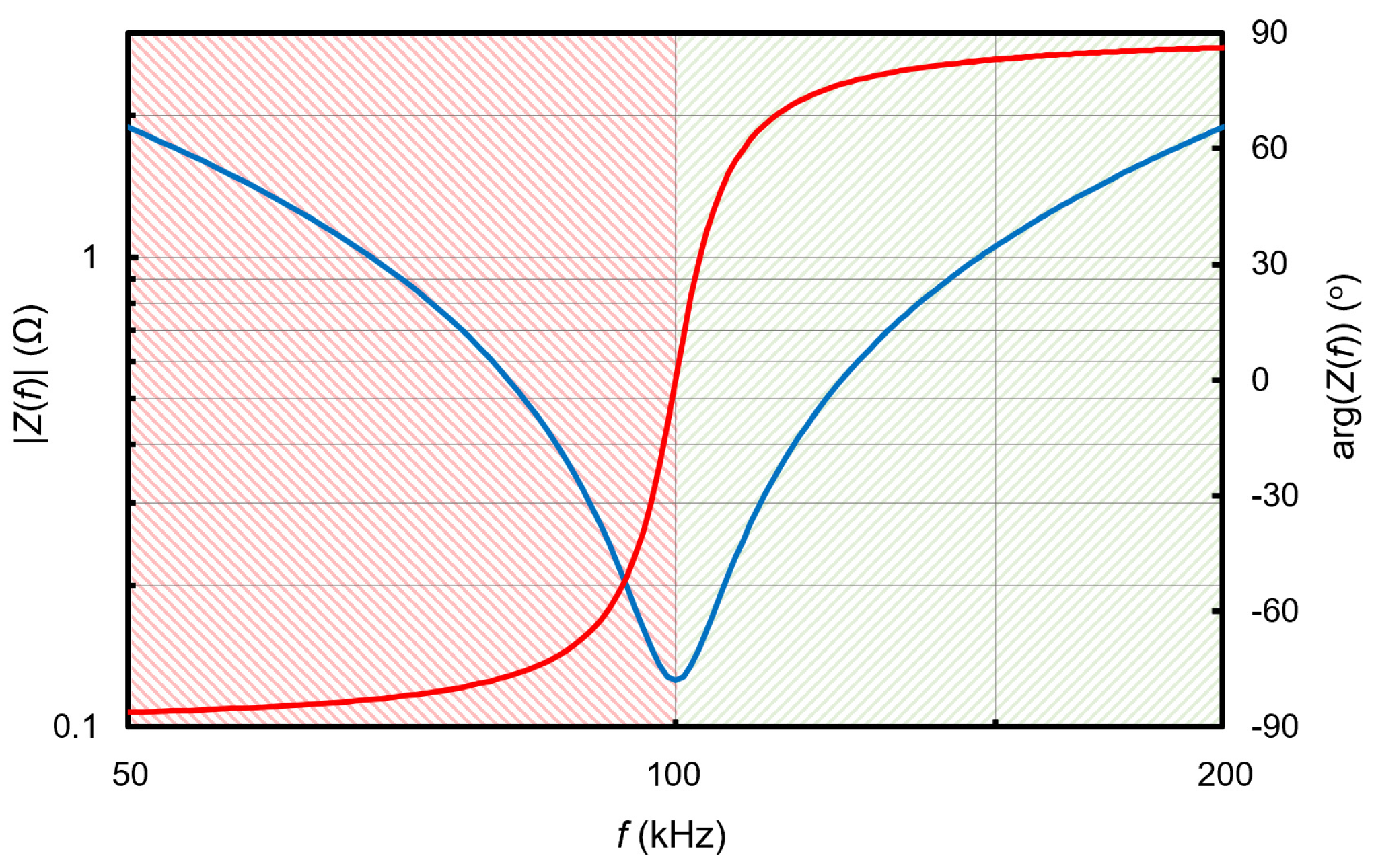
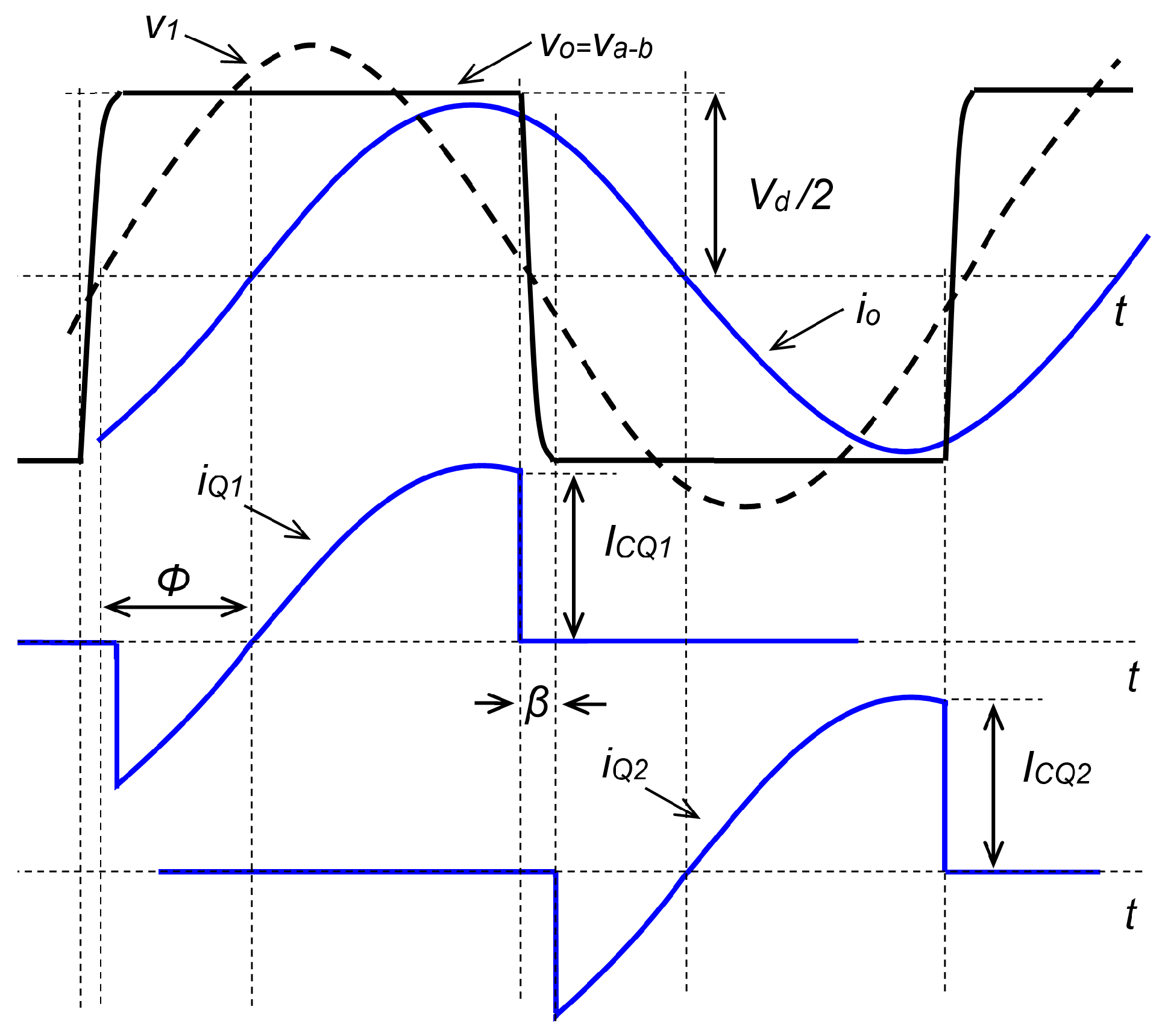
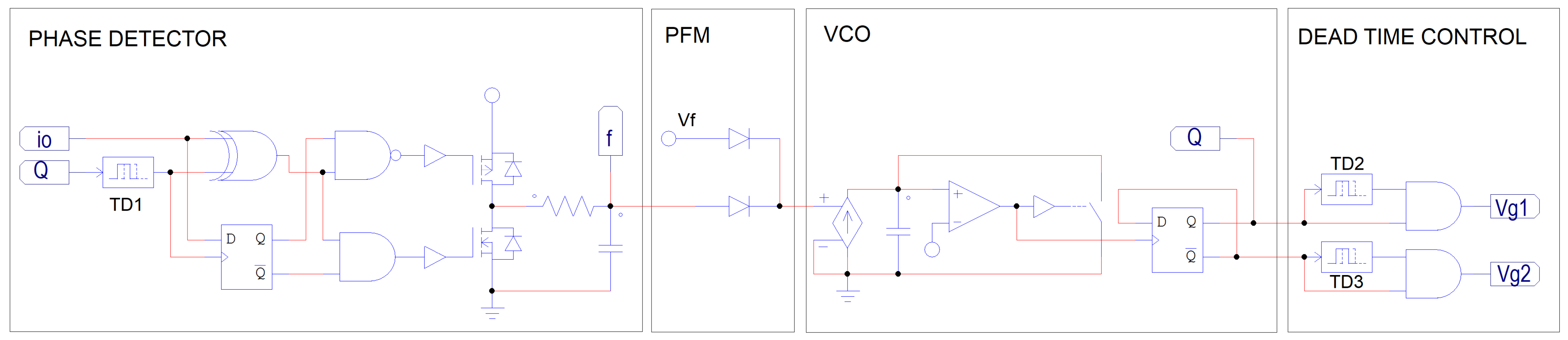
2.2. Control by Pulse Frequency Modulation (PFM)
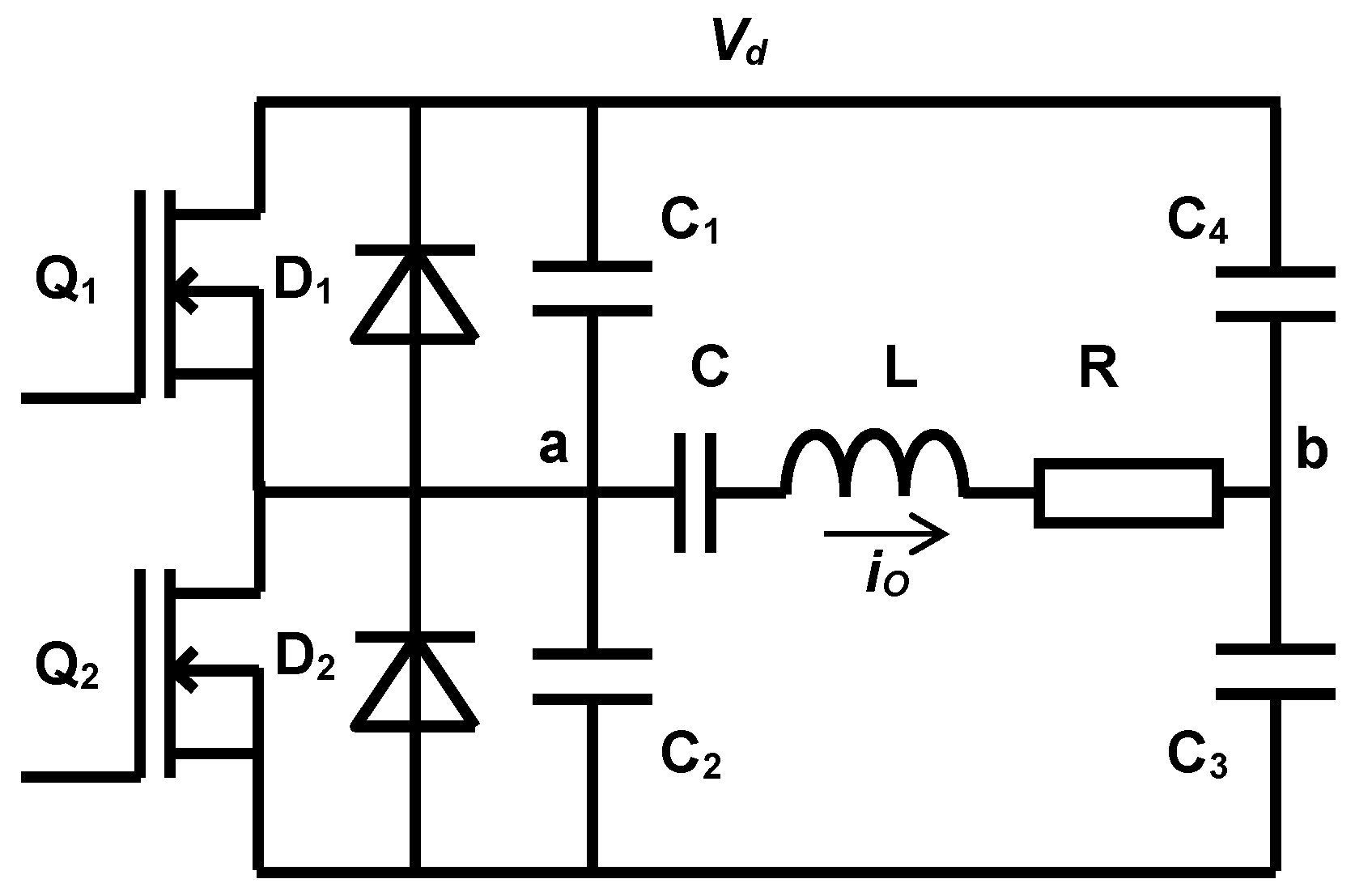
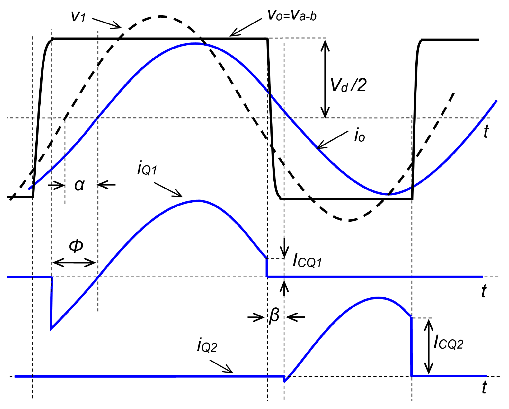
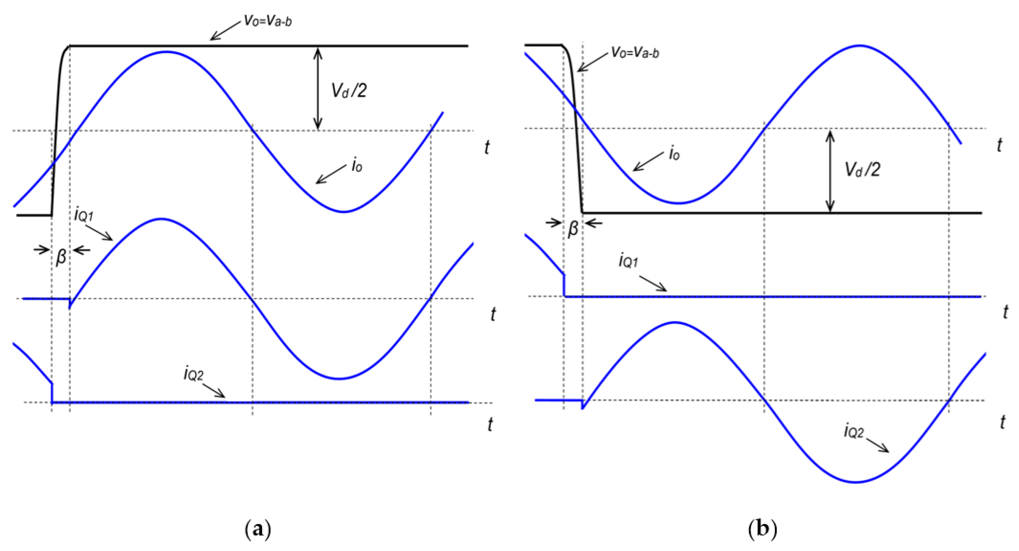
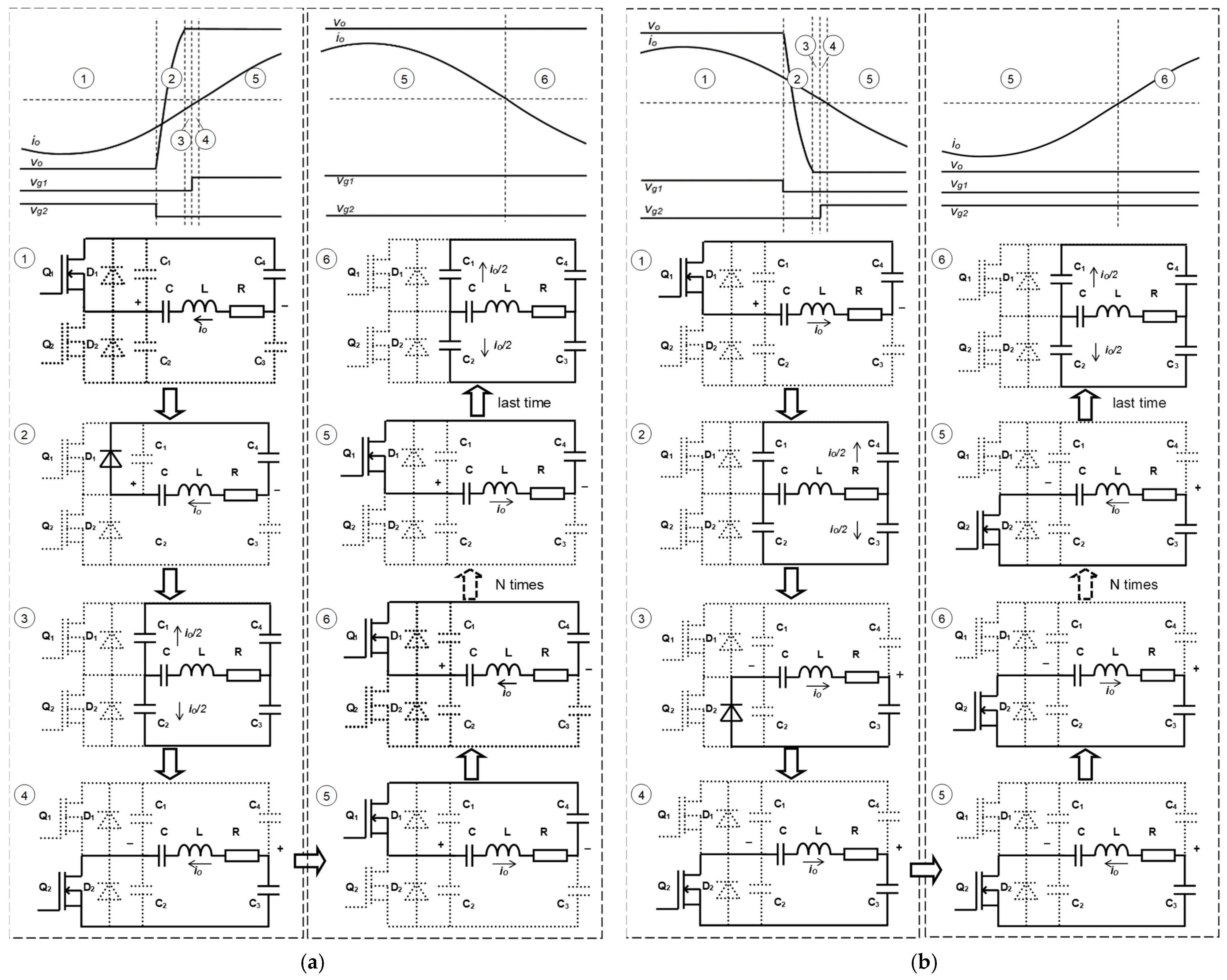
2.3. Control by Asymmetrical Pulse Width Modulation (APWM)
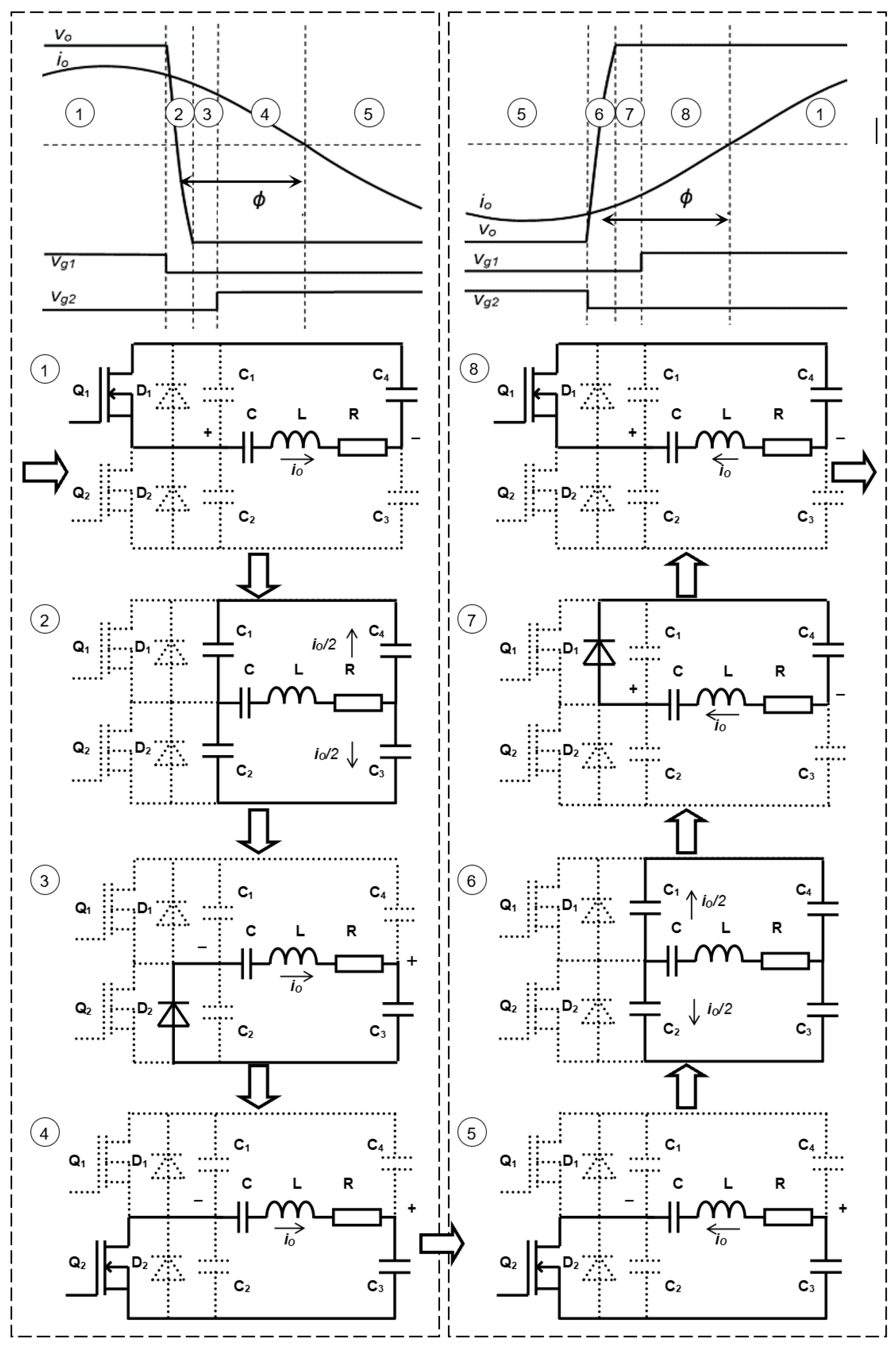
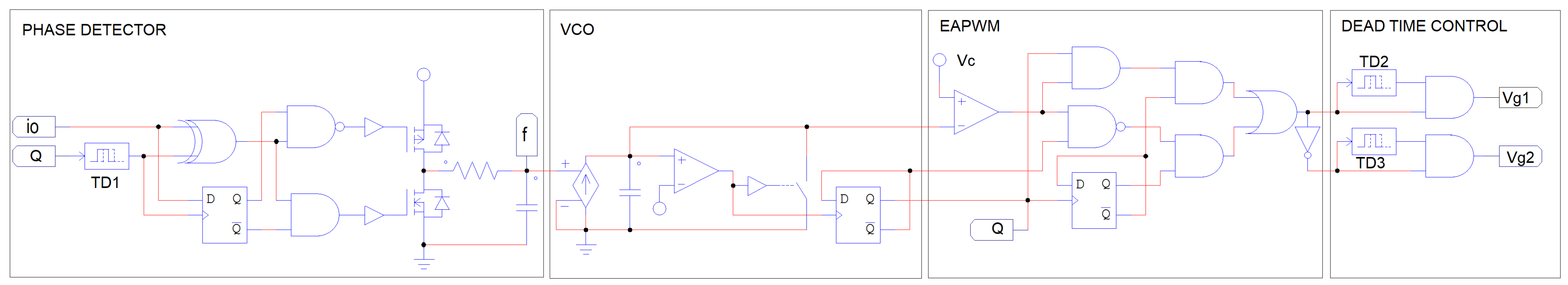
2.4. Control by Enhanced Asymmetrical Pulse Width Modulation (EAPWM)
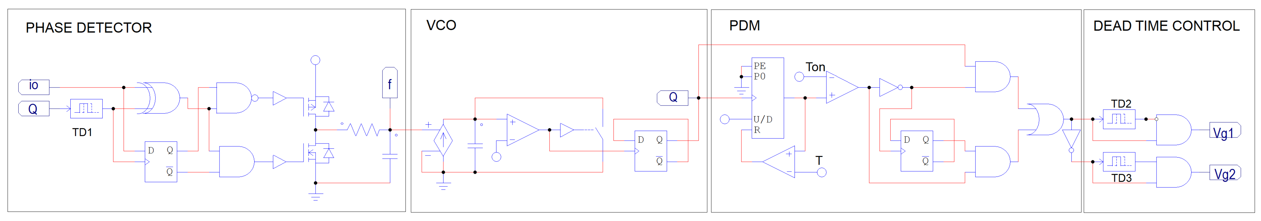
2.5. Control by Pulse Density Modulation (PDM)
2.6. Control by Enhanced Pulse Density Modulation (EPDM)
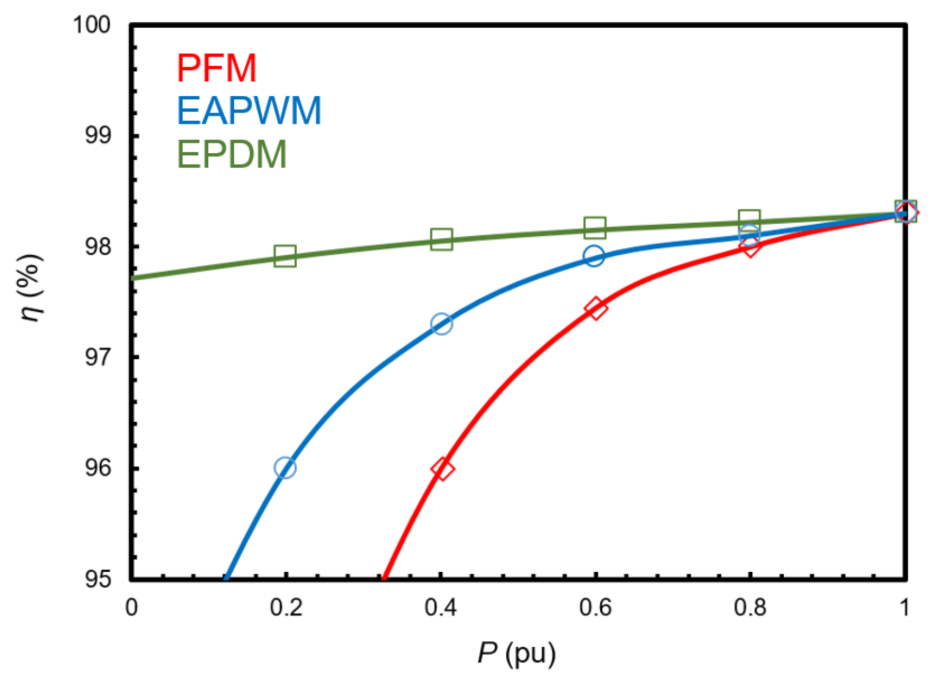
3. Results
3.1. Power Losses Analysis
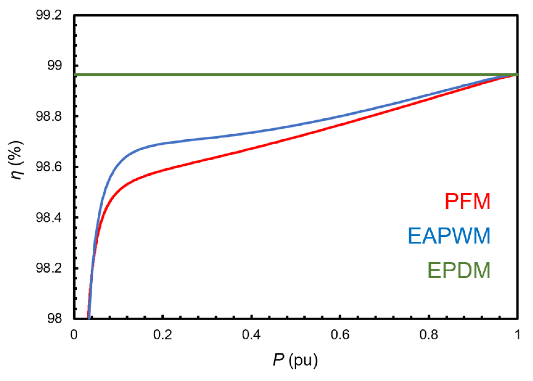
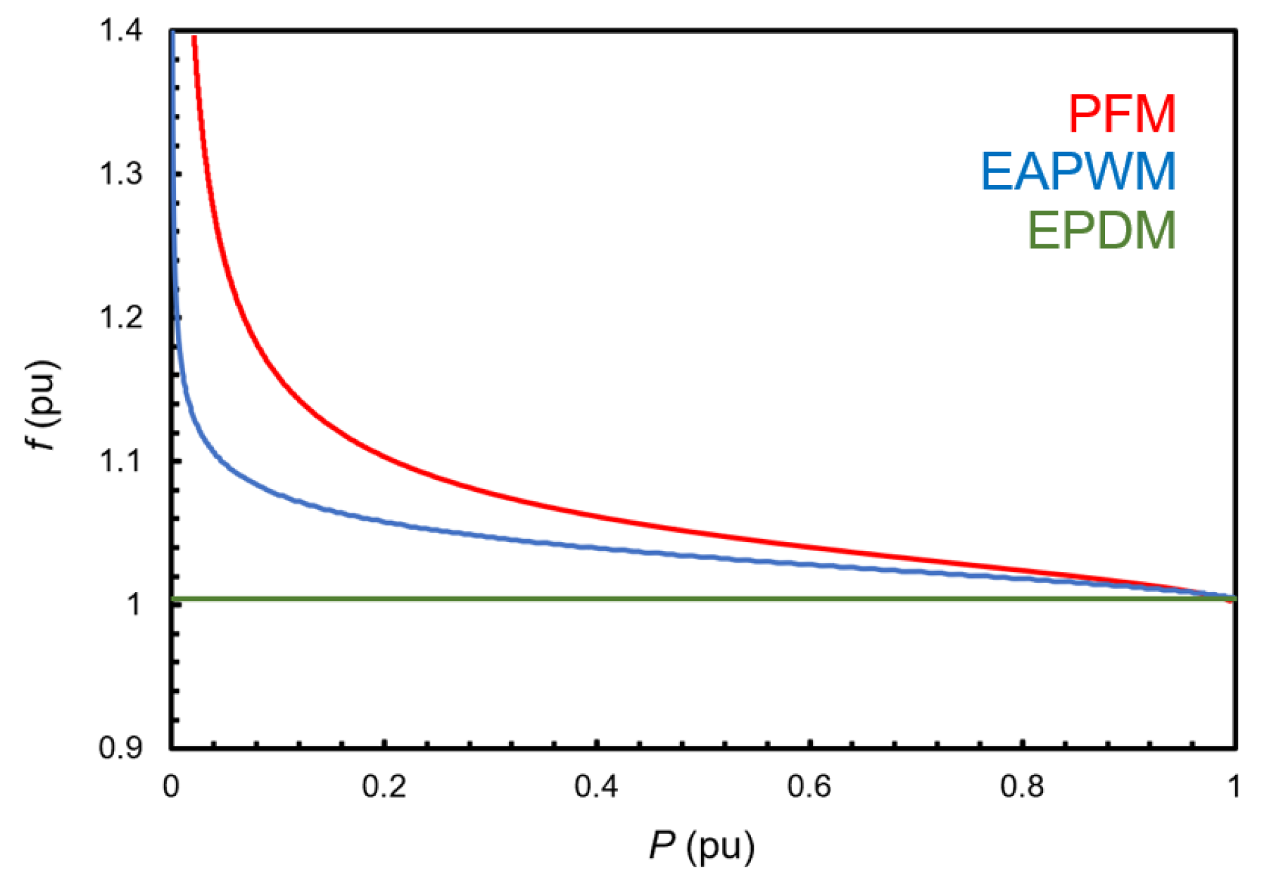
3.2. Comparative Study
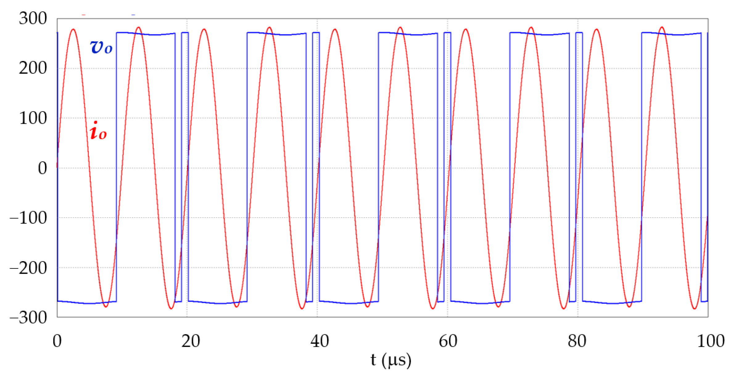
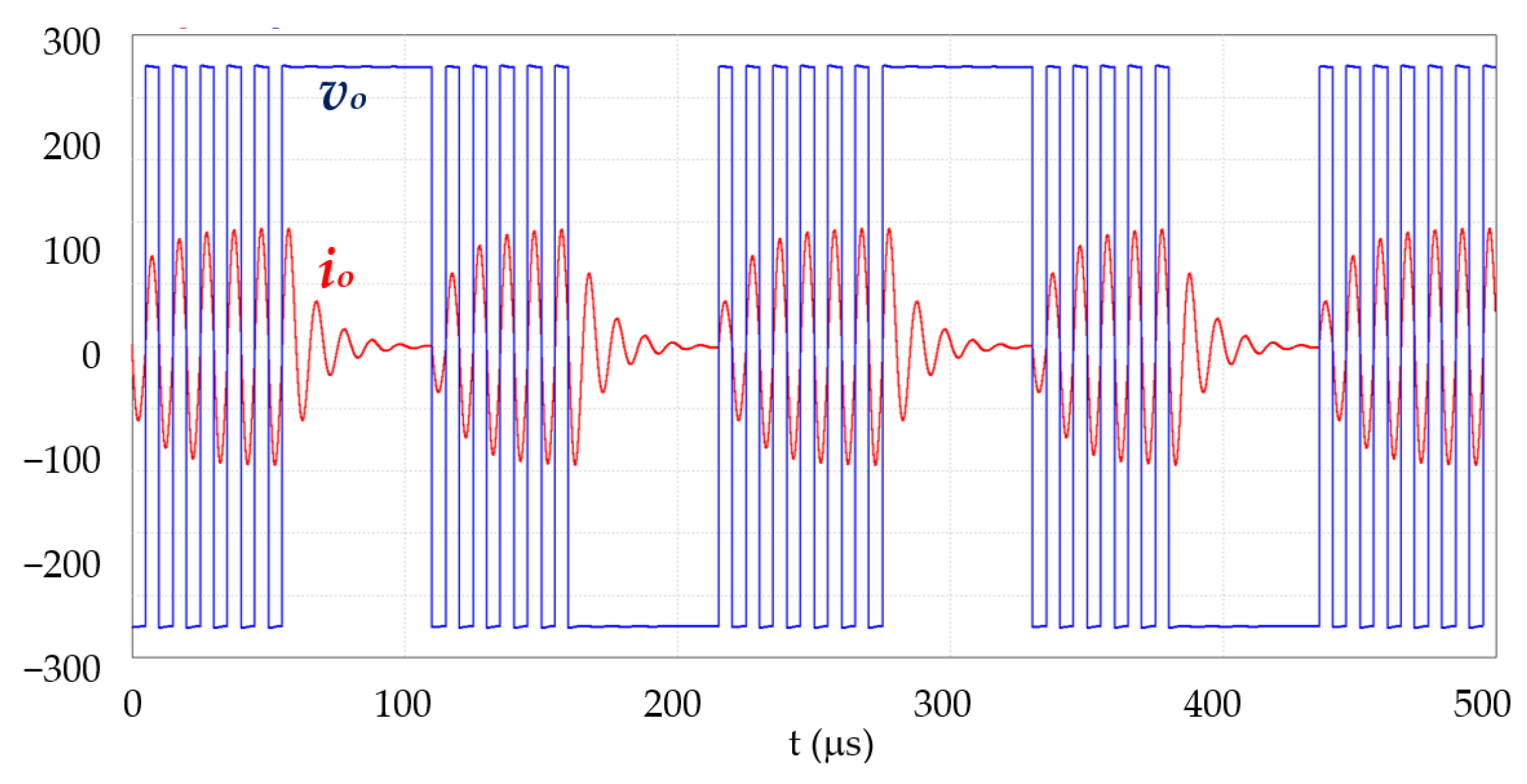
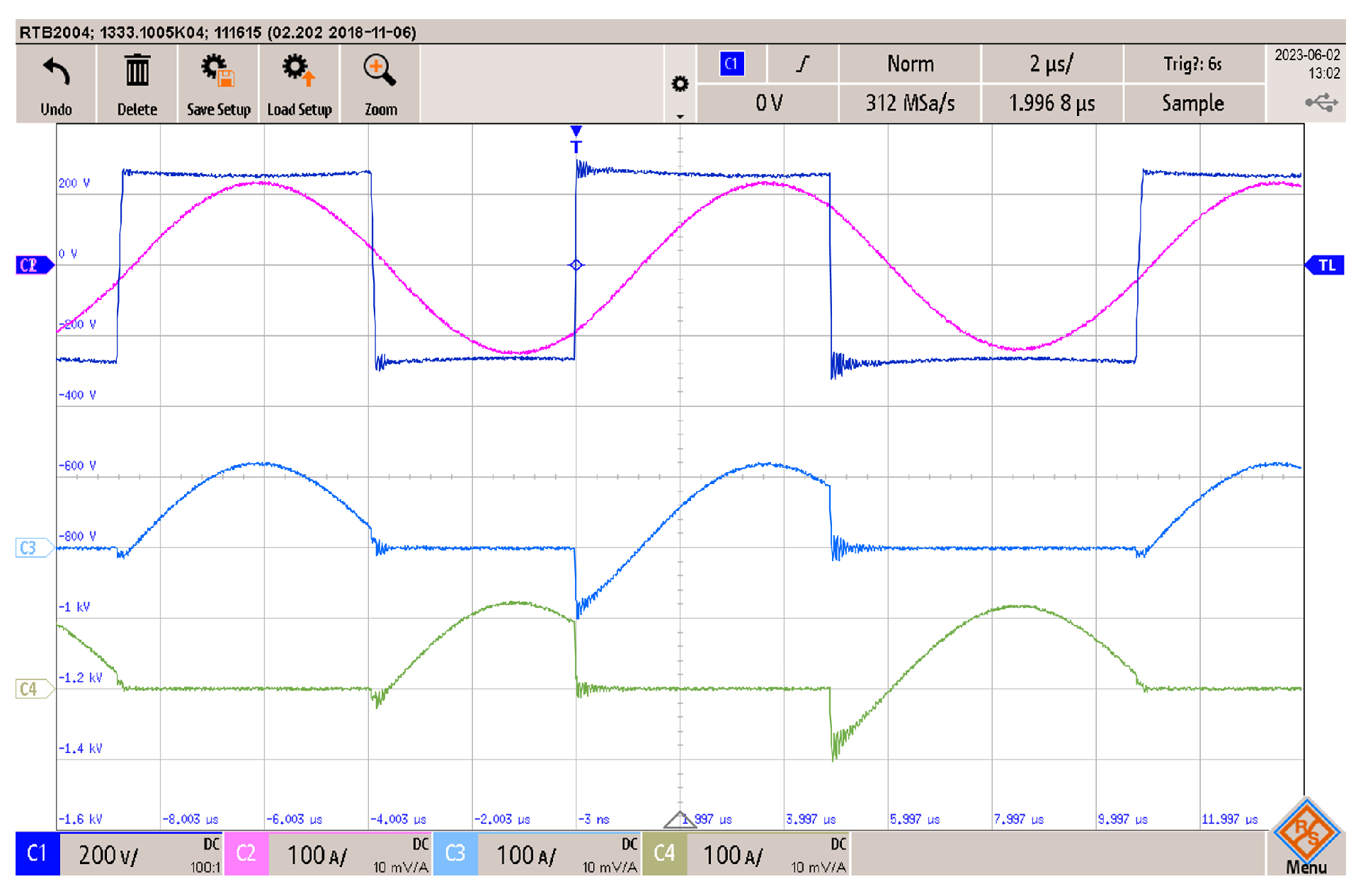
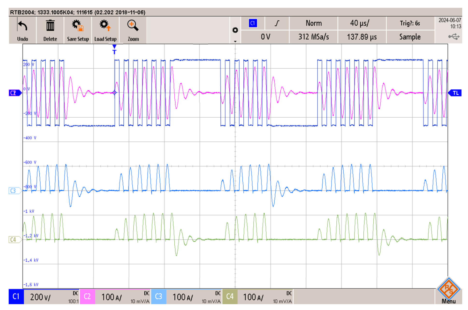
3.3. Experimental Results
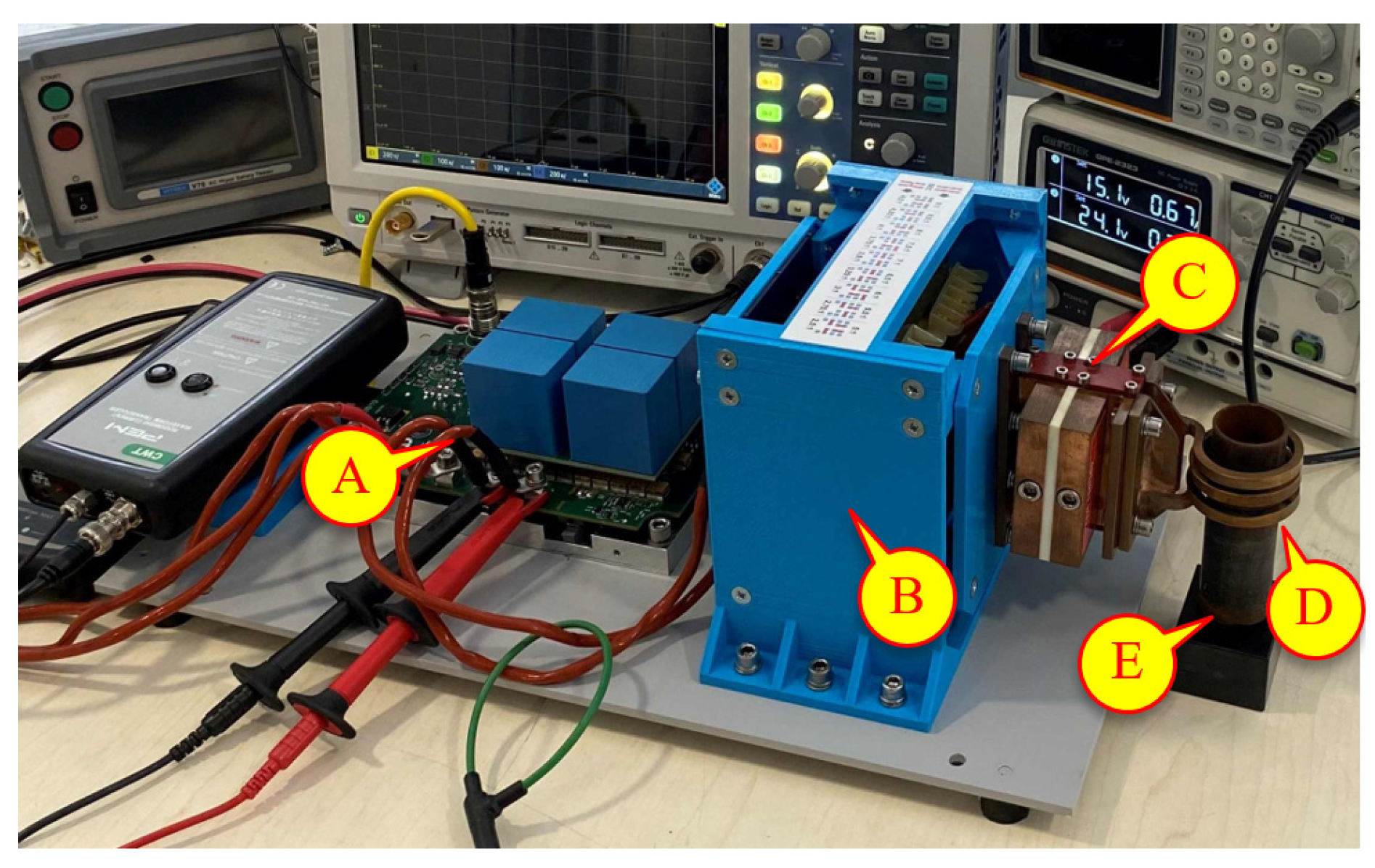
- A complete induction heating (A) converter that contained a HB-SRI inverter with two C3M0032120K SiC MOSFETs and four film capacitors of 33 μF, an input three phases rectifier, and an integrated digital electronic control on an FPGA-based system mounted on a water cooling heatsink.
- An output transformer (B) with n = 5:1
- Two high-power capacitors (C) of 2.5 μF connected in series, usable for induction heating.
- A solenoidal heating inductor (D) of 2 μH.
- A test load (E).
4. Conclusions
- The output power is regulated without varying the phase shift between the switches that compose the HB, and therefore, the efficiency remains high throughout the entire power range.
- The control circuit was designed to perform in ZVS condition.
- The variation in operating frequency is virtually negligible.
- The introduction of the alternative configuration of the active mode in the classic PDM modulation results in the DC component of the output voltage being zero and the losses in the two switches being balanced.
Author Contributions
Funding
Data Availability Statement
Conflicts of Interest
References
- Lucia, O.; Maussion, P.; Dede, E.J.; Burdio, J.M. Induction heating technology and its applications: Past developments, current technology, and future challenges. IEEE Trans. Ind. Electron. 2014, 61, 2509–2520. [Google Scholar] [CrossRef]
- Kawashima, R.; Mishima, T.; Ide, C. Three-Phase to Single-Phase Multiresonant Direct AC-AC Converter for Metal Hardening High-Frequency Induction Heating Applications. IEEE Trans. Power Electron. 2021, 36, 639–653. [Google Scholar] [CrossRef]
- Esteve, V.; Bellido, J.L.; Jordán, J. State of the Art and Future Trends in Monitoring for Industrial Induction Heating Applications. Electronics 2024, 13, 2591. [Google Scholar] [CrossRef]
- Erken, A.; Obdan, A.H. Induction Coil Design Considerations for High-Frequency Domestic Cooktops. Appl. Sci. 2024, 14, 7996. [Google Scholar] [CrossRef]
- Park, N.-J.; Lee, D.-Y.; Hyun, D.-S. A power-control scheme with constant switching frequency in class-d inverter for induction-heating jar application. IEEE Trans. Ind. Electron. 2007, 54, 1252–1260. [Google Scholar] [CrossRef]
- Faucher, S.; Forest, F.; Gaspard, J.-Y.; Huselstein, J.-J.; Joubert, C.; Montloup, D. Frequency-synchronized resonant converters for the supply of multiwinding coils in induction cooking appliances. IEEE Trans. Ind. Electron. 2007, 54, 441–452. [Google Scholar]
- Lucía, O.; Burdío, J.M.; Millán, I.; Acero, J.; Barragán, L.A. Efficiency oriented design of ZVS half-bridge series resonant inverter with variable frequency duty cycle control. IEEE Trans. Power Electron. 2010, 25, 1671–1674. [Google Scholar] [CrossRef]
- Dede, E.; Gonzalez, J.; Linares, J.; Jordan, J.; Ramirez, D.; Rueda, P. 25-kW/50-kHz generator for induction heating. IEEE Trans. Ind. Electron. 1991, 38, 203–209. [Google Scholar] [CrossRef]
- Shenkman, A.; Axelrod, B.; Chudnovsky, V. Assuring continuous input current using a smoothing reactor in a thyristor frequency converter for induction metal melting and heating applications. IEEE Trans. Ind. Electron. 2001, 48, 1290–1292. [Google Scholar] [CrossRef]
- Zhao, K.B.; Sen, P.C.; Premchandran, G. A thyristor inverter for medium-frequency induction heating. IEEE Trans. Ind. Electron. 1984, IE-31, 34–36. [Google Scholar] [CrossRef]
- Yilmaz, I.; Ermis, M.; Cadirci, I. Medium-frequency induction melting furnace as a load on the power system. IEEE Trans. Ind. Appl. 2012, 48, 1203–1214. [Google Scholar] [CrossRef]
- Pham, H.; Fujita, H.; Ozaki, K.; Uchida, N. Phase angle control of high-frequency resonant currents in a multiple inverter system for zone-control induction heating. IEEE Trans. Power Electron. 2011, 26, 3357–3366. [Google Scholar]
- Dawson, F.P.; Jain, P. A comparison of load commutated inverter systems for induction heating and melting applications. IEEE Trans. Power Electron. 1991, 6, 430–441. [Google Scholar] [CrossRef]
- Kazimierczuk, M.K.; Czarkowski, D. Resonant Power Converters; Wiley: New York, NY, USA, 1995. [Google Scholar]
- Lucia, O.; Burdio, J.M.; Millan, I.; Acero, J.; Puyal, D. Load-Adaptive Control Algorithm of Half-Bridge Series Resonant Inverter for Domestic Induction Heating. IEEE Trans. Ind. Electron. 2009, 56, 3106–3116. [Google Scholar] [CrossRef]
- Vishnuram, P.; Ramachandiran, G.; Sudhakar Babu, T.; Nastasi, B. Induction Heating in Domestic Cooking and Industrial Melting Applications: A Systematic Review on Modelling, Converter Topologies and Control Schemes. Energies 2021, 14, 6634. [Google Scholar] [CrossRef]
- Esteve, V.; Jordan, J.; Dede, E.J.; Sanchis-Kilders, E.; Martinez, P.J.; Maset, E.; Gilabert, D. Optimal LLC Inverter Design with SiC MOSFETs and Phase Shift Control for Induction Heating Applications. IEEE Trans. Ind. Electron. 2022, 69, 11100–11111. [Google Scholar] [CrossRef]
- Sarnago, H.; Lucía, Ó.; Mediano, A.; Burdío, J.M. Design and Implementation of a High-Efficiency Multiple-Output Resonant Converter for Induction Heating Applications Featuring Wide Bandgap Devices. IEEE Trans. Power Electron. 2014, 29, 2539–2549. [Google Scholar] [CrossRef]
- Aslan, S.; Ozturk, M.; Altintas, N. A Comparative Evaluation of Wide-Bandgap Semiconductors for High-Performance Domestic Induction Heating. Energies 2023, 16, 3987. [Google Scholar] [CrossRef]
- Cha, K.-H.; Ju, C.-T.; Kim, R.-Y. Analysis and Evaluation of WBG Power Device in High Frequency Induction Heating Application. Energies 2020, 13, 5351. [Google Scholar] [CrossRef]
- Esteve, V.; Sanchis-Kilders, E.; Jordan, J.; Dede, E.J.; Cases, C.; Maset, E.; Ejea, J.B.; Ferreres, A. Improving the Efficiency of IGBT Series-Resonant Inverters Using Pulse Density Modulation. IEEE Trans. Ind. Electron. 2011, 58, 979–987. [Google Scholar] [CrossRef]
- Ramalingam, S.R.; Boopathi, C.S.; Ramasamy, S.; Ahsan, M.; Haider, J.; Shahjalal, M. Single-Coil Multi-Tapped PDM-Based Induction Heating System for Domestic Applications. Electronics 2023, 12, 404. [Google Scholar] [CrossRef]
- Sarnago, H.; Lucía, Ó.; Mediano, A.; Burdío, J.M. Analytical Model of the Half-Bridge Series Resonant Inverter for Improved Power Conversion Efficiency and Performance. IEEE Trans. Power Electron. 2015, 30, 4128–4143. [Google Scholar] [CrossRef]
- Mollov, S.; Theodoridis, M.; Forsyth, A. High frequency voltage-fed inverter with phase-shift control for induction heating. Proc. Inst. Electr. Eng. Electr. Power Appl. 2004, 151, 12–18. [Google Scholar] [CrossRef]
- Esteve, V.; Jordán, J.; Dede, E.J.; Bellido, J.L. Enhanced asymmetrical modulation for half-bridge series resonant inverters in induction heating applications. IET Power Electron. 2023, 16, 2482–2491. [Google Scholar] [CrossRef]
- Esteve, V.; Jordan, J.; Sanchis-Kilders, E.; Dede, E.J.; Maset, E.; Ejea, J.B.; Ferreres, A. Enhanced Pulse-Density-Modulated Power Control for High-Frequency Induction Heating Inverters. IEEE Trans. Ind. Electron. 2015, 62, 6905–6914. [Google Scholar] [CrossRef]
- Acero, J.; Lucia, O.; Millan, I.; Barragan, L.A.; Burdio, J.M.; Alonso, R. Identification of the material properties used in domestic induction heating appliances for system-level simulation and design purposes. In Proceedings of the 2010 IEEE Applied Power Electronics Conference and Exposition, APEC’10, Palm Springs, CA, USA, 21–25 February 2010; pp. 439–443. [Google Scholar]
- Esteve, V.; Dede, E.J.; Jordan, J.; Cases, C.; Herrero, R.; Magraner, J.M.; Maset, E. Stabilization of the DC-link for inverters with PDM power control. In Proceedings of the 2009 13th European Conference on Power Electronics and Applications, Barcelona, Spain, 8–10 September 2009; pp. 1–9. [Google Scholar]
- Rui, W.; Qiuye, S.; Dazhong, M.; Dehao, Q.; Yonghao, G.; Peng, W. Line Inductance Stability Operation Domain Assessment for Weak Grids with Multiple Constant Power Loads. IEEE Trans. Energy Convers. 2021, 36, 1045–1055. [Google Scholar] [CrossRef]
- Fujita, H.; Akagi, H. Pulse-density-modulated power control of a 4 kW, 450 kHz voltage-source inverter for induction melting applications. IEEE Trans. Ind. Appl. 1996, 32, 279–286. [Google Scholar] [CrossRef]
- Lo, J.K.; Lin, C.-Y.; Hsieh, M.-T.; Lin, C.-Y. Phase-Shifted Full-Bridge Series-Resonant DC-DC Converters for Wide Load Variations. IEEE Trans. Ind. Electron. 2011, 58, 2572–2575. [Google Scholar] [CrossRef]
- Lucia, O.; Burdio, J.M.; Barragan, L.A.; Carretero, C.; Acero, J. Series Resonant Multiinverter with Discontinuous-Mode Control for Improved Light-Load Operation. IEEE Trans. Ind. Electron. 2011, 58, 5163–5171. [Google Scholar] [CrossRef]
- Imbertson, P.; Mohan, N. Asymmetrical duty cycle permits zero switching loss in PWM circuits with no conduction loss penalty. IEEE Trans. Ind. Appl. 1993, 29, 121–125. [Google Scholar] [CrossRef]
- Esteve, V.; Jordán, J.; Dede, E.J.; Martinez, P.J.; Ferrara, K.J.; Bellido, J.L. Comparative analysis and improved design of LLC inverters for induction heating. IET Power Electron. 2023, 16, 1754–1764. [Google Scholar] [CrossRef]


| Component | Symbol | Value | Unit |
|---|---|---|---|
| Nominal Output Power | Po | 18 | kW |
| Nominal Frequency | fo | 100 | kHz |
| DC Input Voltage | Vd | 540 | V |
| Resonant Inductor | L | 2 | μH |
| Output Quality Factor | Q | 10 | |
| Transformer Ratio | n | 5 | |
| Resonant Capacitor | C | 1.27 | μF |
| Equivalent Series Resistor | R | 126 | mΩ |
| Magnitude | Symbol | Value | Unit |
|---|---|---|---|
| Second order coefficient | a | 0.0546 | µJA−1/2 |
| First order coefficient | b | −1.7479 | µJA−1 |
| Constant term | c | 37.8 | µJ |
| Magnitude | Symbol | Value | Unit |
|---|---|---|---|
| Maximum power loss per transistor | Pmax | 94.6 | W |
| Thermal resistance junction to case | RthJC | 0.44 | K/W |
| Thermal resistance case to heatsink | RthCH | 0.2 | K/W |
| Thermal resistance heatsink to ambient | RthHA | 0.3 | K/W |
| Ambient temperature | TA | 40 | °C |
| Maximum junction temperature | TJmax | 124.2 | °C |
Disclaimer/Publisher’s Note: The statements, opinions and data contained in all publications are solely those of the individual author(s) and contributor(s) and not of MDPI and/or the editor(s). MDPI and/or the editor(s) disclaim responsibility for any injury to people or property resulting from any ideas, methods, instructions or products referred to in the content. |
© 2025 by the authors. Licensee MDPI, Basel, Switzerland. This article is an open access article distributed under the terms and conditions of the Creative Commons Attribution (CC BY) license (https://creativecommons.org/licenses/by/4.0/).
Share and Cite
Esteve, V.; Jordán, J.; Bellido, J.L. Optimizing the Efficiency of Series Resonant Half-Bridge Inverters for Induction Heating Applications. Electronics 2025, 14, 1200. https://doi.org/10.3390/electronics14061200
Esteve V, Jordán J, Bellido JL. Optimizing the Efficiency of Series Resonant Half-Bridge Inverters for Induction Heating Applications. Electronics. 2025; 14(6):1200. https://doi.org/10.3390/electronics14061200
Chicago/Turabian StyleEsteve, Vicente, José Jordán, and Juan L. Bellido. 2025. "Optimizing the Efficiency of Series Resonant Half-Bridge Inverters for Induction Heating Applications" Electronics 14, no. 6: 1200. https://doi.org/10.3390/electronics14061200
APA StyleEsteve, V., Jordán, J., & Bellido, J. L. (2025). Optimizing the Efficiency of Series Resonant Half-Bridge Inverters for Induction Heating Applications. Electronics, 14(6), 1200. https://doi.org/10.3390/electronics14061200