Article

LTSPICE Memristor Neuron with a Modified Transfer Function Based on Memristor Model with Parasitic Parameters †

Faculty of Automatics, Department of Fundamentals of Electrical Engineering, Technical University of Sofia, 8 Kliment Ohridski Blvd., 1000 Sofia, Bulgaria
*
Author to whom correspondence should be addressed.
This paper is an extended version of a paper presented in MOCAST 2024 Conference, Sofia, Bulgaria, 26–28 June 2024.
Electronics 2025, 14(23), 4645; https://doi.org/10.3390/electronics14234645
Submission received: 5 November 2025 / Revised: 18 November 2025 / Accepted: 20 November 2025 / Published: 26 November 2025
(This article belongs to the Special Issue Modern Circuits and Systems Technologies (MOCAST 2024))

Abstract

Memristors, as novel one-port electronic elements, have very good memory and commutating properties, insignificant power consumption, and a good compatibility to present CMOS integrated chips. They are applicable in neural networks, memory arrays, and various electronic devices. This paper proposes a simple LTSPICE model of an adapted activation function and a neuron built on memristors. In the neuron, synaptic bonds are implemented by single memristors, allowing a decreased circuit complexity. The summing and scaling schemes are based on op-amps and memristors. The applied modified tangent-sigmoidal activation function is implemented with MOS transistors and memristors. Analyses and simulations are conducted using a simple and high-rate operating memristor model with parasitic parameters—resistance, inductance, capacitance, and small-signal DC components. Their influence on the normal operation of the memristors in the neuron is analyzed, paying attention to their usage and adjustment. The proposed memristor-based artificial neuron is analyzed in MATLAB–Simulink and LTSPICE simulators. A comparison between the derived results confirms the correct operation of the proposed memristor neuron. The generation and analyses of the suggested memristor-based neuron is a significant and promising step for the design and engineering of high-complexity neural networks and their realization in ultra-high-density integrated neural circuits and chips.

1. Introduction

The electro-chemical communications in biological neural cells, analyzed in human brain and other organisms are the main motivating reasons for the generation of artificial and spiking neural networks [1]. Artificial neural networks and schemes are energy-effective and high-speed ones. They could perform complex computing tasks and have promising applications in low-power electronic circuits for artificial intelligence (AI) [2]. Neural networks based on MOS transistors and optical devices were regularly used in the past. Nowadays, some of the newest achievements in this area are the neural networks, based on memristors, which are generally used for realization of synaptic weights [3,4]. Memristors, also known as “memory resistors”, are two-terminal, passive electronic components that have the ability to partially hold their state and resistance in relation to the passed electrical charges [5]. Their state and conductance could be changed by applied voltage or current impulses. Many times, memristors are employed as tunable resistors [6,7]. Frequently, doped metal oxides are utilized for memristor realizations. Generally, memristors have very low power utilization, good switching and memory properties, high operating rate, nano-scale dimensions, and very good compatibility with the present integrated CMOS circuits [8]. Usually, memristors are fabricated as crossbars and arrays, included in integrated circuits. They are easily applicable in neural networks, memory arrays, and various other electronic circuits and devices. In artificial neural networks, they are commonly used for synaptic realization [9,10]. Various types of memristor-based synapses and neurons are reported in the scientific literature [7,8]. A drawback in some synapses, founded on single memristors and MOS transistors, is the realization of only positive synaptic weights. Other complex neural schemes contain two and more memristor elements per synapse. Bridge memristor synapses guarantee negative, zero, and positive synaptic weights [7]. Their key disadvantage is the bigger number of memristors per synaptic connection. Commonly, three or more memristor elements are employed, and two or more op-amps are used. An opportunity for realization of each synapse by only one memristive element is available, and this significantly decreases the neural circuits’ complexity [11]. Sometimes, the variations in parameters of memristors could affect the synaptic weights, and thus the robustness, accuracy, convergence, efficiency, and operating speed of artificial neurons could be changed. For efficient analysis of memristor-based neurons in complex neural networks, high-speed and simple SPICE memristor models are needed for reducing the simulation time [11,12,13].
In this work, an improved and simplified LTSPICE memristor model with parasitic parameters [14,15] is proposed. The unavoidable parasitic capacitance, inductance, and resistance are addressed. Additional small-signal DC voltage and current sources are used for expressing the shifting of the cross-section of the i-v curve according to the origin of the coordinate system at high-frequency signals [14,16]. Activation voltage threshold [16] is incorporated in the suggested memristor models. Along with the other SPICE family products, like Or CAD PSPICE, HSPICE, Micro-Cap, and others, LTSPICE is a preferable software simulator [11,12,17]. It has a user-friendly interface and free license. It has good convergence properties and no restrictions on the number of electronic elements and their connections [11,12]. The LTSPICE software simulator, together with MATLAB and Simulink, are used for the conducted analyses in this work.
After a detailed reference check, it was established that a few publications provide complete structures of memristor synapses, neurons, and activation functions, modeled in electronic simulators, and corresponding results with comparisons. This was the general motivation for the present research. The purpose of this paper is to propose a simple memristor neuron in LTSPICE, having negative and positive synaptic weights, using the least number of electronic elements. A total implementation of a memristor-based neuron in LTSPICE is presented. A modified activation function with MOS transistors and memristors is suggested. A modified and simple memristor model with parasitic parameters is presented. The influence of related parasitic parameters on the normal operation of the memristor-based neuron is analyzed in LTSPICE.
The rest of the paper is presented as follows. Section 2 briefly presents memristor structure, operation, and modeling. Experimental investigation, adjustment in MATLAB–Simulink, generation, and analysis of the corresponding LTSPICE model are described in Section 3. The proposed LTSPICE memristor-based neuron and transfer functions are discussed in Section 4. The results derived are compared and commented on in Section 5. A discussion is provided in Section 6. The conclusion of the paper is presented in Section 7.

2. Memristors, Modeling, and LTSPICE Implementation

Here, a brief explanation of memristors’ fundamentals is first offered for a better understanding of their structure, operation, modeling, and investigations [13,16].

2.1. Structure of Memristor Elements and Their Operation

There are many kinds of memristors—metal-oxide-based ones, metal-chalcogenide, polymeric, ferroelectric, and others [18,19,20]. Metal-oxide [20] and metal-chalcogenide memristors [18,19] are in the focus of the present research, owing to their stable characteristics, good memory, and switching properties, which are based on passing of electric charges under applied voltage or current electric pulses. For better understanding of their operation, a simple schematic of a metal-oxide memristor is presented in Figure 1a. It contains two metallic electrodes, denoted as anode (a) and cathode (c). The active layer is based on a metallic oxide, partially doped by oxygen vacancies [20]. The size of the doped layer is denoted as w, while the complete memristor structure has a length of D. The state variable x is represented as a ratio between the sizes of the doped layer and those of the whole memristor element [5]. It is restricted in the scope between zero and one, owing to the limited sizes of the memristor element.
The main parasitic parameters are as follows: resistance, inductance, and capacitance [14,15]. The parasitic resistance is denoted by Rpar, and it represents the unavoidable resistance of the metallic electrodes. The parasitic inductance is represented as Lpar. It is related to generation of magnetic fields around the current paths in the memristor [14]. Parasitic capacitance Cpar is related to the equivalent elementary capacitor, created between the metallic electrodes of the memristor [14]. Different models are available, related to the equivalent schematics of the metal-oxide memristor [14]. In [15], parasitic capacitance Cpar is directly connected to the memristor nanostructure. In the present research, another model is proposed. It is related to attachment of the parasitic capacitance to the input terminals of the memristor. In this way, the other possible and additional capacitances are included in the considered capacitance [14]. The additional small-signal DC voltage and current sources Jpar and Lpar are included for representation of the shifting of the i-v pinched hysteresis loop for middle and high-frequency signals [14,15]. Figure 1b represents the corresponding equivalent scheme of the metal-oxide memristor. The memristor nanostructure is presented, according to the scheme of Figure 1a, as a series connection of two state-dependent and nonlinear resistors [5,16].
The current–voltage relations of the discussed parasitic elements are presented with Formula (1) [15]. They will be utilized in the next paragraphs for memristor modeling.
v R p a r = R p a r i L p a r ;   v L p a r = L p a r d i L p a r d t ;   i C p a r = C p a r d v t o t a l d t

2.2. Memristor Modeling

In the theory of memristor modeling, at least two equations are needed for defining a memristor model [16]. The first one represents the current-voltage relation. It includes the memristance M(x) or the memductance G(x), which are state-dependent quantities [16]. The following equation relates the memristor voltage (or current) to the time derivative of memristor state variable x [5]. A big assembly of regularly employed models of voltage-controlled memristors, like these of Strukov–Williams [5], Joglekar [21], Biolek [10], and Prodromakis [22] is described by the next system (2).
v m e m = M x i m e m = R O N x + R O F F 1 x i m e m d x d t = x ˙ = k · i m e m v m e m · f x ;   x t = 0 = x 0
The measures RON and ROFF are the ON-state and OFF-state memristances, k is a physical parameter of the memristor element, imem and vmem are the memristor voltage and current, x0 is the initial value of the state variable at time t = 0, and f(x) represents a window function [11]. It is applied for restricting the memristor state variable in the range between zero and unity.
In the next paragraph, the proposed memristor models B6m and B6par are discussed.

2.3. The Proposed Memristor Model (B6m)

The proposed modified memristor model without parasitic parameters is denoted as B6m and is presented in Formula (3). The first equation relates the memristor current imem to its voltage vmem. The quantities RON and ROFF are the limiting values of its memristance. The initial value of the state variable is x0. The third expression represents the state differential equation. It is based on the standard Lehtonen–Laiho model, according to the time derivative of the state variable [20]. The quantity η is a polarity coefficient. For a forward-biased memristor, it has a value of 1, and it is −1 if the memristor is connected in a reverse direction. The applied window function is the standard and simple parabolic Strukov–Williams window. A voltage activation threshold vthr is applied in the model. The final expression presents a smooth and differential step-like function; it is very similar to the classical Heaviside step function [9]. The coefficient m has negative values and determines the steepness of this function. If the memristor voltage vmem is lower than the activation threshold vthr, then the element behaves as a simple and linear resistor. In this mode, the state variable has a constant value [16]. When the memristor voltage is equal or higher than the activation threshold, then the state variable changes proportionally to the time integral of the applied memristor voltage.
v m e m = R O N x + R O F F 1 x · i m e m x t = 0 = x 0 d x d t = x ˙ = η · k · v m e m 3 · x x 2 · f t h r v t h r , v m e m f t h r v t h r , v m e m = 1 1 + exp m · v m e m v t h r
The first equation in (3) represents symmetrical current–voltage relations [5]. It is based on Strukov–Williams memristor model [5].
The modified memristor model with parasitic parameters is denoted as B6par and is presented with system (4). It is founded on (2) and (3) and on the memristor model presented in Figure 1b.
v m e m = i m e m · R O N x + R O F F 1 x ,   x t = 0 = x 0 d x d t = x ˙ = η k v m e m 3 x x 2 1 1 + exp m · v m e m v t h r i C p a r = C p a r d d t v t o t a l ;   i L p a r = i R p a r = i m e m J p a r i t o t a l = i L p a r + i C p a r v t o t a l + i L p a r R p a r + v m e m E p a r + L p a r d d t i L p a r = 0
The current through the parasitic capacitance iCpar is expressed, applying the definition for a current through a capacitor [16]. The current through the parasitic inductor is expressed as a difference between the current through the memristor and the current of the DC current source Jpar, according to the topology of the presented schematic. The total input current itotal is expressed by an algebraic summation of the currents through the parasitic inductor and capacitor, according to the KCL. The final equation is written for the loop, including the input signal vtotal, the parasitic resistor Rpar, and inductor Lpar, the additional DC voltage source Epar, and the memristor, according to the KVL.
The inclusion of the discussed parasitic parameters additionally increases the memristor model complexity. In many cases and at different frequencies, only one or two of the discussed parasitic parameters are really needed. For keeping the memristor model with a comparatively low complexity, only the important parasitic parameters, which affect the normal operation of the memristors in a significant extent, should be included. The parasitic parameters with a low influence could be ignored.

3. Experimental Investigation, Adjustment in MATLAB–Simulink, and Generation and Analysis of the Corresponding LTSPICE Memristor Model

3.1. Experimental Measurements

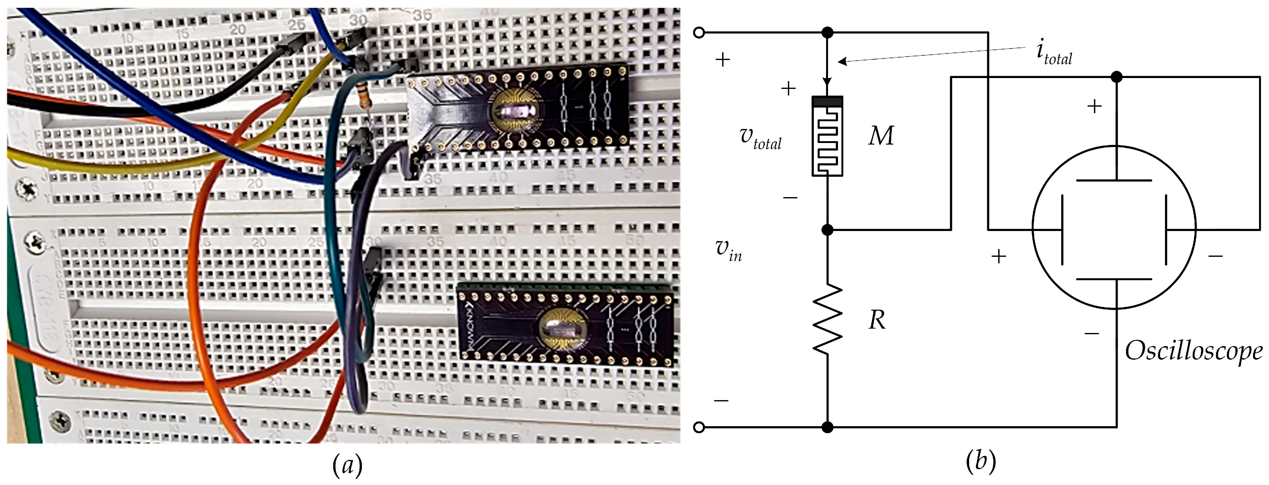
Here the utilized experimental setup equipment for the measurement of the current–voltage relations of Knowm memristors are discussed [18,19]. Usually, Knowm memristors are related to asymmetrical i-v relations. The memristors under analysis are included in integrated circuits, presented in Figure 2a. An electronic breadboard and a digital oscilloscope are also used. A computer with intel i5, 2-core 2.4 GHz processor, 512 SSD, 8 GB RAM, and MS Windows 10 Pro is used for computer simulations. As specialized software, MATLAB–Simulink [23,24] version R2016a and LTSPICE XVII [12,13] are utilized for the present analyses. One of the Knowm memristors is randomly selected for the investigations. A limiting resistor with a value of 10 kΩ is connected in a series to the memristor element. It is applied for restricting the memristor current and for protection of the memristor element from high-valued currents [25].
A principal schematic related to Figure 2a is presented in Figure 2b. The memristor voltage denoted as vtotal is applied to the horizontal channel of the oscilloscope. Its vertical channel is connected to the limiting resistor R, whose voltage is proportional to the memristor current. This schematic is used for visualization and recording of the current–voltage relations of the Knowm memristor at applied different sine-wave and pulse signals at different amplitudes and frequencies. The i-v characteristics are first visualized and then recorded as .csv files, which are converted to .xls format and applied for parameter estimation in Simulink, described in Section 3.2 [23,24].

3.2. Adjustment of the Proposed Memristor Model in MATLAB–Simulink, According to the Experimental Data of Knowm Memristors [19]

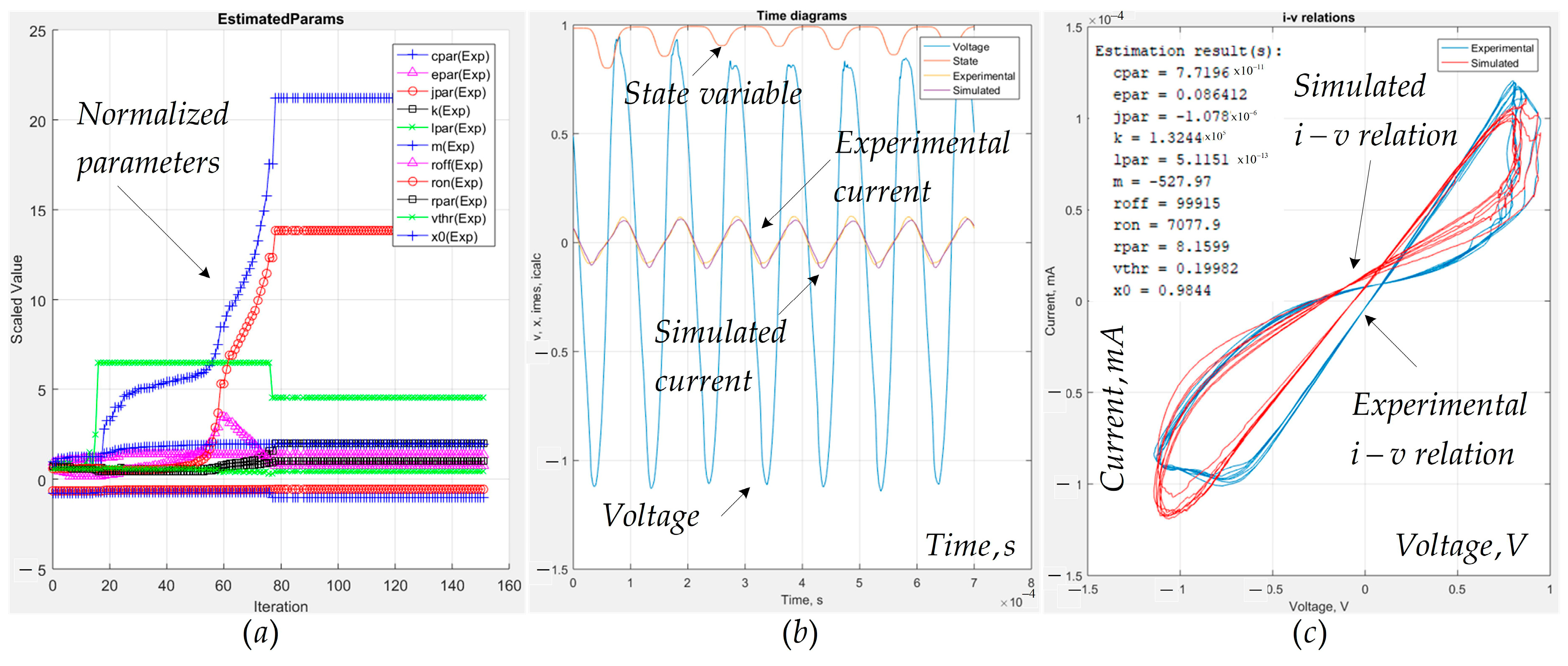
The modified memristor model with parasitic parameters, denoted as B6par and presented by (4), is tuned in the MATLAB–Simulink environment, utilizing experimentally recorded current–voltage relationships of self-directed channel Knowm memristors [19]. The initial values of the model’s parameters are randomly selected. Two .xls files are used. The first one contains two columns. The first column represents the time variable, sampled with a time step of 100 ps, corresponding to a sample frequency of 10 GHz. The time variable is denoted as tout. The second column corresponds to the sampled voltage signal, applied to the Simulink memristor model under analysis. This signal is denoted as vtotal. The second .xls file has a similar structure, but its second column represents the experimental current of the memristor element. It is denoted as imes. A Simulink model is generated according to system (4). The described above .xls files are used as a voltage source and as a reference memristor current, respectively. As an output signal, the Simulink model generates the simulated memristor current, denoted as itotal. The parameter estimation procedure is based on gradient descent algorithm. As a cost function, the squared difference between the simulated and the experimental memristor currents is used. The standard number of iterations is about 100. The end of the estimation procedure is reached when the number of iterations is finished or when the cost function is equal or lower than a previously determined value [23,24]. After finishing the parameter estimation procedure, a low relative error of about several percent between the experimental and the simulated i-v relations is obtained. Minimization of the root mean square error (RMSE) between the experimental and simulated characteristics is reached.
The trajectories of the model’s parameters during estimation process are presented in Figure 3a. Their normalized values are presented. The time diagrams of experimental and simulated memristor currents, together with the state variable and the applied voltage, are given in Figure 3b for their visual comparison. Additional comparison is presented using the simulated and experimental i-v relations, shown in Figure 3c. It is visible that a good proximity between these characteristics is established.
The derived optimal values of memristor model parameters after finishing the optimization procedure are Rpar = 8.16 Ω, Lpar = 0.51 pH, Jpar = −1.08 uA, Epar = 0.086 V, Cpar = 77.2 pF, k = 132440, x0 = 0.9844, RON = 7077.9 Ω, ROFF = 99.915 kΩ, m = −527.98, and vthr = 0.1998 V.

3.3. Generation and Analysis of the Corresponding LTSPICE Memristor Models

Using Equation (3) and the memristor model parameters, discussed in the previous Section 3.2, LTSPICE memristor library model without parasitic parameters is generated. It is denoted as B6m. The corresponding LTSPICE code is presented below for additional discussion.
  • . subckt B6m a c Y
  • .params m0=10e3 ron=7077.9 roff=99.915e3 k=132.44e3 vthr=0.1998
  • C1 Y 0 {1}
  • . IC V(Y)={(roff-m0)/(roff-ron)}
  • R1 Y 0 10G
  • G2 0 Y value={(k*pow(V(a,c),3)*(V(Y)*(1-V(Y))))*(1/(1+exp(−527.987*(abs(V(a,c))-vthr))))}
  • G1 a c value={V(a,c)*((1/(ron*(V(Y))+roff*(1-V(Y)))))}
  • .ends B6m
The code starts with the LTSPICE command “.subckt”, defining the new circuit element. It is followed by its abbreviation “B6m” and its main terminals—anode “a” and cathode “c”. The terminal Y is an optional one. It could be placed for the measuring of the memristor state variable x. The main model parameters are visualized in the next row of the code. This is followed by the integrating capacitor C1, connected between the ground and the terminal Y. Its voltage is proportional to the state variable x. The next row determines the initial value of the state variable x0, using the initial memristance m0, and the ON-state and OFF-state resistances. The fifth row introduces an additional resistor—R1, connected in parallel to the integrating capacitor C1. The current of the controlled source G2, presented in the next row, is proportional to the time derivative of memristor state variable x. It corresponds to system (3). The voltage across the memristor is denoted as V(a,c). The applied parabolic window function is (V(Y)*(1-V(Y)))), where V(Y) is related to the state variable x. The dependent current source G1 represents the memristor current. The presented LTSPICE code finishes with the command “.ends”. The presented code could be easily adapted for use in another SPICE family software products, using Verilog-A [26]. It could be an alternative for analysis of composite- and halide-perovskite-based memristors, with applications in logic gates and functions. Noises in electronic schemes affect to some extent the normal operation of memristors and memristor-based circuits [27,28]. Usually, they are related to fluctuations of some properties and parameters of the materials. The noises slightly affect memristor accuracy, read/write operations, and memory and switching properties.
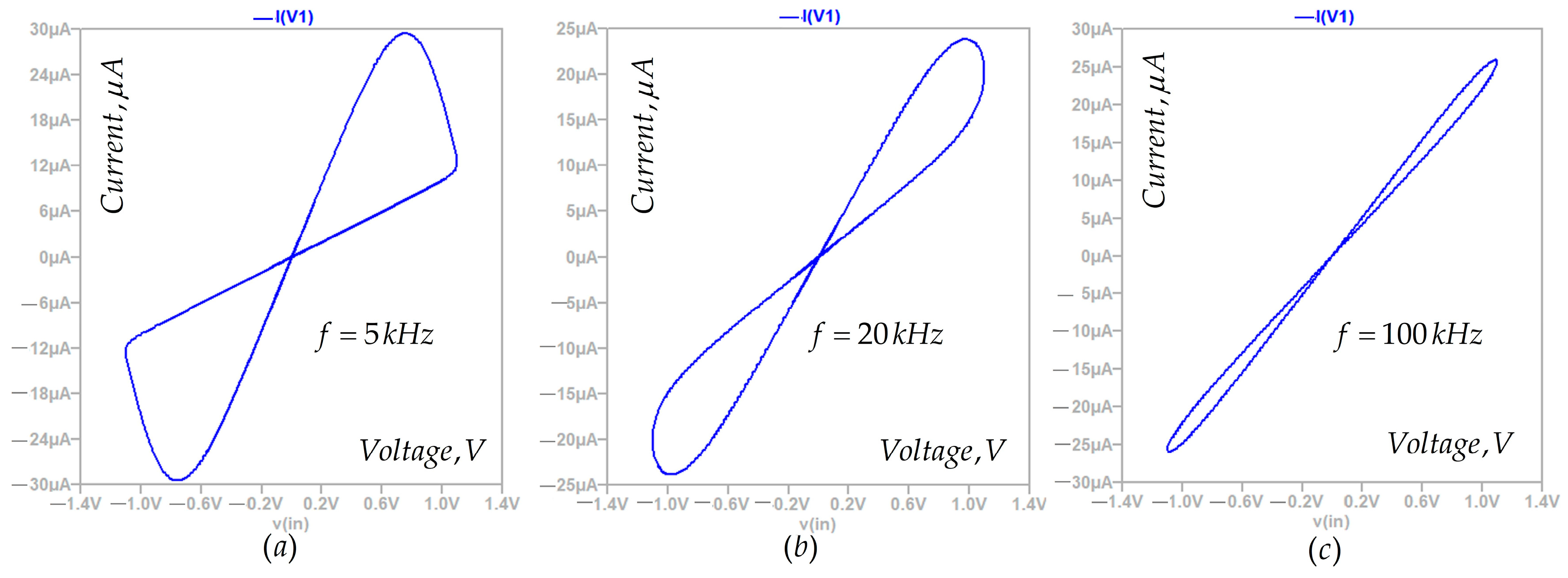
For the conducted analyses and simulations, LTSPICE software version XVII is utilized. The proposed memristor model B6m is analyzed at sine and impulse signals, for both hard-switching and soft-switching modes [6]. The derived current–voltage relationships at sinusoidal voltage with amplitude of 1.1 V and different frequencies are presented in Figure 4a–c for verification of the model’s proper operation. It is clear that when the frequency increases, the area of the i-v pinched hysteresis loop decreases. The observed results are in a good agreement with the main features and properties of the memristor elements [13,16].
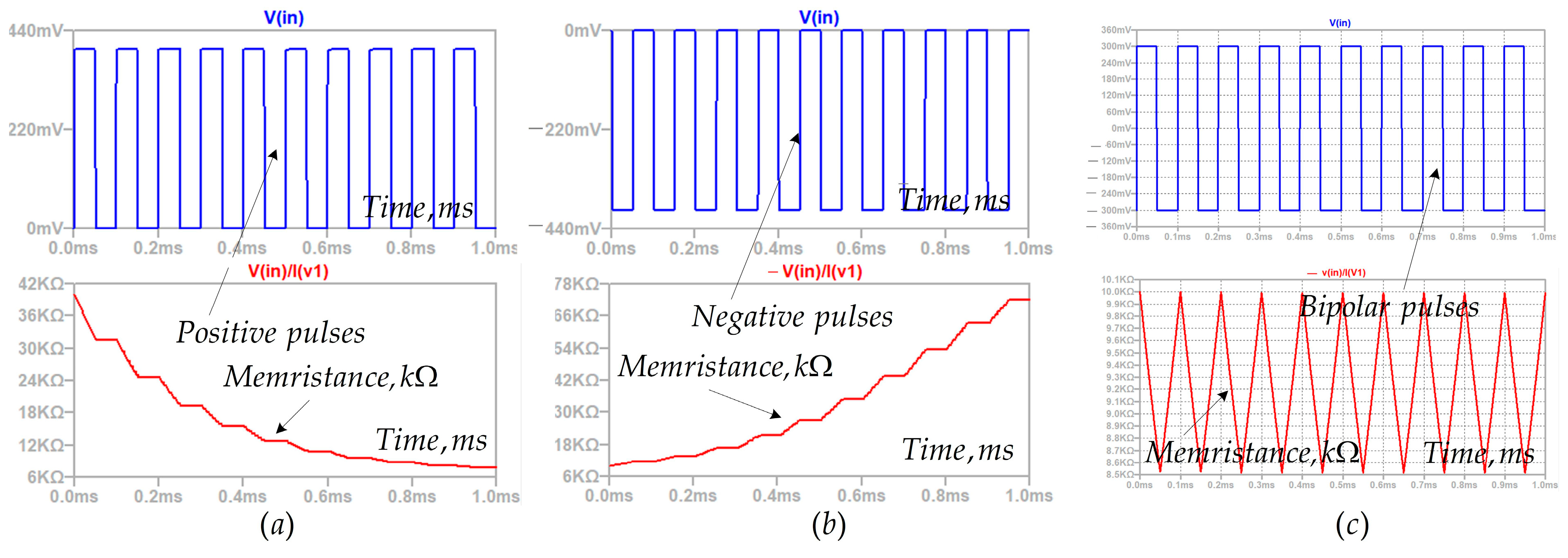
The alteration of memristance at applied positive impulse voltage is represented in Figure 5a. It is visible that during the impulses, the memristance decreases. During the pauses, the memristance has a constant value. The observed phenomenon is related to the memory effect. The results obtained from the analysis of the memristor model at negative voltage pulses are presented in Figure 5b. During the pulses, the memristance increases. The proposed memristor model is tested at bipolar pulses as well. The derived results are presented in Figure 5c.
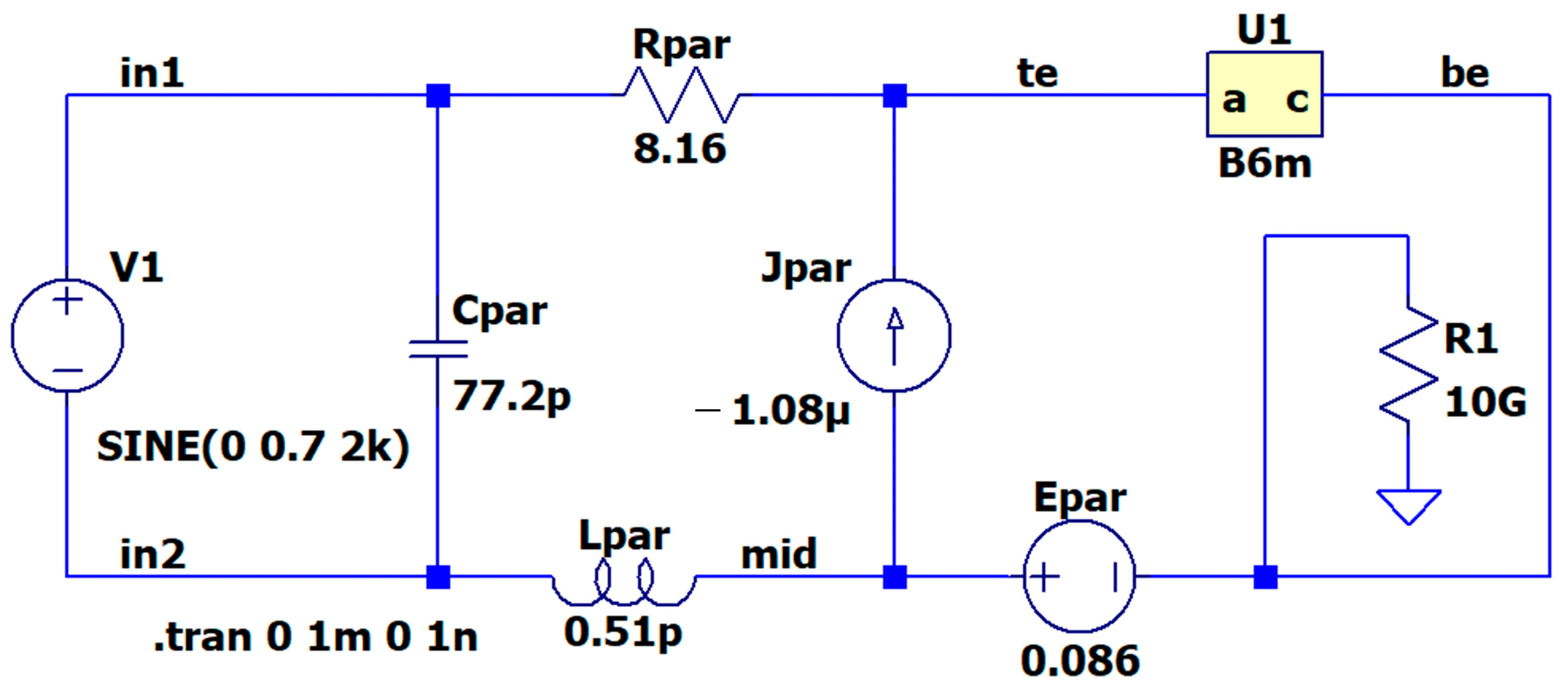
The proposed LTSPICE memristor model with parasitic parameters is denoted as B6par. It is based on the previously discussed memristor model B6m and the discussed parasitic parameters—resistance, inductance, capacitance, and the small-signal DC voltage and current components. The equivalent schematic of model B6par in LTSPICE simulator is presented in Figure 6. It corresponds to the principal schematic of this modified memristor model, as presented in Figure 1a.
The LTSPICE code, corresponding to Figure 6, is presented below. The terminals of the memristor are denoted as in1 and in2. The parasitic capacitance Cpar is connected between these terminals. The structure of the code corresponds to the schematic presented in Figure 6 and Formula (4). For generation of the circuit element, corresponding to the described LTSPICE code, the interested readers should first create the memristor model B6m.
Additional and detailed explanations about generation of the respective LTSPICE circuit elements are presented at the following link:
9.
.subckt b6par in1 in2
10.
Cpar in1 in2 77.2p
11.
Rpar te in1 8.16
12.
Lpar mid in2 0.51p
13.
I§Jpar mid te −1.08µ
14.
V§Epar mid be 0.086
15.
XU1 te be B6m
16.
R1 be 0 10G
17.
.lib C:\Users\StoyanKirilov\Desktop\LTSPICE_MODELS\b6m.cir
18.
.backanno
19.
.ends b6par
Figure 7 presents a short comparison between the proposed memristor models B6m and B6par, according to the basic characteristics of the memristors. Figure 7a–c are related to simulations of these memristor models at sine-wave signals at a given amplitude and different frequencies. At the low frequency of 2 kHz, their behavior is almost identical. At 10 kHz and 20 kHz, the current–voltage relations are quite different one to another, owing to the influence of the parasitic inductance and capacitance.
The analyses conducted at pulse signals are presented in Figure 8a–c. It is visible that the parasitic parameters affect the memory and commutating properties of the memristors. Memory properties are very important during the adjustment of synaptic weights in memristor-based neural networks.

4. The Suggested Memristor-Based Artificial Neuron

In this Section, the organization and functioning of the suggested memristor-based artificial neuron are described and commented.

4.1. The Structure of a Simple Memristor-Based Artificial Neuron

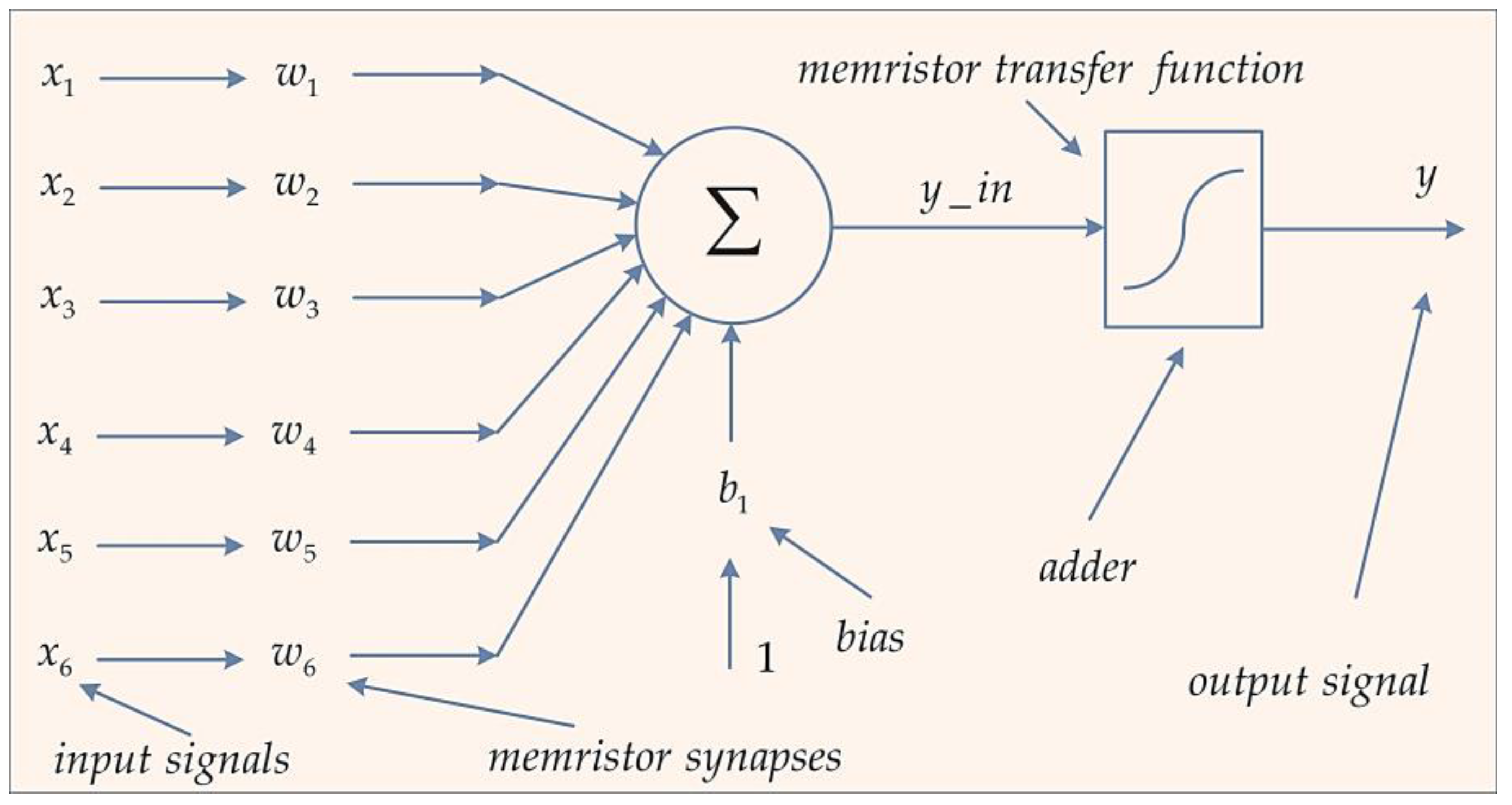
A block scheme of an artificial memristor-based neuron is presented in Figure 9 for visualization of its basic structure and functioning. The input signals are denoted as x1, x2, x3, x4, x5, and x6. The bias signal has a value of unity.
These signals are forwarded to the memristor-based synaptic weights, represented as w1, w2, w3, w4, w5, and w6. The bias weight is denoted as b1. Each synaptic weight is realized by a single memristor, whose conductance determines the synaptic weight. The signals after the synaptic weights are directed to an adder, which is realized with memristors and op-amps [6]. The output signal of the adder is denoted as y_in. This signal is applied to the input of a modified tangent-sigmoidal activation function, based on memristors and MOS transistors. The output signal of the memristor neuron is expressed as y. The operation of the commented memristor-based artificial neuron is based on feed-forward transfer of input signal and back-error propagation algorithm for updating the synaptic weights [6].

4.2. The Realization of Memristor Adder and Synaptic Connections

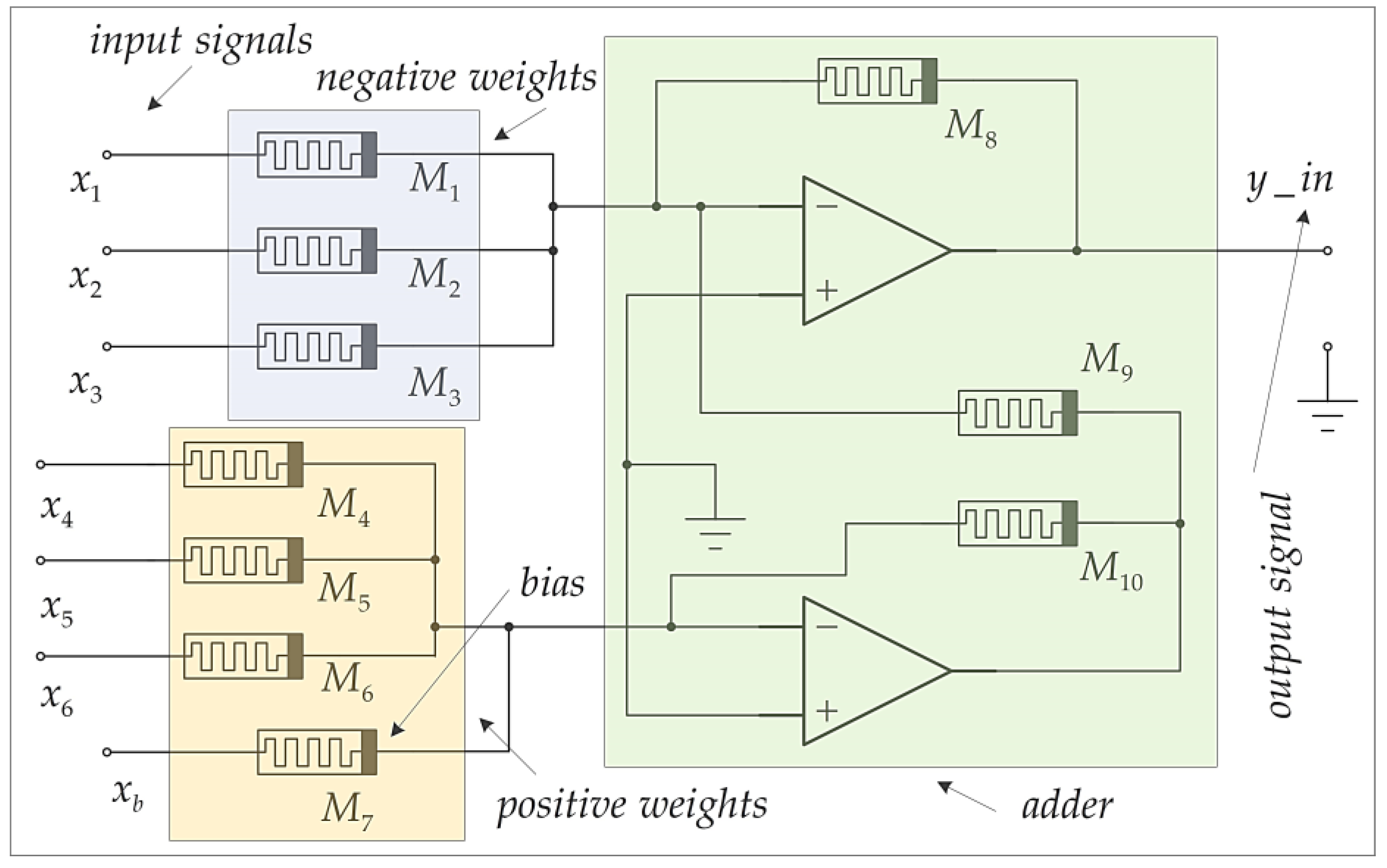
A principal scheme of the synaptic connections and the adder of the memristor-based neuron under analysis is presented in Figure 10 for further discussion. The memristors M1, M2, and M3 are related to negative synaptic weights, and memristors M4, M5, M6, and M7 ensure positive weights [6]. The element M7 realizes the bias of the neuron. The resistances of the memristors M8, M9, and M10 are constants, with a value of 10 kΩ. They could be replaced by linear and simple resistors. The memristors M8 and M10 ensure the feedback for the applied op-amps. The connection between the used op-amps is realized with the memristor element M9.
Utilizing Kirchhoff’s laws (KCL and KVL), and bearing in mind that M8 = M9 = M10, the output signal of the adder y_in is derived [6]:
y i n = M 8 M 1 x 1 M 8 M 2 x 2 M 8 M 3 x 3 + M 10 M 4 x 4 + M 10 M 5 x 5 + M 10 M 6 x 6 + M 10 M 7 x b
The coefficients in front of the signals in (5) represent the synaptic weights:
w 1 = M 8 M 1 ;   w 2 = M 8 M 2 ;   w 3 = M 8 M 3 ;   w 4 = M 10 M 4 ;   w 5 = M 10 M 5 ;   w 6 = M 10 M 6 ;   b 1 = M 10 M 7

4.3. Synaptic Weights Adjustment

The process of synaptic weights tuning is realized by applying external voltage pulses, directed to the respective memristor [3,6]. Let us assume that the applied pulses for adjustment are at a level higher than the activation threshold vthr. Then, from (3), the following state differential Equation (7) could be obtained:
d x d t = x ˙ = η · k · v m e m 3 · x 1 x
After separating the memristor state variable x and the time variable t, the next differential Equation (8) is derived:
d x x 1 x = η · k · v m e m 3 · d t
When the initial value of the memristor state is x1, then its alteration to a new value x2 is obtained for the voltage pulse duration Tmax, according to the following equation:
x min x max 1 x 1 x d x = η · k · v m e m 3 · 0 T max d t = k · v m e m 3 · T max
The needed pulse duration Tmax is expressed after solving Equation (9). It is represented by the following formula:
T max = ln x max + ln 1 x min ln x min ln 1 x max η k v 3
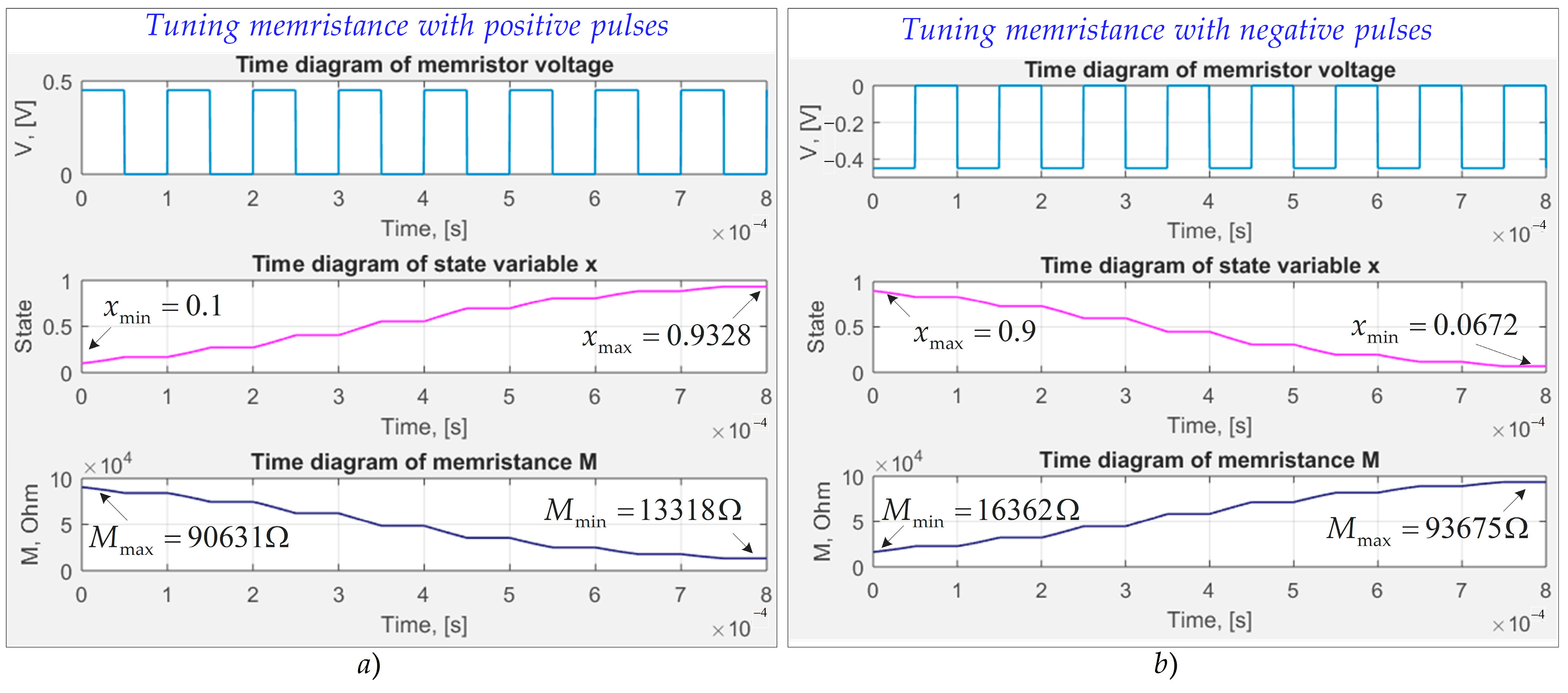
The process of tuning the weights of memristor synapses by voltage impulses is represented in Figure 11. Figure 11a is derived at positive voltage pulses, and Figure 11b is obtained for negative pulses, respectively. The applied sequence of positive pulses leads to decremented memristance and increasing the state variable, respectively. Incremental memristance and decrease in the memristor state variable are obtained at negative voltage impulses. In both incremental and decremented memristances, the pulses are with a duration of 50 µs and a level of 0.45 V. The pulse sequence is with a duty cycle of 50%.
A comparison of the results derived by formula (10) and the simulation results from Figure 11 is conducted. In the case of applied positive voltage pulses, let the initial state variable have a value of xmin = 0.1. It corresponds to a memristance with a value of Mmax = 90631 Ω. The respective synaptic weight is w1 = 10,000/Mmax = 0.1103. According to Figure 11a, the final value of the state variable is xmax = 0.9328, corresponding to a memristance with a value of Mmin = 13,318 Ω. The corresponding synaptic weight is w2 = 10,000/Mmin = 0.7509.
The analytical calculation of the needed effective duration of the applied pulses with a level of 0.45 V is:
T max = ln 0.9328 + ln 1 0.1 ln 0.1 ln 1 0.9328 1 · 132440 · 0.45 3 = 400 μ s
After consideration of Figure 11a and bearing in mind that the duty cycle of the pulse sequence is 50%, the same result is derived. Similar results are obtained at negative voltage pulses. A good closeness between the results is established, which confirms the proper operation of the modified memristor model under analysis.

4.4. A Modified Transfer Function, Based on Memristors and MOS Transistors

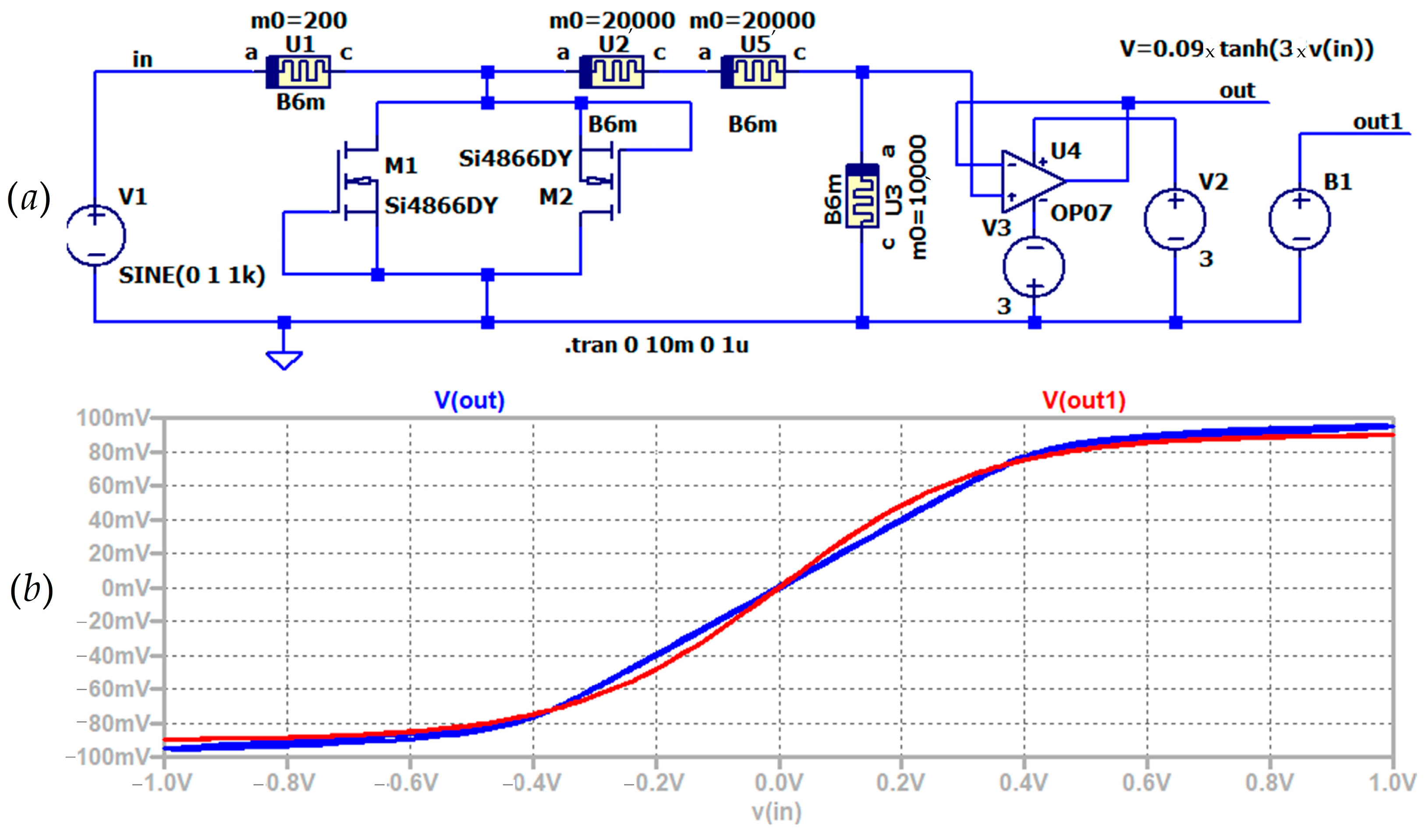
The suggested MOS transistor-memristor activation function is represented with a principal schematic, which is shown in Figure 12. The input signal y_in is forwarded from the output of the previously discussed adder. The memristors M11 and the MOS transistors T1, and T2 conduct a nonlinear conversion on the input signal y_in [6]. The memristors M12 and M13 form a voltage divider, which has a voltage transmission coefficient with a value of 10. The voltage drops across the memristors are lower than the activation threshold, and due to this, these elements behave as linear resistors. The operational amplifier operates as a buffering element. It separates the described transfer function from the next neurons. The circuit presented in Figure 12 realizes a modified tangent-sigmoidal transfer function.
The realization of the above-described modified transfer function in LTSPICE simulator is illustrated in Figure 13a. The input signal could be sinusoidal or impulse one. In the present case, it has the following expression: vout = 0.09 × tanh(3 × vin). It is applied for analysis of the proposed transfer function.
The controlled voltage source B1 is used for representation of an approximate mathematical expression of the modified tangent-sigmoidal function. Its signal “out1” is utilized for comparison with the output signal “out”, which corresponds to the real output signal y. Figure 13b is placed for graphical presentation of the described output signals as functions of the input voltage and for their visual comparison. It is observable that the output signals are very close to one another. The memristors M11, M12, and M13 operate in a linear mode, i.e., these elements are with constant resistance. In some cases, instead of M11, a series connection of memristors could be applied to prevent exceeding the memristor activation threshold vthr [6]. When a memristor operates as a linear resistor, its power consumption is about 3 µW. Otherwise, if it is operating in a soft-switching mode, its power usage is between 30 µW and 3 mW.
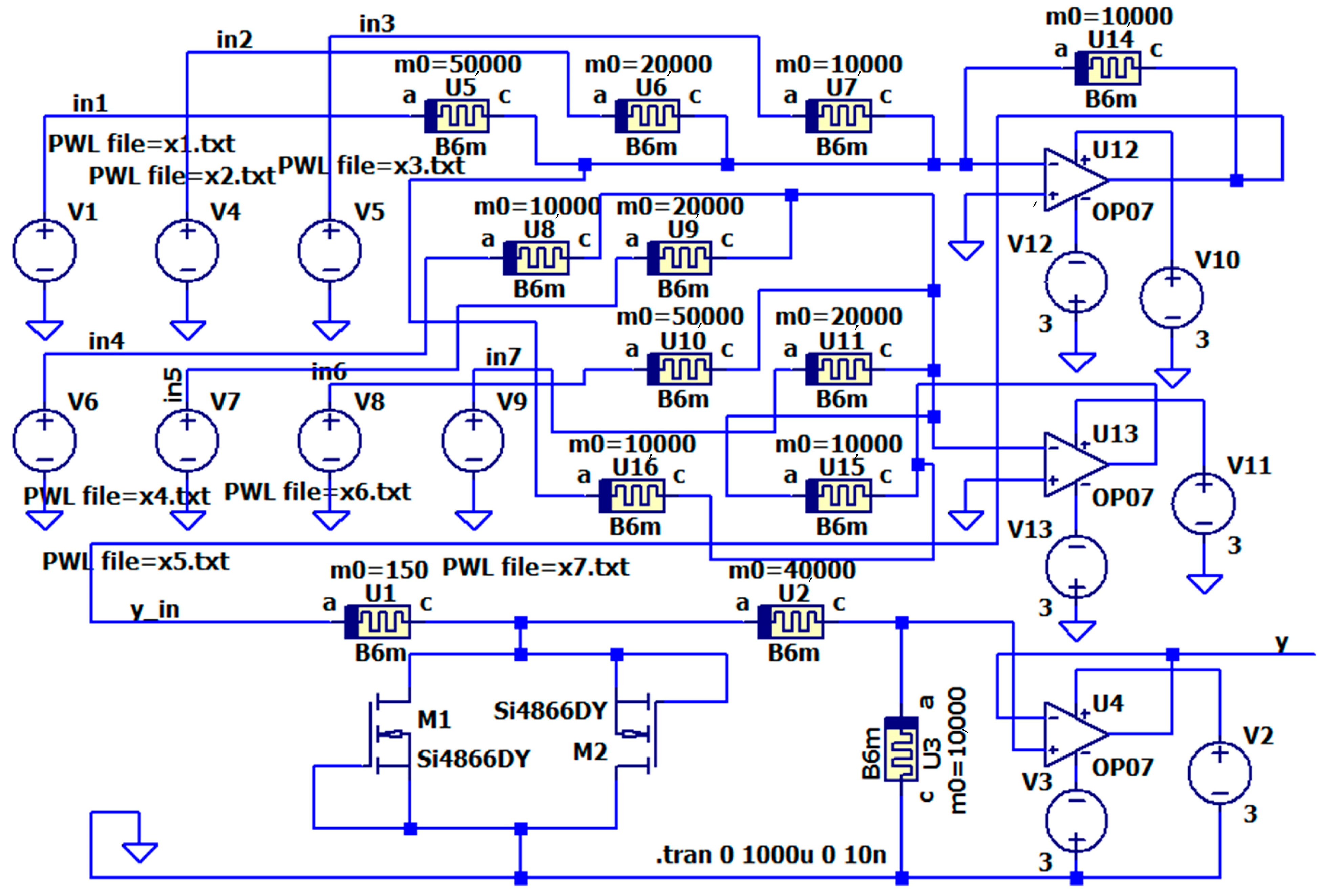
Based on the commented modules, a memristor-based artificial neuron is created and analyzed in the LTSPICE simulator. The corresponding scheme is represented in Figure 10 for further discussion. The voltage sources v1v6 and vb ensure the input signals x1x6 and xb. They are represented by sequences of pulses with different levels.
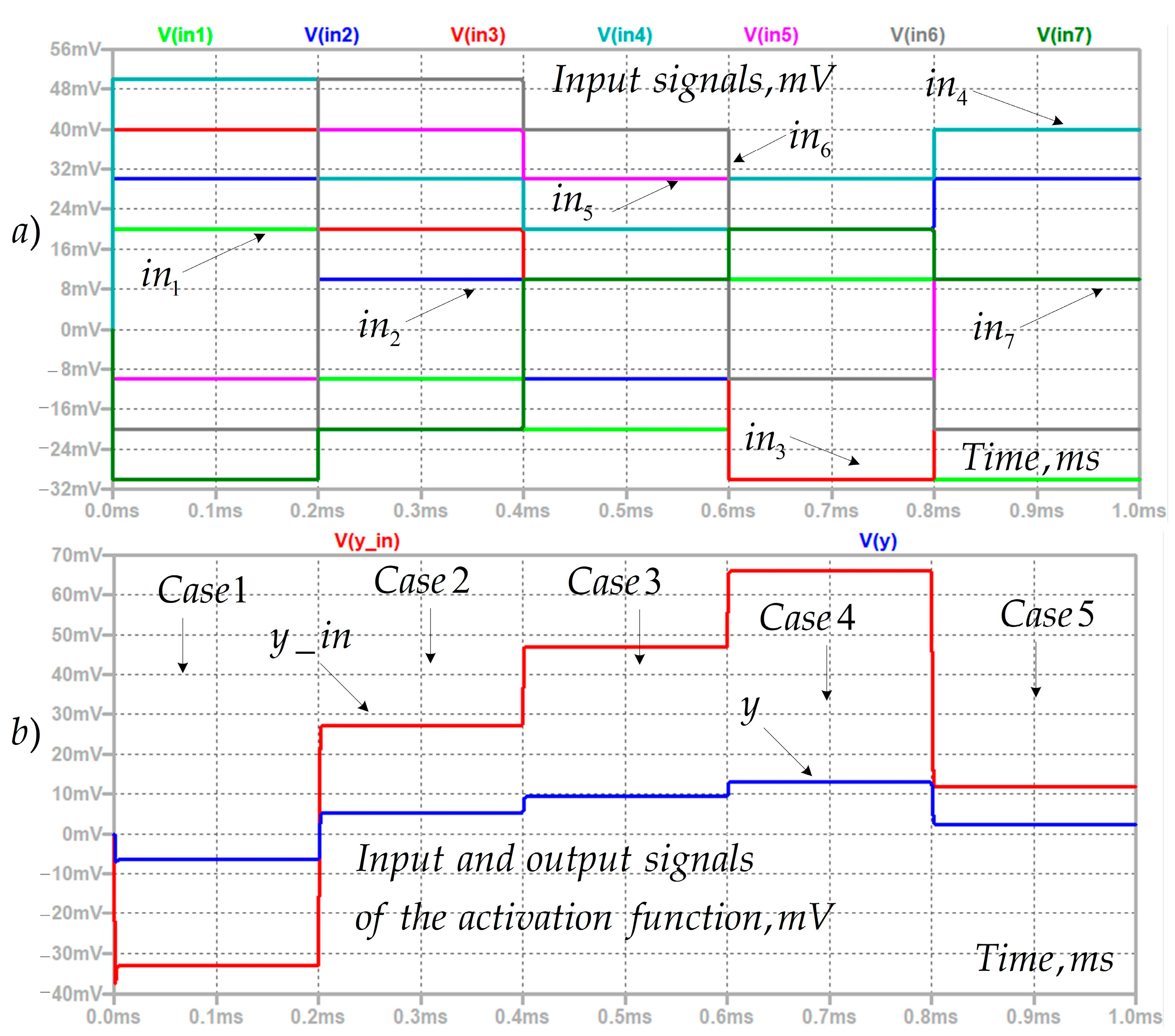
Table 1 represents the levels of the input signals for five different cases.
The synaptic weights and corresponding memristances, which are applied for analysis of the suggested memristor neuron in the MATLAB [23,24], Simulink, and LTSPICE simulators, are shown in Table 2.
Figure 13a presents a schematic of the proposed transfer function. Figure 13b represents the input and the output signals of the modified transfer function.
Figure 14 presents the realization of the proposed memristor-based neuron in LTSPICE.
The applied LTSPICE memristor and neuron models are uploaded and available for use at the link: https://github.com/mladenovvaleri/Advanced-Memristor-Modeling-in-LTSpise [11] (accessed on 12 August 2025).
The time diagrams of the input and output signals of the neuron in LTSPICE are presented in Figure 15a,b.

5. Comparison and Analysis of Derived Results

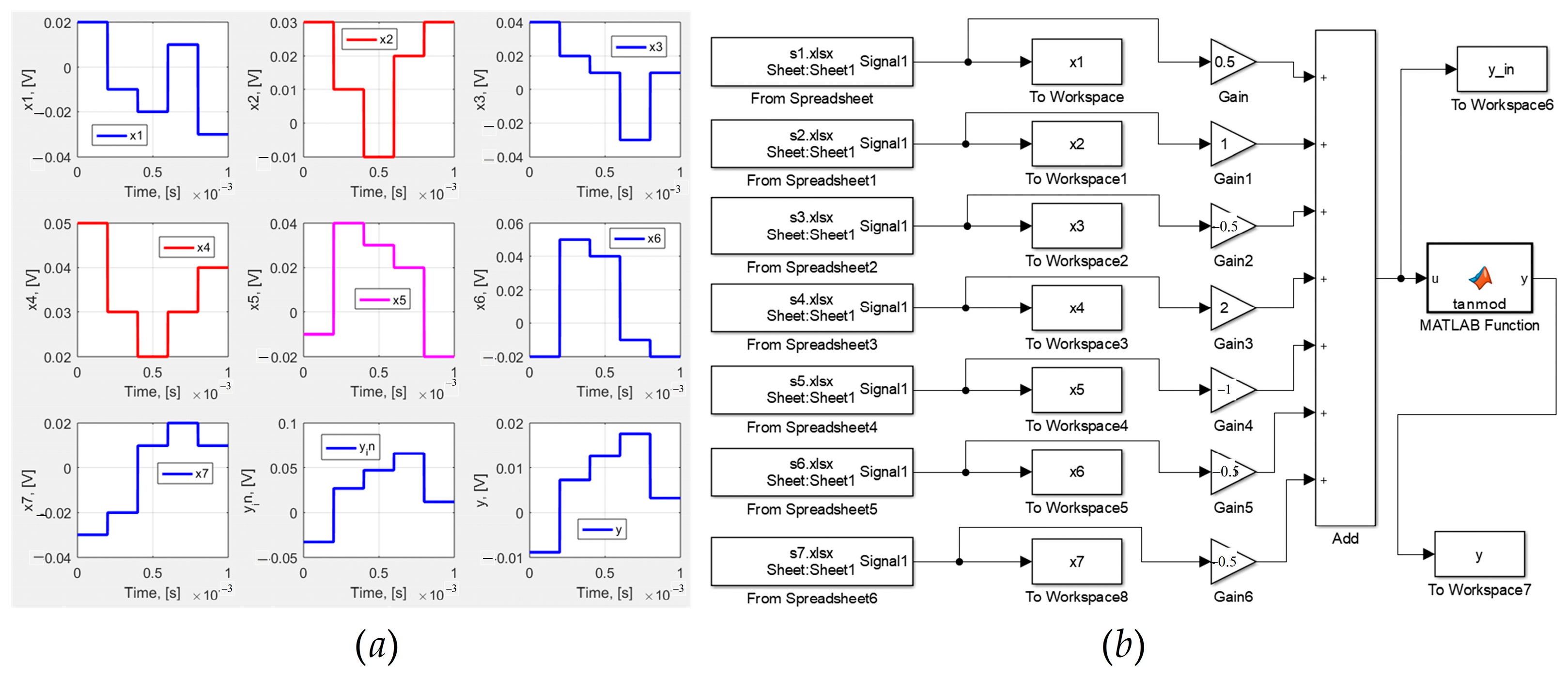
In this Section, a comparison of results, derived in the MATLAB, Simulink, and LTSPICE analyses of the suggested memristor-based neuron is shown and commented. The derived results, according to the time diagrams of the input and output signals of the neuron in Simulink are presented in Figure 16a. The corresponding schematic in Simulink is presented in Figure 16b.
The sources for input signals are of type “From spreadsheet”. The synaptic weights are presented with “Gain” elements. The modified transfer function is presented with a “MATLAB function” block in the Simulink environment.

A Comparison of the Results Derived in MATLAB–Simulink and LTSPICE

A short comparison of the results, obtained in MATLAB–Simulink and LTSPICE software, is represented in Table 3. The average value of the relative error between the output signals is about 3.546%. This low value of the relative error confirms the correct functioning of the suggested memristor-based artificial neuron.
During the process of utilization of the neuron, the parasitic parameters do not significantly affect the signals’ transmission. The influence of the parasitic parameters on the change in the memristances and the respective synaptic weights during their adjustment by pulses is presented in Table 4. In the first and second rows, the initial values of the synaptic weights and the corresponding memristances are presented. A pulse sequence of 10 pulses with a level of 0.4 V, duty cycle of 50%, and a pulse duration of 5 µs is used. For comparison, the considered memristor models B6m and B6par are applied. The derived results, according to the achieved memristances and synaptic weights are placed in the next four rows. It is visible that the error between the synaptic weights is about 4.3%. The conclusion is that for low and middle frequency signals, parasitic parameters do not strongly affect the normal operation of the neuron. For high-frequency signals, parasitic capacitance affects the plateau of the pulses, and it should be taken into account during the weight-adjustment process.

6. Discussion [11,13,16]

During the analyses in MATLAB and LTSpice, the standard Biolek, Lehtonen–Laiho and Knowm memristor models are applied, together with the discussed modified memristor models B6m and B6par. A short comparison of the utilized memristor models is conducted. For this purpose, several significant criteria, such as the model complexity, accuracy, operating frequency, switching properties, and simulation time, are used [11,13,16].
The complexity of a memristor model is proportional to the number of elementary mathematical operations included in the respective system of describing equations [16].
Model’s accuracy is related to its ability for precise representation of the experimentally recorded current–voltage characteristics, with a minimal RMS error [13].
The operating frequency depends on the capability of the memristor model to realistically represent the nonlinear ionic dopant drift at low-, middle-, and high-level signals, ensuring a broad range for alteration of the state variable. Low frequencies are between 1 and 1 kHz, middle frequencies are about 10 kHz, and high frequencies are higher than 10 kHz [11].
The switching properties are related to the ability of a given memristor model to represent the realistic change in the memristance and the respective state variable under applied voltage pulses, for both soft-switching and hard-switching modes [11,16].
Simulation time of a model is related and directly proportional to the complexity of the considered memristor model [11,13].
For analyses and simulations of complex memristor-based circuits, simple, accurate, and fast-operating memristor models are needed [11,16].
The results from the comparison are presented in Table 5 to express the main advantages and disadvantages of the proposed modified memristor models. The proposed modified memristor models are with a comparatively low complexity, high operational frequency, and good accuracy and switching properties. As a little disadvantage of the modified models, their decreased accuracy should be taken into account. They are appropriate for the analysis and simulation of multipart memristor-based circuits and devices.

7. Conclusions

In the end of this paper, it could be concluded that the purpose of the work is achieved, and the related tasks are successfully resolved. Simple, accurate, and fast-operating LTSPICE models of memristors are suggested and applied in the activation function, synapses, and adder for the realization of an artificial neuron. In the applied memristor models, the main and frequently observed parasitic parameters—resistance, inductance, capacitance, and the small-signal DC voltage and current components—are considered. The synaptic connections for positive and negative weights are realized with single memristors and a summing device, implemented with two op-amps. The suggested modified tangent-sigmoidal activation function is based on MOS transistors and memristors. For the conducted analyses and computer simulations, both LTSPICE and MATLAB–Simulink software products are used. The derived results approve the correct operation of the suggested memristor-based neuron. Its main advantages are the simple hardware and software implementations. For its realization, low-power self-directed Knowm memristors with nano-sizes and good compatibility to CMOS integrated chips are applied.
The influence of the parasitic parameters on the normal operations of the memristors at medium and high frequencies is considered mainly during the adjustment of the synaptic weights, as well as during the regime of usage of the memristor neuron. The parasitic parameters and especially the capacitances distort the fronts and plateau of the pulses. The DC voltage and current small-signal sources shift the intersection point of the voltage–current characteristics of the memristors, according to the origin of the Cartesian i-v plane. The ambient temperature also affects the operating mode, but the change in memristor characteristics is very small. The conducted analyses did not expose any serious deviation of the pulse levels from the desired values.
As potential future work on the topic, a more detailed study of the influence of parasitic parameters on the switching and memory properties of the memristors and synaptic weights’ alteration in more complex neural networks is planned, focusing on the extent and significance of the influence of parasitic parameters on the normal operation of neuron and neural networks. The limited bandwidth of the operational amplifiers could also be analyzed, together with some nonlinear relations between the parasitic capacitance and the voltage.
The suggested realization of an artificial memristor-based neuron is a significant step toward novel and high-density neuromorphic electronic circuits and devices.

Author Contributions

Conceptualization, V.M. and S.K.; methodology, V.M. and S.K.; software, V.M. and S.K.; validation, V.M. and S.K.; formal analysis, V.M.; investigation, V.M. and S.K.; resources, V.M. and S.K.; data curation, V.M. and S.K.; writing—original draft preparation, V.M. and S.K.; writing—review and editing, V.M.; visualization, V.M.; supervision, V.M.; project administration, V.M. All authors have read and agreed to the published version of the manuscript.

Funding

This research received no external funding.

Data Availability Statement

The original contributions presented in this study are included in the article. Further inquiries can be directed to the corresponding author.

Conflicts of Interest

The authors declare no conflicts of interest.

Abbreviations

The following abbreviations are used in this manuscript:
MOSMetal-Oxide Semiconductor Transistor
CMOSComplementary Metal-Oxide Semiconductor Technologies
KCLKirchhoff Current Law
KVLKirchhoff Voltage Law
SPICESimulation Program with Integrated Circuits Emphasis
LTspiceLinear Technology SPICE software
MATLABMATrix LABoratory software
RAMRandom Access Memory
SSDSolid-State Disk Drive
RMSERoot Mean Square Error
CADComputer-Aided Design Software
DCDirect Current components
AIArtificial Intelligence

References

  1. Aggarwal, C. Neural Networks and Deep Learning; Springer International Publishing AG: Berlin/Heidelberg, Germany, 2018; p. 497. ISBN 978-3-319-94463-0. [Google Scholar]
  2. Xu, W.; Wang, J.; Yan, X. Advances in memristor-based neural networks. Front. Nanotechnol. 2021, 3, 645995. [Google Scholar] [CrossRef]
  3. Hong, Q.; Zhao, L.; Wang, X. Novel circuit designs of memristor synapse and neuron. Neurocomputing 2019, 330, 11–16. [Google Scholar] [CrossRef]
  4. Wang, S.; Song, L.; Chen, W.; Wang, G.; Hao, E.; Li, C.; Hu, Y.; Pan, Y.; Nathan, A.; Hu, G.; et al. Memristor-Based Intelligent Human-Like Neural Computing. Adv. Electron. Mater. 2023, 9, 2200877. [Google Scholar] [CrossRef]
  5. Strukov, D.B.; Snider, G.S.; Stewart, D.R.; Williams, S. The missing memristor found. Nature 2008, 453, 80–83. [Google Scholar] [CrossRef] [PubMed]
  6. Kirilov, S.; Mladenov, V. A Simple LTSPICE Memristor Neuron with a Modified Transfer Function. In Proceedings of the 2024 13th International Conference on Modern Circuits and Systems Technologies (MOCAST), Sofia, Bulgaria, 28–30 June 2024; pp. 1–4. [Google Scholar] [CrossRef]
  7. Adhikari, S.P.; Yang, C.; Kim, H.; Chua, L.O. Memristor bridge synapse-based neural network and its learning. IEEE Trans. Neural Netw. Learn. Syst. 2012, 23, 1426–1435. [Google Scholar] [CrossRef] [PubMed]
  8. Wen, S.; Xie, X.; Yan, Z.; Huang, T.; Zeng, Z. General memristor with applications in multilayer neural networks. Neural Netw. 2018, 103, 142–149. [Google Scholar] [CrossRef] [PubMed]
  9. Biolek, Z.; Biolek, D.; Biolkova, V. SPICE Model of Memristor with Nonlinear Dopant Drift. Radioengineering 2009, 18, 210–214. [Google Scholar]
  10. Kolka, Z.; Biolkova, V.; Biolek, D. Simplified SPICE model of TiO2 Memristor. In Proceedings of the International Conference MEMRISYS, Paphos, Cyprus, 8–10 November 2015; pp. 1–2. [Google Scholar]
  11. Mladenov, V. A Unified and Open LTSPICE Memristor Model Library. MDPI Electron. 2021, 10, 1594. [Google Scholar] [CrossRef]
  12. Solovyeva, E.B.; Azarov, V.A. Comparative Analysis of Memristor Models with a Window Function Described in LTspice. In Proceedings of the 2021 IEEE Conference of Russian Young Researchers in Electrical and Electronic Engineering (ElConRus), Moscow, Russia, 26–29 January 2021; pp. 1097–1101. [Google Scholar]
  13. Dautovic, S.; Samardzic, N.; Juhas, A.; Ascoli, A.; Tetzlaff, R. Simscape and LTspice models of HP ideal generic memristor based on finite closed form solution for window functions. In Proceedings of the 2021 ICECS Conference, Dubai, United Arab Emirates, 28 November–1 December 2021; pp. 1–6. [Google Scholar]
  14. Sah, M.P.; Yang, C.; Kim, H.; Muthuswamy, B.; Jevtic, J.; Chua, L. A generic model of memristors with parasitic components. IEEE Trans. Circuits Syst. 2015, 62, 891–898. [Google Scholar] [CrossRef]
  15. Tsenov, G.T.; Kirilov, S.; Mladenov, V. SPICE memristor model based on estimate from measured data. COMPEL—Int. J. Comput. Math. Electr. Electron. Eng. [CrossRef]
  16. Ascoli, A.; Tetzlaff, R.; Biolek, Z.; Kolka, Z.; Biolkova, V.; Biolek, D. The Art of Finding Accurate Memristor Model Solutions. IEEE J. Emerg. Sel. Top. Circ. Syst. 2015, 5, 133–142. [Google Scholar] [CrossRef]
  17. Fares, D.A.; Joujou, M.K.; Khaddaj, S.I.; Kabalan, K.Y. A learning approach to circuitry problems using MATLAB and PSPICE. In Proceedings of the 2012 IEEE Global Engineering Education Conference (EDUCON), Marrakech, Morocco, 17–20 April 2012; pp. 1–5. [Google Scholar] [CrossRef]
  18. Campbell, K.A. Self-directed channel memristor for high temperature operation. Microelectron. J. 2017, 59, 10–14. [Google Scholar] [CrossRef]
  19. Bednarz, K.; Garda, B. Measurement and Modeling of Self-Directed Channel (SDC) Memristors: An Extensive Study. Energies 2017, 17, 5400. [Google Scholar] [CrossRef]
  20. Lehtonen, E.; Laiho, M. CNN using memristors for neighborhood connections. In Proceeding of the Conference CNNA, Berkeley, CA, USA, 3–5 February 2010; pp. 1–4. [Google Scholar]
  21. Joglekar, Y.N.; Wolf, S.J. The elusive memristor: Properties of basic electrical circuits. Eur. J. Phys. 2009, 30, 661. [Google Scholar] [CrossRef]
  22. Prodromakis, T.; Peh, B.P.; Papavassiliou, C.; Toumazou, C. A versatile memristor model with nonlinear dopant kinetics. IEEE Trans. Electron Devices 2011, 58, 3099–3105. [Google Scholar] [CrossRef]
  23. Kharab, A.; Guenther, R. An Introduction to Numerical Methods: A MATLAB® Approach; CRC Press: Boca Raton, FL, USA, 2018; p. 631. ISBN 9781315107042. [Google Scholar] [CrossRef]
  24. Kim, P. Matlab Deep Learning. In With Machine Learning, Neural Networks and Artificial Intelligence; APress: New York, NY, USA, 2017; ISBN 978-14842-28456. [Google Scholar]
  25. Zhevnenko, D.A.; Meshchaninov, F.P.; Kozhevnikov, V.S.; Shamin, E.S.; Telminov, O.A.; Gornev, E.S. Research and Development of Parameter Extraction Approaches for Memristor Models. Micromachines 2021, 12, 1220. [Google Scholar] [CrossRef] [PubMed]
  26. Shooshtari, M.; Kim, S.Y.; Pahlavan, S.; Rivera-Sierra, G.; Través, M.J.; Serrano-Gotarredona, T.; Bisquert, J.; Linares-Barranco, B. Advancing Logic Circuits With Halide Perovskite Memristors for Next-Generation Digital Systems. SmartMat 2025, 6, e70032. [Google Scholar] [CrossRef]
  27. Slipko, V.A.; Pershin, Y.V.; Di Ventra, M. Changing the state of a memristive system with white noise. Phys. Rev. E—Stat. Nonlinear Soft Matter Phys. 2023, 87, 042103. [Google Scholar] [CrossRef] [PubMed]
  28. Kumar, N.; Han, J.E.; Beckmann, K.; Cady, N.; Sambandamurthy, G. Noise Spectroscopy and Electrical Transport In NbO2 Memristors with Dual Resistive Switching. Adv. Electron. Mater. 2025, 11, 2400877. [Google Scholar] [CrossRef]
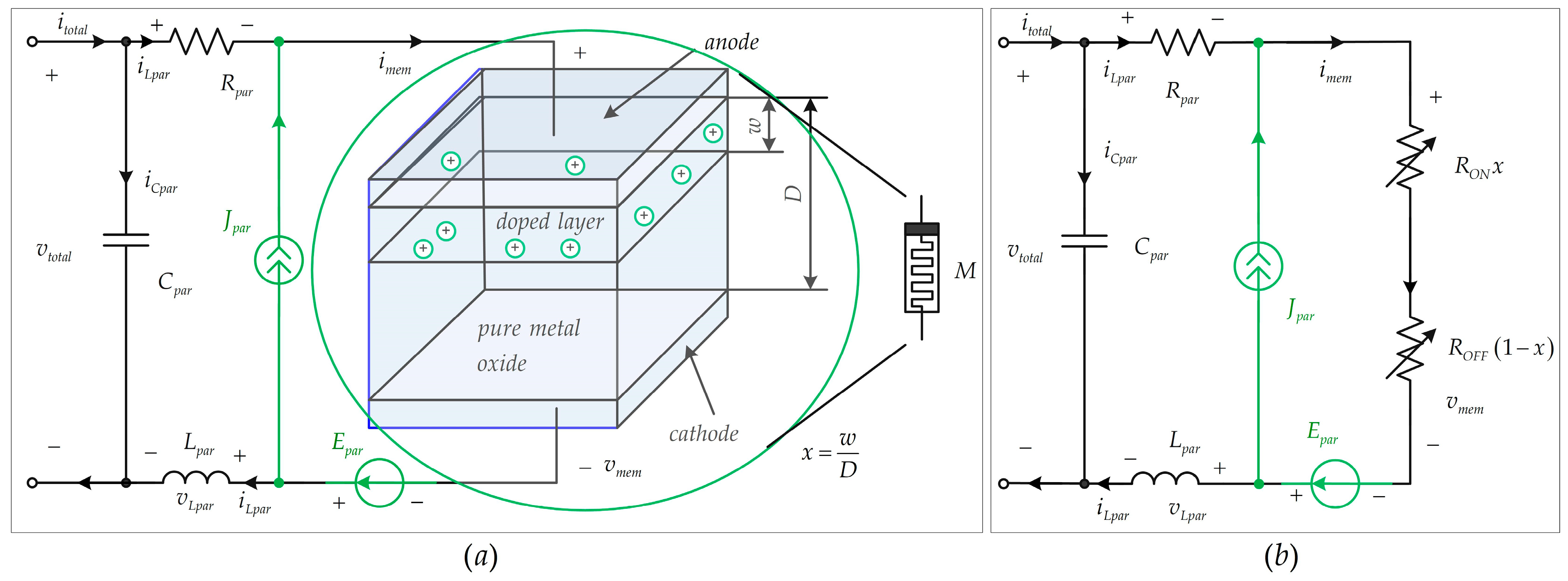
Figure 1. (a) A simple illustration of a metal-oxide memristor nanostructure, including the parasitic parameters—resistance, inductance, capacitance, and small-signal DC voltage and current sources [14]; (b) equivalent circuit of a metal-oxide memristor with the parasitic parameters.
Electronics 14 04645 g001
Figure 2. (a) Experimental schematic for measurement of i-v relations of Knowm memristors; (b) a principal schematic of the experimental setup, including a limiting resistor R = 10 kΩ and a 4-channel digital oscilloscope with a maximal frequency of 100 MHz, sampling frequency of 1 GHz, resolution of 1 ns in time domain and 2 mV/div for applied voltage signals, at sine-wave signal with a frequency of 10 kHz.
Electronics 14 04645 g002
Figure 3. (a) Normalized values of model’s parameters and their trajectories during the estimation process; (b) time diagrams of memristor voltage, state variable, and experimental and simulated memristor currents after parameter estimation procedure; (c) current–voltage relations—experimental and simulated curves of the adjusted memristor model B6par and the corresponding model’s parameters.
Electronics 14 04645 g003
Figure 4. Current–voltage relations of the proposed memristor model B6m obtained at sine mode and various frequencies: (a) f = 5 kHz; (b) f = 20 kHz; (c) f = 100 kHz.
Electronics 14 04645 g004
Figure 5. Operation of memristor model B6m in pulse modes: (a) at positive impulses, (b) at negative pulses, and (c) operation of the proposed memristor model at bipolar pulses.
Electronics 14 04645 g005
Figure 6. LTSPICE equivalent schematic of the proposed memristor model with parasitic parameters B6par.
Electronics 14 04645 g006
Figure 7. A comparison of the proposed memristor models B6m and B6par at sine-wave mode with a given amplitude and different frequencies: (a) f = 2 kHz; (b) f = 10 kHz; (c) f = 20 kHz.
Electronics 14 04645 g007
Figure 8. A comparison of the proposed memristor models B6m and B6par at pulse mode: (a) at positive pulses; (b) at negative pulses; (c) at bipolar pulses.
Electronics 14 04645 g008
Figure 9. A block scheme of a memristor-based artificial neuron.
Electronics 14 04645 g009
Figure 10. A principal scheme of the memristor-based synaptic connections and the adder.
Electronics 14 04645 g010
Figure 11. (a) Tuning the synaptic weights by positive voltage pulses; (b) adjustment with negative voltage pulses.
Electronics 14 04645 g011
Figure 12. A principal scheme of the suggested modified memristor-based activation function.
Electronics 14 04645 g012
Figure 13. (a) A modified tangent-sigmoidal activation function in LTSPICE, based on MOS transistors and memristors; (b) a comparison of the derived transfer function with a voltage-controlled source, generating an output signal vout = 0.09 × tanh(3 × vin).
Electronics 14 04645 g013
Figure 14. Realization of a memristor-based neuron with a modified tangent-sigmoidal transfer function in LTSPICE electronic simulator.
Electronics 14 04645 g014
Figure 15. (a) Time diagrams of the input signals of the memristor neuron in LTspice; (b) time diagrams of the input and the output signals of the transfer function for five different cases.
Electronics 14 04645 g015
Figure 16. (a) Time diagrams of the input and output signals of the memristor-based neuron; (b) a Simulink model of the suggested memristor neuron.
Electronics 14 04645 g016
Table 1. Input signal levels for the memristor neuron for five cases.
Casevin1, mVvin2, mVvin3, mVvin4, mVvin5, mVvin6, mVvb, mV
I20304050−10−20−30
II−101020304050−20
III−20−101020304010
IV1020−303020−1020
V−30301040−20−2010
Table 2. Synaptic weights and corresponding memristances, M7 = M8 = M9 = 10 kΩ.
Synapse1234567
Weight−0.2−0.5−110.50.20.5
M, kΩ50201010205020
Table 3. Input and output signals of the neuron from MATLAB–Simulink and LTSPICE.
CaseY_in MATLAB–Simulink mVY_in LTSpice mVRelative Error Between Y_in MATLAB and Y_in LTSPICE, %Y MATLAB–Simulink, mVY LTSpice mVRelative Error Between Y MATLAB and Y_in LTSPICE, %
I−33−33.030.091−8.88−8.573.49
II3737.41.087.277.41.79
III4747012.611.895.63
IV6666017.617.162.5
V12.2121.673.243.14.32
Table 4. Influence of the parasitic parameters on the adjustment of synaptic weights and memristances.
Synapse1234567
Initial values of the synaptic weights−0.2−0.5−110.50.20.5
Initial values of the memristances, kΩ50201010205020
Weights achieved according to model B6m−0.23−0.68−1.451.450.680.230.68
Memristances according to model B6m, kΩ43.914.66.96.914.643.914.6
Weights achieved according to model B6par−0.21−0.52−1.521.520.520.210.52
Memristances according to model B6par, kΩ47.819.16.66.619.147.819.1
Table 5. A comparison of the memristor models under analysis [11].
Memristor ModelComplexityAccuracyOperating FrequencySwitching PropertiesSimulation Time
K3 [9]lowaverageaveragesatisfactory14.7 ms
K5 [20]highhighhighgood17.2 ms
Knowm [18,19]highhighhighgood17.9 ms
B6m [6]lowhighhighgood16.1 ms
B6parhighaverageaveragesatisfactory17.7 ms
Disclaimer/Publisher’s Note: The statements, opinions and data contained in all publications are solely those of the individual author(s) and contributor(s) and not of MDPI and/or the editor(s). MDPI and/or the editor(s) disclaim responsibility for any injury to people or property resulting from any ideas, methods, instructions or products referred to in the content.