Abstract
The performance bottleneck arising from the speed disparity between the CPU and DRAM highlights the inherent limitations of the von Neumann architecture. To address this issue, we propose a PIM architecture based on a 2T DRAM structure. The proposed PIM design performs Boolean operations directly within the 2T DRAM array, thereby minimizing data movement between the CPU and DRAM and effectively alleviating the bottleneck. The 2T DRAM array was implemented using the mixed-mode simulation capability of SILVACO TCAD, and its read, write, and hold operations were successfully verified. Building on this foundation, OR and AND logic operations were realized by modulating the gate voltages of MOSFETs within the 2T DRAM array. To enable XNOR functionality, an auxiliary circuit consisting of three additional MOSFETs was integrated. Furthermore, as the ultimate goal of PIM is to enable memory to perform computational tasks, support for MAC operations becomes essential. To facilitate this, we designed a refresh circuit capable of maintaining multi-state data, which is critical for MAC operations. This circuit, also composed of three MOSFETs, functions as a key component for multi-state data retention within the 2T DRAM array. In summary, we demonstrate the implementation of Boolean logic operations using the 2T DRAM array and a three-MOSFET auxiliary circuit and propose a compact refresh circuit to support MAC operations, advancing the potential of PIM architectures.
1. Introduction
The rapid advancement of artificial intelligence (AI), high-performance computing, the Internet of Things (IoT), and big data—collectively regarded as hallmarks of the Fourth Industrial Revolution—has accelerated the demand for efficient data processing and analysis. In particular, AI and big data applications necessitate exceptionally high computational throughput. To address these requirements, dynamic random-access memory (DRAM), which serves as the primary system memory, has been scaled toward higher densities and improved operating speeds. Nevertheless, DRAM continues to lag behind central processing units (CPUs) in terms of access latency. Whereas CPU operations are executed on the order of a few nanoseconds, DRAM access typically requires several tens of nanoseconds. This latency disparity gives rise to the well-known memory wall problem, whereby the CPU is forced to idle while awaiting data transfers from main memory, ultimately degrading overall system performance (Figure 1) [1,2,3,4,5,6]. To mitigate this bottleneck, techniques such as cache memory and high-bandwidth memory (HBM) have been introduced. However, these solutions remain constrained by the von Neumann architecture, in which the physical separation of computation and memory inherently necessitates frequent data transfers. Consequently, recent research has shifted toward non–von Neumann paradigms, most notably processing-in-memory (PIM), which aims to reduce data movement by embedding computation within memory structures.
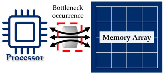
Figure 1.
Memory wall problem diagram. Bottlenecks appear due to differences in operating speed when exchanging data between CPU and memory.
Among memory technologies for PIM implementation, static random-access memory (SRAM) and DRAM are regarded as the most practical options due to their high operating speed and compatibility with large-scale manufacturing. Compared with SRAM, DRAM offers greater potential for reducing PIM cell area and achieving low-power operation (Table 1). Current state-of-the-art neuromorphic processors, such as IBM’s TrueNorth and Intel’s Loihi, are based on SRAM. However, realizing PIM architectures with broad versatility and specialized functionality through multiply–accumulate (MAC) operations requires both high data-processing capability and reduced hardware lightweight. Consequently, the development of DRAM-based PIM technology—combining high speed, low power consumption, and strong scalability—has become increasingly important. In 2015 and 2016, Carnegie Mellon University introduced a method to enable basic logic operations in DRAM arrays by modifying conventional driving schemes. This work demonstrated that operations such as NOT, AND, and OR could be executed directly within DRAM, underscoring its potential for PIM. Nonetheless, this approach suffered from inevitable data corruption caused by simultaneous reads from multiple cells. Providing a dedicated PIM region within the DRAM array has been proposed as a solution, but such an approach compromises integration density. The subsequent introduction of one-transistor dynamic random-access memory (1T-DRAM), a capacitor-less structure, improved integration density but exhibited poor retention characteristics, limiting its practicality for logic-in-memory operations. To address this issue, 2T-DRAM has emerged as a promising alternative. By employing separate read and write transistors, 2T-DRAM prevents data corruption, enhances retention characteristics, and enables more reliable PIM functionality. Moreover, because read operations rely solely on the read transistor, the access speed is comparable to that of SRAM, rendering 2T-DRAM particularly well suited for high-speed PIM applications.

Table 1.
Performance Comparison of highly applicable PIM RAM.
In this study, we propose PIM, two-transistor dynamic random-access memory (2T DRAM)-based architecture designed to alleviate the von Neumann bottleneck. This work focused on developing and verifying methods for implementing read and computational operations in the 2T DRAM array. The proposed scheme embeds simple logic circuits directly within DRAM, utilizing a minimal number of MOSFETs to support in-memory XOR operations. Furthermore, recognizing that MAC operations are indispensable for replacing conventional processor functions—the ultimate objective of PIM—we introduce a multi-state refresh circuit capable of enabling efficient MAC computations [7,8,9,10,11]. To validate the proposed architecture, we first conducted functional simulations to confirm the feasibility of 2T DRAM as a main memory component. A 2T DRAM array was then implemented to perform fundamental AND and OR operations, followed by the design of an XOR circuit employing only three MOSFETs. Finally, we realized a multi-state refresh circuit, also constructed with three MOSFETs, as a critical building block for MAC execution.
In summary, this work presents a 2T DRAM-based PIM framework that mitigates the inherent limitations of the von Neumann architecture by reducing the frequency of CPU–memory data exchanges. Moreover, by introducing a compact multi-state refresh circuit, we demonstrate the feasibility of processor-level functionality within memory, thereby underscoring the potential of PIM as an enabling technology for next-generation computing architectures.
2. 2T DRAM Investigation
Conventional DRAM cells employ a 1T1C architecture, consisting of a single MOSFET and a storage capacitor [12,13,14,15]. Data is stored in the capacitor as electric charge, which serves as the storage element. In contrast, 2T DRAM eliminates the capacitor by adopting a two-transistor (2T) architecture. In this design, the node that would conventionally connect to the capacitor in 1T1C DRAM is instead connected to the gate of a MOSFET. This gate-connected node functions as the charge storage element and is referred to as the storage node (SN) (Figure 2a) [16,17,18,19,20,21,22]. Data storage in the SN of a 2T DRAM cell is facilitated by the write transistor (Write Tr), which directs charges to the SN. Concurrently, the connection between the SN and the gate of the read transistor (Read Tr) allows charge accumulation on the gate capacitance, supporting data retention. Data is written and retained in 2T DRAM by accumulating or releasing charge within the SN. The 2T DRAM cell can also be organized into an array structure analogous to conventional DRAM. As shown in Figure 2b, each cell connects two word lines (WLs) and two bit lines (BLs). Specifically, the write word line (WWL) and write bit line (WBL) facilitate data storage, while the read word line (RWL) and read bit line (RBL) enable data retrieval. This configuration allows the 2T DRAM array to perform both write and read operations without relying on a discrete capacitor, thereby simplifying the cell structure while maintaining memory functionality.
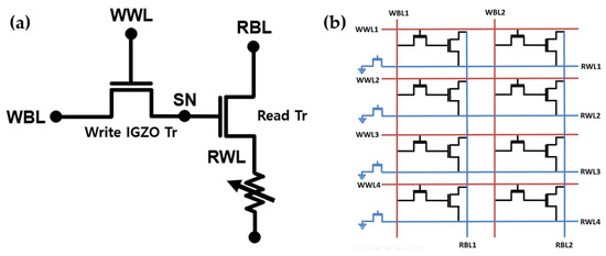
Figure 2.
(a) 2T DRAM cell diagram. Two MOSFETs are connected without a capacitor to implement SN and serve as memory. Data storage in 2T DRAM is achieved by utilizing the gate capacitance of the Read Tr. (b) 2T DRAM array diagram. Two WLs and two BLs are connected to one cell to perform the basic operation of memory.
In 2T DRAM, binary data is written by modulating the charge stored in the storage node (SN) through controlled operation of the write transistor. For a logical “1”, a high voltage is applied simultaneously to the WWL and the WBL, thereby turning on the write transistor. This allows charge to accumulate at the SN, raising its potential and representing a stored “1.” The corresponding voltage conditions and the resulting SN behavior are illustrated in Figure 3a. For a logical “0”, the WWL is driven high to activate the write transistor, while the WBL is maintained at a low voltage. Under these conditions, the previously stored charge in the SN is discharged through the WBL, lowering the node potential and encoding a “0.” Figure 3b depicts the applied voltages and the associated charge dissipation process.
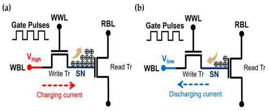
Figure 3.
(a) Diagram in the process of writing data 1. High voltage is applied to the WBL and WWL to store the charge in the SN. (b) Diagram in the process of writing data 0. High voltage is applied to the WWL and low voltage to the WBL to discharge the charge from the SN.
3. 2T DRAM Cell Simulation Results
The 2T DRAM cell was implemented in SILVACO mixed-mode simulation using two MOSFETs, as shown in Figure 4a. The model was applied to the 2T DRAM cell transistor, implemented based on the standard BSIM4 model in PSPICE. Table 2 summarizes the MOSFET model parameters employed for the 2T DRAM cell. Based on these parameters, two MOSFETs were integrated to construct a 2T DRAM cell using mixed-mode simulation. Additionally, the MOSFET bitline (MBL) is connected to the gate of the transistor associated with the read bit line (RBL), while the MOSFET wordline (MWL) is connected to the gate of the transistor associated with the read word line (RWL). Accordingly, the MBL and MWL control the operation of the RBL and RWL, respectively. Core memory functionalities—including write, read, and hold operations—were verified through this implementation. To ensure physical accuracy, the simulations incorporated the Lombardi mobility model, Shockley–Read–Hall (SRH) recombination, and band-to-band tunneling (BTBT) mechanisms. Figure 4b illustrates the timing diagram of the operating voltages applied during write, precharge, and read operations. The diagram depicts the voltage conditions required to store and retrieve a logical “1.” Writing a logical “0” follows the same procedure, except that the WBL is held at a low voltage during the write phase.
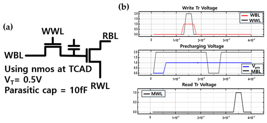
Figure 4.
(a) Implemented 2T DRAM cell diagram. The 2T DRAM cell was implemented by connecting two MOSFETs into one using Mixed mode. (b) 2T DRAM Operation voltage timing diagram. The voltage conditions required for executing the write and read operations of the memory are illustrated. The operating voltage conditions required for the precharge phase prior to data readout are presented.
Table 2.
Conditions of MOSFET Model.
The verification results are summarized in Figure 5. As shown in Figure 5a, when a logical “1” is written, the SN voltage rises and stabilizes at approximately 1 V, confirming successful charge storage and data retention. We measured the retention time of the SN at room temperature (300 K), and the result indicated a retention time of 2.59 s. Figure 5b presents the read operation, in which the SN potential modulates the RBL through the activated read transistor. Specifically, when the RWL is asserted, the RBL voltage decreases in proportion to the SN voltage, thereby enabling accurate data sensing. These results validate the correct functionality of the 2T DRAM cell and confirm its capability to perform fundamental memory operations within the mixed-mode simulation environment.
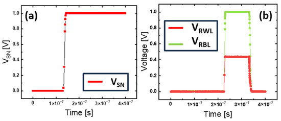
Figure 5.
(a) SN voltage graph after write operation. The voltage variation occurs in proportion to the potentials of the SN and the WBL. (b) Voltage graph of RWL and RBL during read operation. RBL voltage decreases under the influence of SN potential and the RWL, enabling data readout.
4. 2T DRAM Array with Boolean Operation
4.1. Fundamental Boolean Operation
The 2T DRAM cell implemented in mixed mode was extended to an array architecture, as illustrated in Figure 6. To enable selective access, additional MOSFETs were incorporated into the RBL and RWL. Functional verification was performed by addressing individual cells and executing write, read, and hold operations. The results confirmed that the array cells exhibited consistent behavior with the single-cell simulations shown in Figure 4 and Figure 5, thereby demonstrating correct array-level operation.
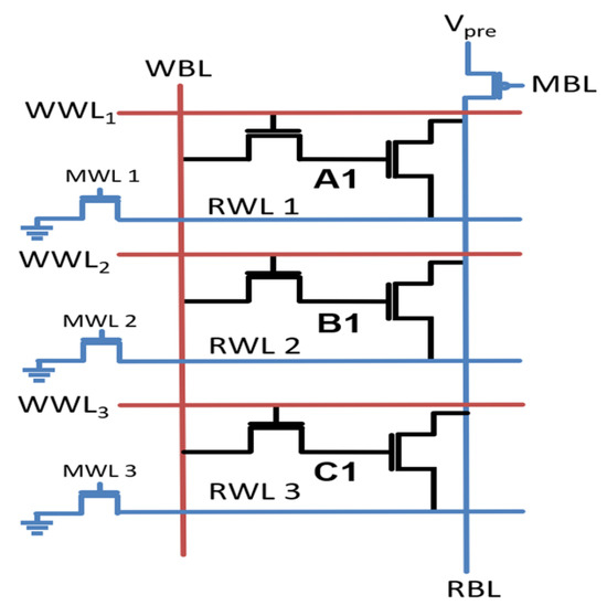
Figure 6.
Implemented 2T DRAM array diagram. The 2T DRAM cell array was implemented in mixed-mode simulation, with additional MOSFETs incorporated to enable cell selection for read operation.
To evaluate in-memory computing capability, Boolean logic operations were implemented within the 2T DRAM array. Test cases were configured by writing binary states into two adjacent cells with input combinations [0,0], [1,0] and [1,1]. Simultaneous read operations were then performed, and the Boolean outputs were determined from the voltage response of the RBL. The RBL is precharged to 1 V prior to the execution of the Boolean operation. Logic functionality was achieved by modulating the gate voltage of the MBL interfaced with the RBL. When a high voltage was applied to the MBL gate (PMOSFET), the circuit performed an OR operation. As shown in Figure 7a, the RBL voltage remained unchanged only in the [0,0] case, while it decreased for [1,0] and [1,1], consistent with OR logic. Conversely, an AND operation was achieved by applying a low voltage to the MBL gate. Figure 7b demonstrates that the RBL voltage is maintained in all input states except [1,1], thereby confirming the AND logic function. Following the AND operation, the voltage of 0.4 V in the [0,0] state is lower than that in the [1,0] state, enabling clear distinction between [1,0] and [0,0]. A sense amplifier is required to unambiguously distinguish the results of the AND operation. With the sensing threshold set to 0.5 V, the output for data [1,1] should be driven from 0.4 V to 0 V, while maintaining clear differentiation of the RBL voltages for [1,0] and [0,0].
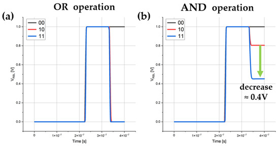
Figure 7.
(a) RBL voltage variation after OR operation. When a high voltage was applied to the MBL, the RBL voltage decreased for all input states except [0,0] (b) RBL voltage variation after AND operation. When a low voltage was applied to the MBL, the RBL voltage increased for all input states except [1,1].
These results demonstrate that both OR and AND operations can be executed directly within the 2T DRAM array by simple gate voltage modulation. The absence of additional circuitry for Boolean operations also enhances the density of 2T DRAM. In particular, OR and AND operations can be selected directly through the gate voltage of the MBL, without the need for prior configuration. This capability highlights the potential of the proposed 2T DRAM architecture to perform PIM, thereby reducing data movement overhead and extending memory functionality beyond conventional storage.
4.2. XOR Boolean Operation Circuit
To enhance the logical functionality of the 2T DRAM array, an additional XOR circuit was introduced, as shown in Figure 8a. The proposed design employs two NMOSFETs and one PMOSFET, with the gates of the transistors coupled to the RBL. In this configuration, the operation state of each device is determined by the RBL voltage. A high bias is applied to the drains of the two transistors connected to the RBL, while the remaining NMOSFET is driven by a high gate voltage with its drain grounded. To ensure that the output is predominantly influenced by the RBL-connected devices, their channel widths were designed to be twice that of the single NMOSFET.
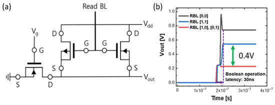
Figure 8.
(a) Peri circuit diagram for XOR operation. The channel widths of the three MOSFETs were intentionally varied to ensure differentiated influence on the XOR circuit output. (b) Vout graph after XOR operation according to four data states. After the XOR operation, the difference in Vout between [1,1] and [1,0] is 0.4 V.
The output characteristics of the XOR circuit under different data states are presented in Figure 8b. For the input combinations 0,0 and 1,1, the circuit produces high-level outputs, whereas for 1,0 and 0,1, the outputs remain at low voltage levels. A voltage margin exceeding 0.4 V was obtained between the high and low states, validating the stable operation of the XOR function. In addition, the latency of the proposed XOR circuit during Boolean operation was measured to be 30 ns, defined as the time between the initiation of the XOR operation and the stabilization of the RBL voltage. Nonetheless, direct current flow from VDD to GND, which is intrinsic to three-state logic operations, poses a potential source of increased power consumption. Accordingly, it is critical to minimize both the current flow and the stabilization time required for the voltage to settle after logical operations. The proposed XOR circuit accomplishes this with a minimal transistor count, thereby preserving the density advantage of the 2T DRAM array. These findings confirm that integrating the XOR circuit with the 2T DRAM array enables direct in-memory execution of Boolean operations, further enhancing the promise of this architecture for PIM applications.
5. Refresh Circuit for Multi-Bit
To enable this functionality, we propose a multi-bit refresh circuit composed of three MOSFETs (Figure 9). The gates of the MOSFETs are connected to the RBL, and their conduction states are determined by the RBL voltage. The output of the circuit is fed back to the WBL of the 2T DRAM array to restore the SN charge. To differentiate device behavior, threshold voltages (Vth) were tuned, and transistor dimensions were scaled: MOSFET B was designed with twice the width of MOSFET A, while MOSFET C was assigned a width more than four times that of A. This sizing strategy ensures that each MOSFET contributes unequally to the output, enabling multi-level refresh functionality.
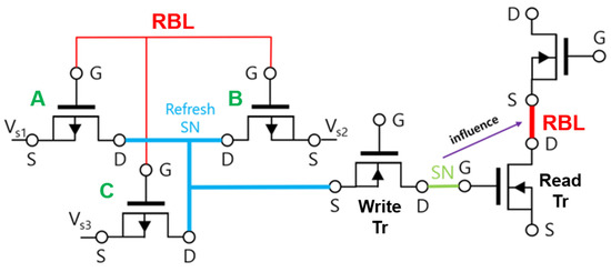
Figure 9.
Multi-bit refresh circuit diagram. The refresh circuit was implemented with three MOSFETs, and the refresh circuit was operated as the voltage of the RBL was affected by the voltage of the SN.
The operation of the refresh circuit proceeds in three stages. First, the SN voltage modulates the resistance of the read transistor, which in turn influences the RBL voltage. Second, the resulting RBL voltage determines the switching state of each MOSFET in the refresh circuit. Finally, the circuit output is generated according to the MOSFET states and applied back to the SN, completing the refresh process. Figure 10a illustrates the SN voltage following refresh as a function of RBL voltage. The circuit maintains a stable output over a defined RBL range, demonstrating tolerance to voltage drift.
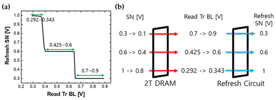
Figure 10.
(a) Graph of change in output of refresh circuit according to RBL. Even if the voltage of the RBL changes between certain sections, the output of the refresh circuit is maintained. (b) Operation flow of multi-bit refresh circuit. The voltage state of the SN gradually varies over time, thereby influencing the RBL voltage. Nevertheless, the refresh circuit maintains a stable output regardless of these RBL voltage fluctuations.
Because the SN voltage in 2T DRAM degrades with time, the refresh circuit must provide consistent restoration even under gradual RBL variation. Circuit design was validated for an initial SN offset of 0.2 V, ensuring that the refresh operation recovers the original SN voltage despite temporal decay. Specifically, data 1 is stored in the SN of the 2T DRAM cell through a write operation. The storage of data 1 causes an increase in the voltage of the SN to 1 V. Since 2T DRAM is a volatile memory, data loss occurs over time, and in an actual cell, the voltage drops of 1 V stored in the SN gradually occurs. If the voltage of the SN decreases from 1 V to 0.8 V, the voltage of the SN must be recharged to 1 V again through the refresh operation. We intend to implement this operation through the multi-bit refresh circuit we proposed. While the voltage of the SN decreases from 1 V to 0.8 V, the channel resistance of the Read Tr also changes, and the voltage of the RBL connected to the Read Tr also changes. We paid attention to this phenomenon to determine the operating conditions of the multi-bit refresh circuit. When the voltage of SN is 1 V, the voltage of the RBL is 0.292 V, and when the voltage of the SN drops to 0.8 V, the voltage of the RBL rises to 0.343 V. The characteristic of the refresh circuit we proposed is to keep the output of the circuit at 1 V while the RBL gradually changes from 0.292 V to 0.343 V. The implementation of these characteristics constitutes a circuit by adjusting the Vth and width of the MOSFET constituting the multi-bit refresh circuit. Therefore, the operating voltage of the MOSFET is adjusted through Vth adjustment and the output influence of the multi-bit refresh circuit is different according to the width of the MOSFET to distinguish the output state of the refresh circuit. Consequently, the operating state of the MOSFETs in the multi-bit refresh circuit is dictated by the SN data state. Furthermore, although multiple MOSFETs may be simultaneously activated depending on the RBL voltage, variation in transistor width modulates the circuit response, thereby enabling reliable multi-bit refresh functionality. Figure 10b presents the refresh results for SN states of 1.0 V, 0.6 V, 0.3 V, and 0 V, confirming reliable multi-level restoration. These results demonstrate that the proposed multi-bit refresh circuit is a critical enabler of MAC operations in 2T DRAM, thereby advancing its applicability for PIM architectures.
6. Conclusions
To enable logical operations within the array, which are essential for PIM functionality, we demonstrated OR and AND operations. These were achieved by modulating the gate voltage of the MOSFET bit line (MBL) connected to the read bit line (RBL), with the RBL voltage varying according to the data states of [0,0], [1,0] and [1,1]. Furthermore, XOR operation was realized by incorporating an auxiliary circuit consisting of three MOSFETs with different channel widths, thereby controlling the relative influence of each device on the circuit output. Through the combination of the 2T DRAM array and the additional MOSFET circuitry, we confirmed the feasibility of performing OR, AND, and XOR operations (Table 3). The proposed 2T DRAM-based PIM structure was compared with other memory-based PIM architectures in terms of latency (Table 4). The latency observed during logical operations in the 2T DRAM-based PIM is lower than that of 1T1C DRAM- and Flash memory-based PIM structures. Although its latency is higher than that of RRAM- and FeFET-based PIM structures, the 2T DRAM-based PIM remains a suitable choice due to its superior endurance compared to RRAM and FeFET.
Table 3.
Boolean operation results.
Table 4.
Latency Comparison of Boolean Operations Across Various Memory Technologies.
As MAC operations are indispensable for replacing conventional processors, and multi-bit storage is essential for enabling MAC functionality, we propose a multi-bit refresh circuit specifically optimized for 2T DRAM. The proposed refresh circuit comprises three MOSFETs with distinct threshold voltages and channel widths. This design ensures that the operating state of each MOSFET is determined by the RBL voltage, while their varying dimensions yield different contributions to the circuit output. We demonstrated that four distinct data states could be stored in the storage node (SN) and that the proposed refresh circuit reliably maintained these states despite temporal voltage degradation. This validates the potential of 2T DRAM to serve as a memory element in PIM architecture.
Future work will employ Monte Carlo simulations to incorporate variations in transistor Vth during Boolean operations, as well as the influence of parasitic and contact resistances. These simulations are expected to yield practical process guidelines by predicting device- and resistance-related variations arising from process distributions, which represent key challenges in fabricating 2T DRAM arrays. Monte Carlo analysis will also enable parameter optimization to enhance logical operation performance and secure additional sensing margin. In parallel, efforts will focus on increasing the density of 2T DRAM to improve storage capacity, a prerequisite for replacing conventional processors. While cell scaling remains a conventional strategy, this study proposes expanding the number of multi-bit states storable within 2T DRAM. As the number of storable states increases, the refresh circuitry must be extended to accommodate additional output levels. Thus, the development of scalable refresh circuits with minimal MOSFET overhead will constitute the primary direction of future research.
Author Contributions
Conceptualization, M.-W.K.; Software, Y.-S.K.; Validation, Y.-S.K. and M.-W.K.; Formal analysis, M.-W.K.; Investigation, Y.-S.K. and M.-W.K.; Data curation, Y.-S.K.; Writing—original draft, Y.-S.K.; Writing—review & editing, M.-W.K.; Supervision, M.-W.K.; Project administration, M.-W.K.; Funding acquisition, M.-W.K. All authors have read and agreed to the published version of the manuscript.
Funding
This work was supported by the National Research Foundation of Korea (NRF) grant funded by the Korea government (MSIT) (RS-2025-14312970).
Data Availability Statement
Dataset available on request from the authors.
Conflicts of Interest
The authors declare no conflicts of interest.
References
- McKee, S.A. Reflections on the memory wall. In Proceedings of the 1st Conference on Computing Frontiers, Ischia, Italy, 14–16 April 2004. [Google Scholar]
- Gholami, A.; Yao, Z.; Kim, S.; Hooper, C.; Mahoney, M.W.; Keutzer, K. Ai and memory wall. IEEE Micro 2024, 44, 33–39. [Google Scholar] [CrossRef]
- Mudigonda, J.; Vin, H.M.; Yavatkar, R. Overcoming the memory wall in packet processing: Hammers or ladders? In Proceedings of the 2005 ACM Symposium on Architecture for Networking and Communications Systems, Princeton, NJ, USA, 26–28 October 2005. [Google Scholar]
- Zou, X.; Xu, S.; Chen, X.; Yan, L.; Han, Y. Breaking the von Neumann bottleneck: Architecture-level processing-in-memory technology. Sci. China Inf. Sci. 2021, 64, 160404. [Google Scholar] [CrossRef]
- Saulsbury, A.; Pong, F.; Nowatzyk, A. Missing the memory wall: The case for processor/memory integration. ACM SIGARCH Comput. Archit. News 1996, 24, 90–101. [Google Scholar] [CrossRef]
- Huang, X.; Liu, C.; Jiang, Y.-G.; Zhou, P. In-memory computing to break the memory wall*. Chin. Phys. B 2020, 29, 078504. [Google Scholar] [CrossRef]
- Masadeh, M.; Hasan, O.; Tahar, S. Input-conscious approximate multiply-accumulate (MAC) unit for energy-efficiency. IEEE Access 2019, 7, 147129–147142. [Google Scholar] [CrossRef]
- Tang, S.-N.; Han, Y.-S. A High-accuracy hardware-efficient multiply–accumulate (mac) unit based on dual-mode truncation error compensation for cnns. IEEE Access 2020, 8, 214716–214731. [Google Scholar] [CrossRef]
- Nguyen, V.T.; Kim, J.-S.; Lee, J.-W. 10T SRAM computing-in-memory macros for binary and multibit MAC operation of DNN edge processors. IEEE Access 2021, 9, 71262–71276. [Google Scholar] [CrossRef]
- Yu, K.; Kim, S.; Choi, J.R. Trends and Challenges in Computing-in-Memory for Neural Network Model: A Review From Device Design to Application-Side Optimization. IEEE Access 2024, 12, 186679–186702. [Google Scholar] [CrossRef]
- Chung, K.-Y.; Kim, H.; An, Y.; Seong, K.; Shin, D.-H.; Baek, K.-H.; Shim, Y. 8T-SRAM based process-in-memory (pim) system with current mirror for accurate mac operation. IEEE Access 2024, 12, 24254–24261. [Google Scholar] [CrossRef]
- Cho, Y.; Kim, Y.-S.; Kwon, M.-W. Mitigating Pass Gate Effect in Buried Channel Array Transistors Through Buried Oxide Integration: Addressing Interference Phenomenon Between Word Lines. Appl. Sci. 2024, 14, 10348. [Google Scholar] [CrossRef]
- Kim, Y.-S.; Lim, C.-Y.; Kwon, M.-W. Mitigating WL-to-WL disturbance in dynamic random-access memory (DRAM) through adopted spherical shallow trench isolation with silicon nitride layer in the buried channel array transistor (BCAT). Electronics 2024, 13, 681. [Google Scholar] [CrossRef]
- Kim, Y.-S.; Kwon, M.-W. Mitigation of 1-Row Hammer in BCAT Structures Through Buried Oxide Integration and Investigation of Inter-Cell Disturbances. Electronics 2024, 13, 4936. [Google Scholar] [CrossRef]
- Kim, G.-B.; Nam, C.-H.; Kim, Y.-S.; Park, J.-H.; Kwon, J.; Baek, M.-H. Suppression of Interference Characteristics in 3D Vertical DRAM. J. Semicond. Technol. Sci. 2025, 25, 134–141. [Google Scholar] [CrossRef]
- Li, Q.; Hu, Q.; Zhu, S.; Zeng, M.; Zhao, W.; Wu, Y. 3D stacked IGZO 2T0C DRAM array with multibit capability for computing in memory applications. Sci. Adv. 2025, 11, eadu4323. [Google Scholar] [CrossRef] [PubMed]
- Zhu, Z.Y.; Kang, B.M.; Dan, W.; Wu, X.S.; Son, J.; Yu, Y.; Xiao, D.-Y.; Dai, J.; Wang, G.-L.; Yoo, A.; et al. Novel 2T DRAM by Storing Data in One Alternative Gate of a Double-Gate Transistor with a Low-leakage Oxide Transistor. In Proceedings of the 2022 IEEE 16th International Conference on Solid-State & Integrated Circuit Technology (ICSICT), Nanjing, China, 25–28 October 2022; IEEE: Piscataway, NJ, USA, 2022. [Google Scholar]
- Zhao, Y.; Shen, Z.; Xu, J.; Chai, K.C.; Wu, Y.; Wang, C. A novel transpose 2T-DRAM based computing-in-memory architecture for on-chip DNN training and inference. In Proceedings of the 2023 IEEE 5th International Conference on Artificial Intelligence Circuits and Systems (AICAS), Hangzhou, China, 11–13 June 2023; IEEE: Piscataway, NJ, USA, 2023. [Google Scholar]
- Ansari, H.R.; Singh, J. Capacitorless 2T-DRAM for higher retention time and sense margin. IEEE Trans. Electron. Devices 2020, 67, 902–906. [Google Scholar] [CrossRef]
- Belmonte, A.; Oh, H.; Rassoul, N.; Donadio, G.L.; Mitard, J.; Dekkers, H.; Delhougne, R.; Subhechha, S.; Chasin, A.; van Setten, M.J.; et al. Capacitor-less, long-retention (>400 s) DRAM cell paving the way towards low-power and high-density monolithic 3D DRAM. In Proceedings of the 2020 IEEE International Electron Devices Meeting (IEDM), San Francisco, CA, USA, 12–18 December 2020; IEEE: Piscataway, NJ, USA, 2020. [Google Scholar]
- Oh, H.; Belmonte, A.; Perumkunnil, M.; Mitard, J.; Rassoul, N.; Donadio, G.L.; Delhougne, R.; Furnemont, A.; Kar, G.S.; Dehaene, W. Enhanced data integrity of In-Ga-Zn-oxide based capacitor-less 2T memory for DRAM applications. In Proceedings of the ESSDERC 2021-IEEE 51st European Solid-State Device Research Conference (ESSDERC), Grenoble, France, 13–22 September 2021; IEEE: Piscataway, NJ, USA, 2021. [Google Scholar]
- Lu, W.; Chen, K.; Liu, M.; Liao, F.; Wu, Z.; Mao, N.; Li, Z.; Zhang, X.; Lu, C.; Niu, J.; et al. IGZO 2T1C DRAM with Low Operation Voltage and High Current Window. IEEE J. Electron. Devices Soc. 2025, 13, 444–449. [Google Scholar] [CrossRef]
- Seshadri, V.; Lee, D.; Mullins, T.; Hassan, H.; Boroumand, A.; Kim, J.; Kozuch, M.A.; Mutlu, O.; Gibbons, P.B.; Mowry, T.C. Ambit: In-memory accelerator for bulk bitwise operations using commodity DRAM technology. In Proceedings of the 50th Annual IEEE/ACM International Symposium on Microarchitecture, Cambridge, MA, USA, 14–18 October 2017. [Google Scholar]
- Gao, C.; Xin, X.; Lu, Y.; Zhang, Y.; Yang, J.; Shu, J. Parabit: Processing parallel bitwise operations in nand flash memory based SSDs. In Proceedings of the MICRO-54: 54th Annual IEEE/ACM International Symposium on Microarchitecture, Virtual Event, 18–22 October 2021. [Google Scholar]
- Kvatinsky, S.; Belousov, D.; Liman, S.; Satat, G.; Wald, N.; Friedman, E.G.; Kolodny, A.; Weiser, U.C. MAGIC—Memristor-aided logic. IEEE Trans. Circuits Syst. II Express Briefs 2014, 61, 895–899. [Google Scholar] [CrossRef]
- Mattar, J.; Dahan, M.M.; Dunkel, S.; Mulaosmanovic, H.; Beyer, S.; Yalon, E.; Wainstein, N. Reconfigurable Time-Domain In-Memory Computing Marco using CAM FeFET with Multilevel Delay Calibration in 28 nm CMOS. arXiv 2025, arXiv:2504.03925. [Google Scholar]


Disclaimer/Publisher’s Note: The statements, opinions and data contained in all publications are solely those of the individual author(s) and contributor(s) and not of MDPI and/or the editor(s). MDPI and/or the editor(s) disclaim responsibility for any injury to people or property resulting from any ideas, methods, instructions or products referred to in the content. |
© 2025 by the authors. Licensee MDPI, Basel, Switzerland. This article is an open access article distributed under the terms and conditions of the Creative Commons Attribution (CC BY) license (https://creativecommons.org/licenses/by/4.0/).