Article

Parameter Identification of SiC MOSFET Half-Bridge Converters Using a Multi-Objective Optimization Method

1
Department of Engineering, Niccolò Cusano University, Via Don Carlo Gnocchi 3, 00166 Roma, Italy
2
Department of Electrical Electronic and Computer Engineering, University of Catania, Viale Andrea Doria 6, 95125 Catania, Italy
3
STMicroelectronics, Stradale Primo Sole 50, 95121 Catania, Italy
*
Author to whom correspondence should be addressed.
Electronics 2025, 14(22), 4458; https://doi.org/10.3390/electronics14224458
Submission received: 3 October 2025 / Revised: 8 November 2025 / Accepted: 12 November 2025 / Published: 15 November 2025

Abstract

Silicon carbide (SiC) power converters are attracting increasing interest due to their significant advantages in terms of efficiency, switching speed, and greater temperature tolerance compared to traditional silicon-based converters. Tools to improve the design process, such as those to predict the switching behavior of silicon carbide-based power converters, can be of great help, e.g., in studying critical electrical/thermal stress in power devices. This work aims to present an effective multi-objective optimization method to identify the main parasitic parameters of a SiC half-bridge power converter related to the board layout and device packaging. This goal was achieved by minimizing the errors between the system responses carried out by the simulated power converter and the measurements collected from a limited number of experimental tests. The feasibility and effectiveness of the method are verified by tests performed on a 1200 V, 75 A, SiC half-bridge converter. Although this methodology has been validated for a specific converter topology, it can be extended to model more complex power converter structures.

1. Introduction

Nowadays, SiC MOSFETs are promising wide band gap semiconductor devices capable of substituting silicon (Si)-based power devices in the electrification, industrial, automotive, medical, power generation, and distribution markets [1,2]. As a matter of fact, SiC MOSFET performance has been confirmed to be considerably superior to Si-based technologies such as IGBTs and MOSFETs, thanks to lower switching energy losses, higher switching frequency, current density/die area, and breakdown voltage [3,4,5].
On the other hand, the fast switching characteristics of these power switches combined with the parasitic capacitances and inductances of the device package and printed circuit board (PCB) layout of the power converters can induce serious negative effects such as switching oscillations, electromagnetic interference, additional power losses, and stress on the devices, which can damage or significantly reduce the lifetime of the power switches [6,7]. These critical aspects are further exacerbated in the design of power modules [8,9]. For this reason, developing circuital/analytical models capable of predicting the switching behavior of SiC power converters is a powerful tool to investigate critical electrical and thermal stresses in power devices. The main difficulty in developing these circuital models is to accurately identify the overall set of parameters defining the electric circuit. Past literature presents several methods allowing us to determine the circuit parameters starting from the device manufacturer’s datasheets, finite element analysis, and experimental tests [10]. Most of these solutions can be quite cumbersome and not accurate or practical to implement, because of the large number of unknown variables involved [11]. For instance, the parameter identification methods based on analytical models rely on using finite element analysis (FEA) to calculate inductance and capacitance based on the geometry and material information on the package and power board [12,13,14,15,16,17]. These approaches can require significant computational burden and time, and the accuracy of the results strongly depends on the accurate knowledge of the physical structure of the package devices, which is not always available. On the other hand, the characterization techniques based on experimental tests extract the parasitic elements by analyzing the switching transients or by measuring the equivalent impedance in the power converters. These methods rely on the use of specific hardware and software to realize the experimental tests [11,18,19,20,21,22,23], and the experimental setup arrangement can compromise their accuracy. Moreover, identifying the parasitic elements in these methods requires the utilization of the power converter, which could be highly costly and time-consuming for some configurations. From the above considerations, a hybrid parameter identification method combining a suitable equivalent circuit modeling of the power conversion unit and a few sets of experimental tests is proposed in this paper. The main aim of the proposed work is to provide a viable methodology offering a good compromise in terms of computational burden, complexity, and accuracy in extracting the parasitic elements.
As the model-based approaches can include many parasitic elements, the analysis of the whole switching transient can be cumbersome, and the number of possible solutions to the problem tends to be extremely large. Hence, a viable approach to identify the parasitic elements of the equivalent power converter circuit is given by the use of optimization process-based algorithms, whose main goal is to find the best way to use available computational resources while at the same time not violating any of the constraints related to the range of variation in the extracted parameter values. The optimization process involves several steps: (i) defining the analytical model of the power conversion system; (ii) identifying its variables and the conditions that must be satisfied; (iii) defining the system properties; and then (iv) seeking the system state (that is, the values of the variables) that yields the most desirable properties, either maximum or minimum [24]. Several design optimization methodologies for power converters, including both the optimization of the converter configuration and the circuitry itself at the component level, are summarized in [24]. Some of the metaheuristics optimization methods applied to power electronics are designed to suitably select capacitor and inductor values, leading to the best performance in terms of output power, system size, power loss, and reliability [18,23].
In this paper, we apply a parameter identification methodology to a SiC half-bridge converter based on a multi-objective genetic algorithm (MOGA) specifically designed to identify the overall system parameters (parasitic inductances and capacitances) by minimizing the error between simulated and experimental results. The main aim and novelty of this work lie in the development of an effective multi-objective optimization method capable of accurately identifying parasitic inductances in SiC-based power converters. The proposed approach minimizes the difference between simulated and experimental switching waveforms, enabling accurate prediction of switching behavior for electrical and thermal stress analysis. Although demonstrated on a half-bridge converter, the methodology can be readily extended to other converter topologies, such as three-phase inverters. Furthermore, the proposed method could be further exploited to develop a practical tool for evaluating the electrical, thermal, and mechanical stress in SiC-based devices, thus contributing to improved design and long-term reliability assessment [25]. Although this study has been conducted on a prototype circuit, which includes additional test points and space to facilitate probe placement and measurement under different operating conditions, typically not feasible on PCBs for final-end applications, the method could potentially be applied to different converters with layouts exhibiting different parasitic elements.
By automating the parameter identification process, the proposed approach significantly reduces the design time and expert effort required, reducing the procedure from several weeks of manual tuning by experienced designers to only a few days of automated computation.
The proposed approach can be summarized as follows:
  • Multiple objectives: The identification of parasitic inductance and capacitance is often a multi-objective problem, with conflicting objectives such as the minimization of the difference between the switching transient profiles of gate-source voltage, drain-source voltages, and drain current, carried out by using the equivalent circuit model including the estimated parasitic parameters and those measured by some preliminary experimental tests. MOGAs can optimize multiple objectives simultaneously, providing a trade-off between conflicting objectives.
  • Non-linear relationships: Parasitic inductance and capacitance of SiC MOSFETs have non-linear relationships with the other quantities of the system, such as switching frequency and operating temperature of the power converter. MOGAs can handle complex and non-linear relationships between parameters, making them well-suited for this task.
  • No gradient information required: MOGAs do not require gradient information on the objectives, making them suitable for identifying parameters in systems where the gradient information is difficult to obtain or unknown.
  • Global optimization: MOGAs have the ability to search the entire design space and find the global optimum, rather than just a local optimum. This is important for identifying parameters in SiC MOSFETs, as the parasitic inductance and capacitance can significantly impact the system’s performance.
  • Robustness to initial conditions: MOGAs are robust to initial conditions and are not susceptible to being trapped in local optima, making them well-suited for identifying parameters in complex systems.
While initially validated for a specific converter topology, this methodology holds potential for the modeling of more sophisticated power converter configurations.
The remaining parts of this paper are organized as follows: Section 2 describes the MOGA-based parameters’ investigation, and Section 3 presents the analytical model associated with the half-bridge converter, highlighting the main parasitic elements that must be identified. The problem statement and implementation of MOGA are given in Section 4 and Section 5, respectively, while results from parametric exploration are discussed in Section 6. Conclusions are finally drawn in Section 7.

2. Parameters Identification Based on Multi-Objective Optimization Algorithm

A genetic algorithm (GA) is a heuristic optimization algorithm that mimics the process of natural selection and evolution. In particular, the approach used in the proposed methodology is a multi-objective optimization algorithm that exploits Pareto dominance to find a set of non-dominated solutions.
The following is a description of the steps involved:
  • Initialization: Create an initial population of candidate solutions randomly or using heuristics.
  • Evaluation: Evaluate the fitness of each candidate solution in the population using multiple objectives.
  • Pareto dominance: Compare the candidate solutions based on their fitness values and identify the non-dominated solutions, also known as the Pareto front.
  • Strength calculation: Calculate the strength value for each solution, which measures the solution’s proximity to other solutions in the Pareto front.
  • Environmental selection: Select solutions for the next generation based on their strength values and the number of solutions in the population. Solutions with lower strength values are more likely to be discarded.
  • Variation: Apply genetic operators such as crossover and mutation to generate new offspring from the selected solutions.
  • Repeat: Repeat the evaluation, Pareto dominance, strength calculation, environmental selection, and variation steps until a stopping criterion is met.
  • Output: The final set of non-dominated solutions represents the Pareto front, which is the output of the SPEA2 algorithm.
Let X = x 1 , x 2 , , x n be the set of candidate solutions in the population, where n is the population size. Each candidate solution x i is represented by m objectives, where m is the number of objectives and can be represented as:
f x i = f 1 x i ,   f 2 x i ,   ,   f m x i
The Pareto dominance between two candidate solutions x i and x j is defined as:
x i x j k 1 , m ,   f k x i f k x j   a n d   k 1 , m ,   f k x i < f k x j
The Pareto front is defined as the set of non-dominated solutions
P F = x X |   x X ,   x x
The strength value of a candidate solution x i is defined as:
S x i = x j N k max 0 , x i , x j + x j N s max 0 , x j , x i
where N k and N s are the set of k nearest neighbors of x i in the population and the set of solutions in the population that dominate x i , respectively.
The function
x i , x j = k = 1 m f k x i f k x j 2
calculates the Euclidean distance between two solutions x i and x j .
The environmental selection step selects the solutions with the highest strength values for the next generation and discards the solutions with the lowest strength values. Genetic operators such as crossover and mutation are applied to generate new offspring from the selected solutions.
An improved version of the Strength Pareto Evolutionary Algorithm (SPEA2) repeats the above steps until a stopping criterion is met, and the final Pareto front is the output of the algorithm.

3. Turn-On Switching Modeling of SiC MOSFETs in a Half-Bridge Topology

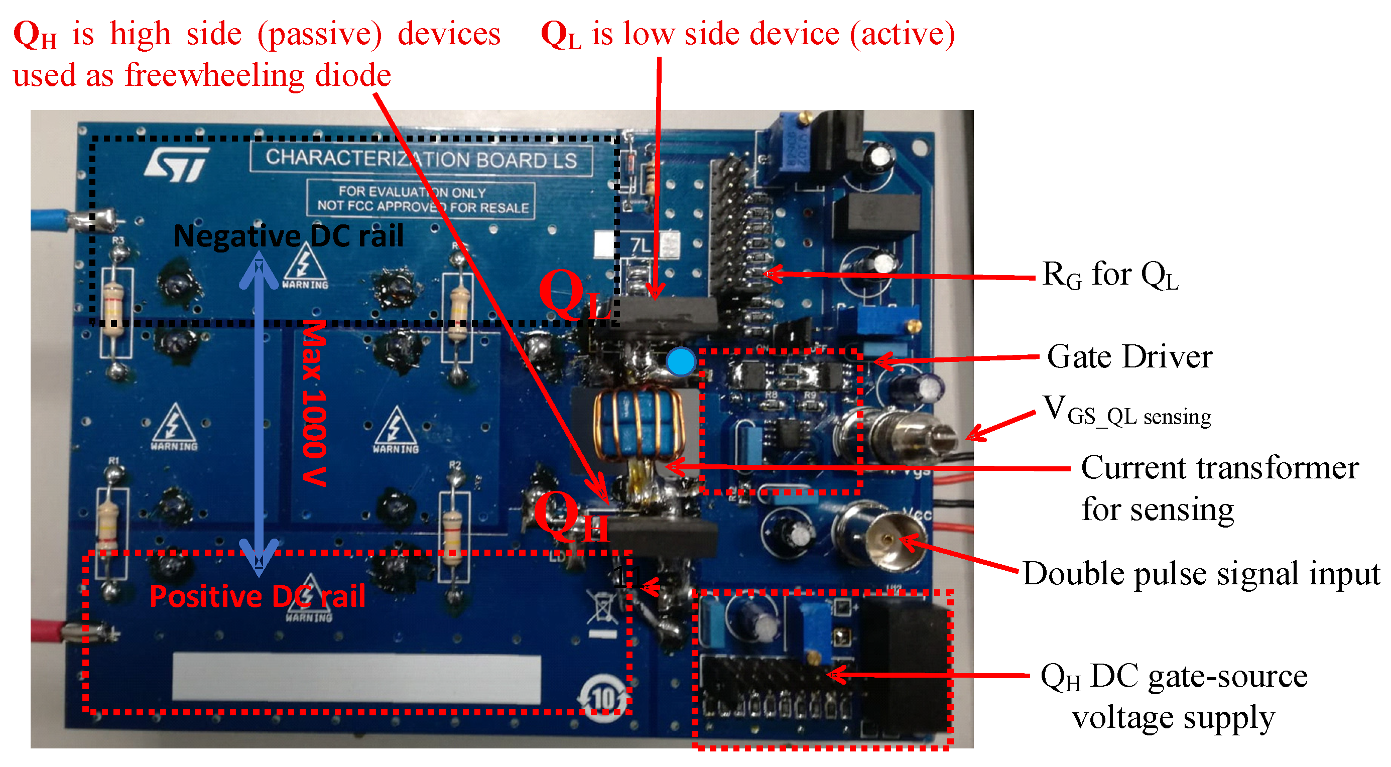
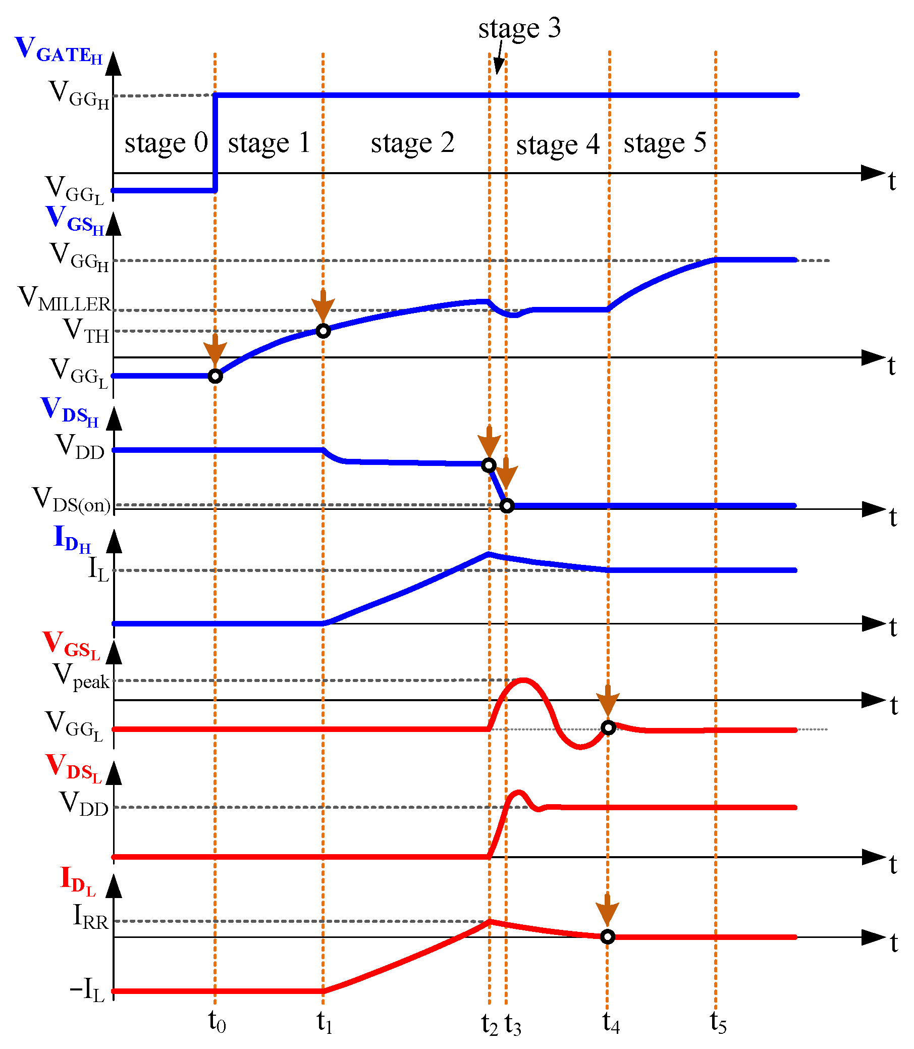
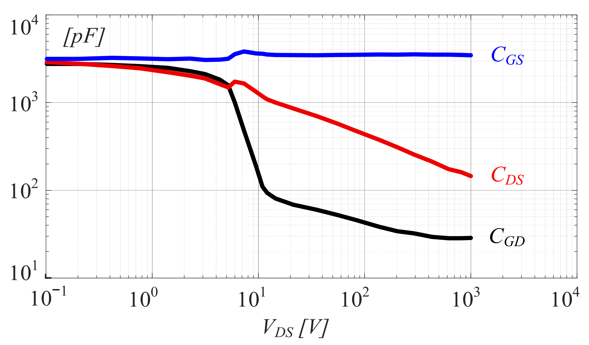
The proposed parameters identification method is applied to the SiC MOSFETs half-bridge topology shown in Figure 1, while the experimental test board is displayed in Figure 2. The half-bridge converter considered in this study includes the main parasitic elements of the PCB layout, and parasitics of each single device, such as the intrinsic capacitances and inductances related to the packaging. The parasitic inductances are extracted by monitoring the turn-on switching transients of power devices, as shown in Figure 3, whereas, the intrinsic parasitic capacitances C G S ( V D S ) , C D S ( V D S ) and C G D ( V D S ) are included in the proposed model as function of the drain-source voltage, using look-up tables, as displayed in Figure 4. In addition, the inductive contributions due to the bonding wires have been also considered as well. Moreover, an external inductive load is connected to the output converter terminals. In particular, the inductances L G B W , L D B W , and L S B W are related to the type of assembly linking the device’s die to the package (TO247-3L), while L G L E A D , L D L E A D , and L S L E A D are those related to the leads of the package. The contributions of all other parasitic external elements are resumed in the figure in three contributions named L G E X T , L D E X T , and L S E X T . The inductive load L is parallel connected to the low-side SiC MOSFET power device and can be considered a constant current source I L because of the typical large value of L . The DC power voltage source is indicated with V D D , while the control signals applied at the gate-source terminals of the high-side and low-side power devices are respectively indicated as V G A T E H and V G A T E L . Moreover, the external “kelvin-source” and thus the corresponding inductive contribution L W I R E has also been considered in the equivalent circuit. The turn-on transient of the high-side power device is carried out by dividing the entire transient into different stages, as shown in Figure 3, guaranteeing a good trade-off between the accuracy and computational burden. During the entire switching transient, the low-side SiC MOSFET is maintained in the off-state. The turn-on switching phase reported in Figure 3 is emulated by suitably rearranging the following relationships for each stage of the switching power device transient as follows:
V G S H = V D S H + V G D H
V G S L = V D S L + V G D L
I G H = C G S H V ˙ G S H + C G D H V ˙ G D H
I G L = C G S L V ˙ G S L + C G D L V ˙ G D L
I D H = C D S H V ˙ D S H C G D H V ˙ G D H + I C H H
I D L = C D S L V ˙ D S L C G D L V ˙ G D L + I C H L
V G A T E H = L G H I ˙ G H + V G S H + R G H I G H + L s B W I ˙ G H + I ˙ D H
V G A T E L = L G L I ˙ G L + V G S L + R G L I G L + L s B W I ˙ G L + I ˙ D L
V D D = L D H I ˙ D H + V D S H + L s B W I ˙ G H + L s H I ˙ D H + L D L I ˙ D L + V D S L + L s B W I ˙ G L + L s L I ˙ D L
I D H = I D L + I L
R G H = R G H E X T + R G H I N T
R G L = R G L E X T + R G L I N T
L G H = L G B W + L G H E X T + L H W I R E + L G L E A D
L D H = L D B W + L D H E X T + L D L E A D
L S H = L S B W + L S H E X T + L S L E A D
L G L = L G B W + L G L E X T + L L W I R E + L G L E A D
L D L = L D B W + L D L E X T + L D L E A D
L S L = L S B W + L S L E X T + L S L E A D
I C H H = g f s V G S H V T H H   I C H L = g f s V G S L V T H L
V G S H E X T = V G A T E H R G H E X T I G H L G H E X T + L H W I R E I ˙ G H =                                                             = V G S H + R G H I N T I G H + L G B W + L S B W + L G L E A D I ˙ G H + L S B W I ˙ D H
V D S H E X T = V D S H + L D B W + L D L E A D + L S B W I ˙ D H + L S B W I ˙ G H
V G S L E X T = V G A T E L R G L E X T I G L L G H E X T + L H W I R E I ˙ G L =                                                             = V G S L + R G L I N T I G L + L G B W + L S B W + L G L E A D I ˙ G L + L S B W I ˙ D L
V D S L E X T = V D S L + L D B W + L D L E A D + L S B W I ˙ D L + L S B W I ˙ G L
The above mathematical expressions can be solved with an iterative cycle, as described in detail in [10].

4. Problem Statement

The proposed multi-objective optimization algorithm exploits this model to identify the parasitic elements of the equivalent circuit shown in Figure 1. The unknown parasitic parameters are identified by minimizing the errors between simulation results and experimental tests obtained in the test board displayed in Figure 2. In particular, three electric quantities are considered decisive for matching the switching transients carried out by the simulations and measured during the experimental tests: The drain current I D , the gate-source voltage V G S , and the drain-source voltage V D S . I D is a function of V G S for a given V D S . Since in the switching phases the V D S can assume a fairly wide range of values, all three quantities are variable. The experimental measured voltages and current have been carried out considering a half-bridge circuit of Figure 2. A digital oscilloscope Tektronix MSO 56B (6 channels, 1 GHz) has been employed, with the following probes and their main characteristics: a passive probe TPP1000 1 GHz for the low-side gate-source voltage; an opto-isolated probe Tektronix ISOVU 1 GHz for the high-side gate-source voltage; a Lecroy HVP120 400 MHz for the low-side drain-source voltage; a THDP0200, ±1500 V 200 MHz for the high-side drain-source voltage; and a TCP0020 20Arms 50 MHz combined with a current transformer with a 10:1 ratio for the drain current. Although the parasitic effects of the probes have not been considered, noise was minimized by using probes with a high common mode rejection ratio (CMRR > 60 dB at 100 kHz) and by keeping the connection leads as short as possible. In addition, BNC adapters were used to shield the measurement setup and reduce potential ground-coupled interference.
The parasitic elements affecting the transient response are also defined in the problem for a total of 14 parameters: L G B W , L D B W , L S B W , L G L E A D , L D L E A D , L S L E A D , L G H E X T , L D H E X T , L S H E X T , L G L E X T , L D E X T , L S E X T , L H W I R E , and L L W I R E .
The problem is multi-objective and requires minimizing the cumulative differences between the transient profiles of I D t , V G S t , and V D S t of each power switch achieved by the simulations of the mathematical model with the corresponding experimental measurements. We consider the Fréchet distance as a measure of similarity between curves. The solutions to the problem will therefore be all the possible combinations of the 14 parameters (considered as real, continuous values within the range of physically feasible values), minimizing these differences, hereafter named as I D , V G S , and V D S .

5. The M9DSE Software

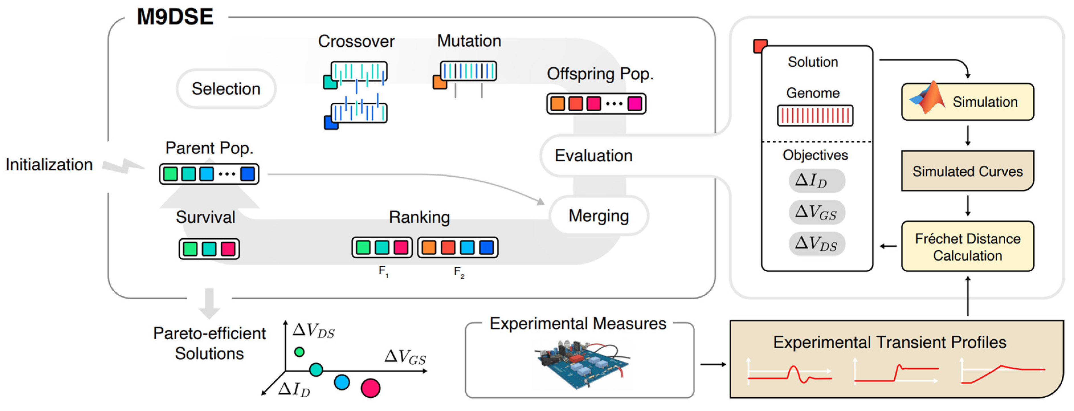
The M9DSE software implements the multi-objective genetic algorithm for the parametric exploration of the problem described in the previous section. It performs two tasks: the execution of the genetic algorithm and the validation of the results obtained at each generation by means of model simulations on MATLAB 2024b. The overall identification procedure is illustrated in the flow chart shown in Figure 5.

5.1. Inputs

To operate, M9DSE needs the following inputs:
  • A set of n values chosen by the user for each of the 14 parameters of the problem, also known as the configuration space;
  • A seed, used for random execution;
  • A size for the initial population, necessarily divisible by 2;
  • A value between 0 and 1 for the probability of crossover;
  • A value between 0 and 1 for the probability of mutation;
  • The number of generations to explore.

5.2. Genetic Process

After receiving the inputs, the genetic process begins:
(1)
Random generation of the starting population:
(a)
Generation of an individual composed of its 14 parameters with respective values randomly taken from the configuration space;
(b)
A simulation on MATLAB of the generated individual and the assignment of I D , V G S and V D S based on the comparison with experimental tests;
(c)
Repetition from (a) until the number of individuals chosen for the initial population is generated.
(2)
Application of the crossover and mutation operators to the current population based on respective probabilities.
(3)
Simulation in MATLAB of any individuals generated in the previous step, with the relative assignment of the I D , V G S , and V D S .
(4)
Selection of non-dominated individuals in the current population and elimination of any dominated individual.
(5)
Repetition starting from step (2) until the chosen number of generations is reached.

5.3. Results of the Process

The result of the process will be a set containing all the non-dominated solutions surviving up to the last generation, i.e., the optimal Pareto set, which is shown in real-time on a web interface, where the user can view each individual with all its characteristics and with a portion of MATLAB script containing the parameters of the individual selected to view the graphs relating to the latter. It is also possible to insert target values to highlight the elements that meet this objective. Finally, it is possible to save the whole Pareto set in a file, for example, TSV, to consult it in the future or to process it with data analysis algorithms. The errors I D , V G S and V D S between the simulated and measured quantities assigned to each individual can vary in a wide operating range, so the best solution will be the one that has these errors closest to zero.

6. Parametric Exploration with M9DSE

The multi-objective genetic algorithm (MOGA) has been employed for the purpose of identifying the parasitic elements of a half-bridge converter using SiC power MOSFETs. The specifications of these components can be found in Table 1. The ranges within which the parasitic parameters vary, as considered in this investigation, are detailed in Table 2. The reference experimental tests have been performed by implementing a double-pulse test (DPT) with I D = 50   A and DC bus voltage V D D = 800   V . For each parameter of the model (parasitic element), several exploration tests were carried out in which the size of the configuration space, the size of the initial population, and the number of generations to be performed were gradually increased in order to better explore the effective solution space, finding the best compromise between computational burden and simulation accuracy.

6.1. Population

In particular, it was noted that a population with few individuals (<20) leads to faster execution, but at the same time is scarcer in terms of quantity and convergence to an optimal solution. Conversely, a larger population (>40 individuals) leads to a significant increase in the execution time and to the generation of many more individuals, so it was decided to use an initial population of at least 30 individuals.

6.2. Total Generations

The total number of generations also influences the execution time and the quantity of generated individuals. Naturally, more generations will result in a higher number of individuals being produced. However, an increased number of generated individuals does not necessarily guarantee the creation of superior individuals compared to those already present. At a certain point, the algorithm will converge towards a minimum, either locally or globally.

6.3. Configuration Space

The size of the configuration space does not affect the execution time of the algorithm, but does affect the characteristics of each individual generated, since each characteristic has a certain number of possible values that it can take. Initially, the configuration space was defined with vectors of ten possible values each. In a configuration of this type, the number of possible arrangements for the 14 variables of the problem will be 1410, which makes it difficult to evaluate all the possibilities, but thanks to the modus operandi of genetic algorithms, it is possible to find the optimal Pareto set of all possibilities from which to select the most suitable solutions.

6.4. Results

All simulations were conducted using fixed values for both crossover and mutation probability, 0.8 and 0.1, respectively. Setting a low crossover probability would result in fewer combinations between individuals; conversely, an excessively high value would entail combining every pair of individuals. As for what concerns the mutation probability, a high value might render the algorithm unstable and hinder convergence; striking a balance with these values is essential. The results of each simulation were processed through algorithms written in Python 3.12 language, specially designed to return various statistics, such as the minimum values obtained for I D , V G S , and V D S ; the most balanced solutions, where the profiles achieved by simulations are as close as possible to the measured ones, without giving priority to any of the three estimation errors and the incidence of each value of the configuration space, i.e., how many times it has been chosen in the Pareto set. The first simulations were performed with the same initial configuration space and the same initial population size (30 individuals). Instead, the maximum number of generations was modified to evaluate after how many generations the algorithm begins to converge. In particular, generations have varied from a few tens up to a maximum of 3500.
After conducting numerous simulations, it has been observed that the solutions start to converge once 500 generations have been taken into account. Subsequent simulations were then carried out, maintaining a minimum of 500 generations, while adjusting the configuration space using distinct strategies: (1) by increasing the number of values for each parameter, from 10 values for each vector others are added by calculating the average between each value and the next; (2) or by reducing the number of values for each parameter by discarding those values that do not appear in the individuals of the optimal Pareto set. The two methods result in distinct Pareto fronts. With method (1), a broader range of solutions is explored that may not have been encountered otherwise. However, it is worth noting that this method does not significantly impact the execution time. On the other hand, method (2) involves eliminating values that have not appeared among non-dominated individuals, leading to a larger optimal Pareto set. This approach affects the execution time due to the generation of a greater number of non-dominated individuals, thereby necessitating more crossover and mutation operations. Furthermore, analyzing the data obtained from all the explorations, it is noted that in the simulations in which the configuration space has been expanded one or more times, the parameters of the individuals come mostly from the elements added to the initial configuration space. Therefore, the best choice to explore the entire solution space is to further increase the configuration space.

6.5. Selecting the Optimal Solutions

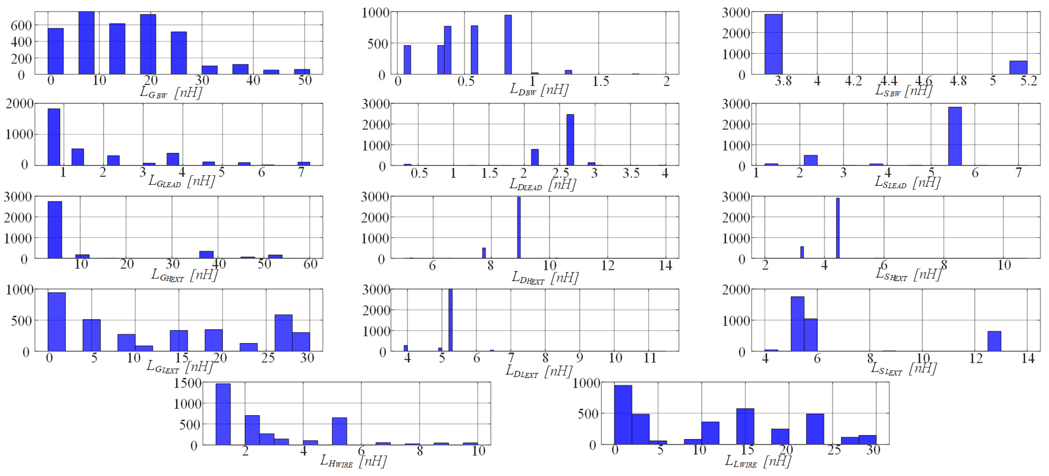
As aforementioned, each solution (set of parameters) provided by the multi-objective optimization algorithm is used in the simulations based on the analytical model given by Equations (1)–(23). The resulting profiles of I D t , V G S t , and V D S t associated with each power switch composing the half-bridge converter are compared to the experimental results. The errors I D , V G S , and V D S between the simulated and experimental results have been computed according to the multi-objective genetic algorithm described in Section 2, and a graphical representation of the corresponding Pareto surface is displayed in Figure 6. The same figure shows with red rhombuses the errors achieved by comparing the modeling using the parameters set according to a traditional approach combining FEM analysis, device’s characterization [20], and experimental tests. The distribution of the parameter values representative of the Pareto front is presented in Figure 7.
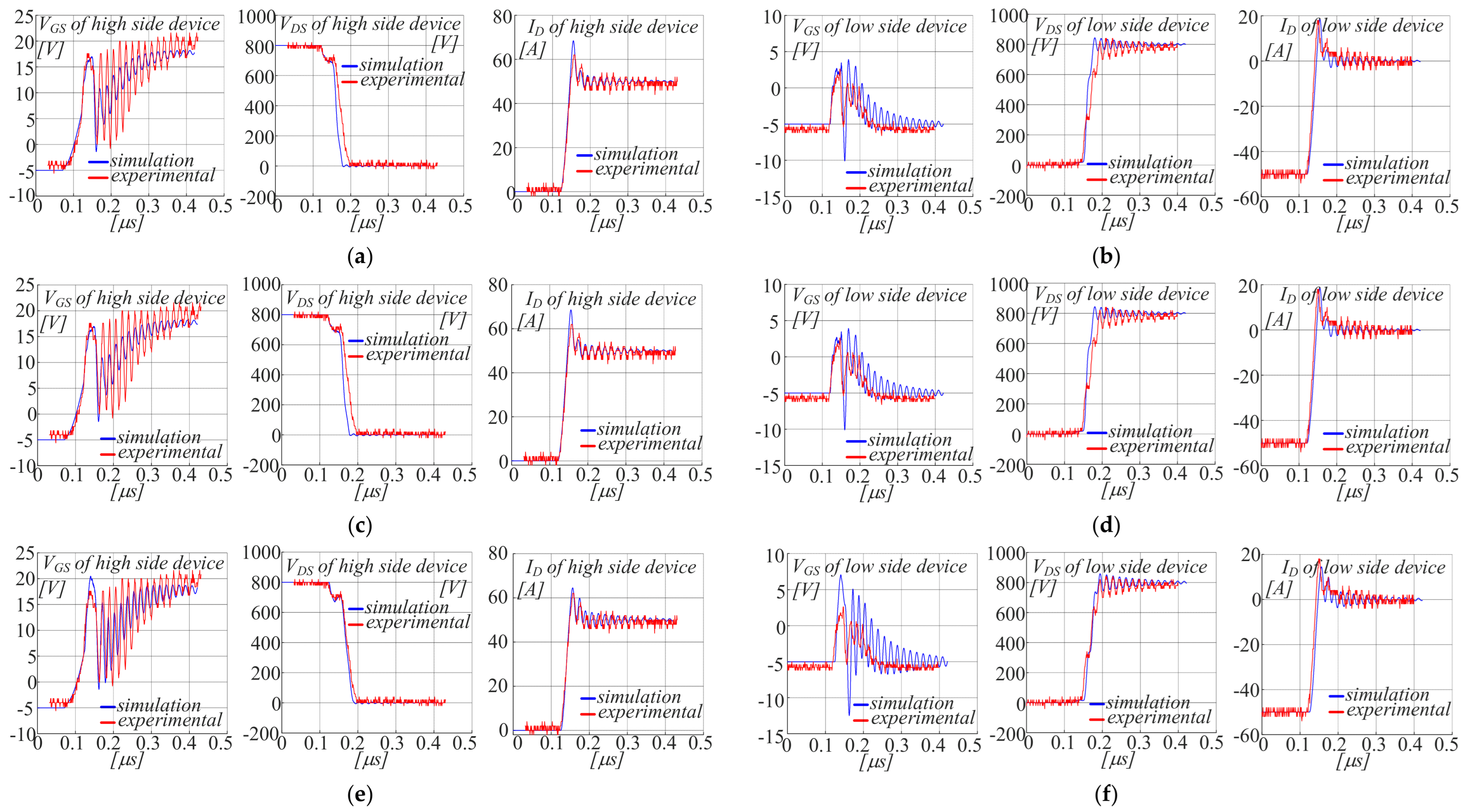
The post-processing analysis enables the observation that certain parasitic parameters predominantly exhibit a single value. Consequently, these parameters could potentially be excluded from the roster of unknown variables that the MOGA seeks to identify. Larger errors in I D , V G S , and V D S correspond to greater differences between the solutions achieved by simulations and the experimental reference measurements. The best solution would be expected to be the one minimizing all three errors, but the last condition is extremely difficult to achieve. The wide campaign of exploration carried out yielded some solutions of the Pareto front featuring satisfactory results. In particular, Figure 8 shows some representative Pareto-optimal solutions. The plots compare simulated and measured switching waveforms for solutions that minimize V G S , V D S , and I D for high-side and low-side SiC devices as detailed in the figure caption. It has been noted that when I D and V G S approach the minimum value, V D S increases considerably, usually up to 30, highlighting that the latter error conflicts with the others. The choice of the parasitic set to be integrated into the ultimate analytical model is heavily contingent on the nature of the analysis to be carried out. If the primary objective revolves around forecasting gate-source voltage stresses for the purpose of monitoring gate oxide degradation, the most suitable selection from the Pareto front would be the one that offers a more precise representation of the V G S waveform. If the primary objective of the investigation pertains to predicting stresses within the primary power loop, then a trade-off solution that balances V G S , V D S , and I D can be picked from the Pareto set.

7. Conclusions

In this work, we proposed a multi-objective optimization method to identify the principal parasitic parameters associated with the board layout and device packaging of a SiC half-bridge power converter. By minimizing the discrepancies between the simulated power converter system responses and the experimental test results, we ensure an accurate representation of real-world scenarios, demonstrated with a set of validation tests carried out on a 1200 V, 75 A, SiC half-bridge converter.
The main advantages of the proposed methodology are its accuracy, flexibility, and reduced dependency on manual tuning. The use of a multi-objective genetic algorithm (MOGA) allows the simultaneous optimization of multiple conflicting objectives, leading to a more comprehensive identification of the parasitic network. The approach also offers global optimization capability, robustness to initial conditions, and does not require gradient information, making it suitable for highly non-linear systems where analytical expressions are complex or unavailable. Furthermore, by automating the parameter identification process, the proposed method significantly reduces the overall design time and expert effort, shortening the identification procedure from several weeks of manual adjustment to only a few days of automated computation.
On the other hand, the proposed approach still requires preliminary experimental data for model validation, and its accuracy depends on the quality and representativeness of these measurements. The computational time, although much lower than that of manual or finite-element-based methods, can increase with the complexity of the circuit model and the number of objectives considered. Moreover, the current work focuses on a specific SiC half-bridge topology.
Future work will address these aspects and, in particular, will include further exploitation of the modularity and flexibility of the presented technique that, while currently validated for a specific SiC half-bridge converter topology, possesses the capability to be seamlessly adapted and extended for modeling more intricate power converter structures in the future. Overall, this study paves the way for more precise modeling of power converters, ensuring that simulated outcomes closely mirror real-world performance, thereby enhancing design reliability and efficiency.

Author Contributions

Conceptualization, L.S.; Methodology, L.D.T. and D.P.; Software, S.M.; Resources, E.R.; Data curation, M.P. (Maurizio Palesi) and M.P. (Mario Pulvirenti); Writing—original draft, S.M.; Writing—review & editing, L.D.T. and G.S.; Supervision, G.S. All authors have read and agreed to the published version of the manuscript.

Funding

This research received no external funding.

Data Availability Statement

The data presented in this study are available in this article.

Conflicts of Interest

Authors Mario Pulvirenti and Luciano Salvo were employed by the company STMicroelectronics. The remaining authors declare that the research was conducted in the absence of any commercial or financial relationships that could be construed as a potential conflict of interest.

References

  1. She, X.; Huang, A.Q.; Lucia, O.; Ozpineci, B. Review of silicon carbide power devices and their applications. IEEE Trans. Ind. Electron. 2017, 64, 8193–8205. [Google Scholar] [CrossRef]
  2. Deboy, G. Shaping the transition from Si-based power devices to SiC MOSFETs and GaN HEMTs. In Proceedings of the 2022 24th European Conference on Power Electronics and Applications (EPE’22 ECCE Europe), Hannover, Germany, 5–9 September 2022; pp. 1–2. [Google Scholar]
  3. Zhang, L.; Yuan, X.; Wu, X.; Shi, C.; Zhang, J.; Zhang, Y. Performance Evaluation of High-Power SiC MOSFET Modules in Comparison to Si IGBT Modules. IEEE Trans. Power Electron. 2019, 34, 1181–1196. [Google Scholar] [CrossRef]
  4. Chen, H.-J.; Kusic, G.L.; Reed, G.F. Comparative PSCAD and Matlab/Simulink simulation models of power losses for SiC MOSFET and Si IGBT devices. In Proceedings of the 2012 IEEE Power and Energy Conference at Illinois, Champaign, IL, USA, 24–25 February 2012; pp. 1–5. [Google Scholar] [CrossRef]
  5. Alves, L.F.S.; Lefranc, P.; Jeannin, P.-O.; Sarrazin, B. Review on SiC-MOSFET devices and associated gate drivers. In Proceedings of the 2018 IEEE International Conference on Industrial Technology (ICIT), Lyon, France, 19–22 February 2018; pp. 824–829. [Google Scholar] [CrossRef]
  6. Risseh, A.E.; Nee, H.-P.; Kostov, K. Electrical performance of directly attached SiC power MOSFET bare dies in a half-bridge configuration. In Proceedings of the 2017 IEEE 3rd International Future Energy Electronics Conference and ECCE Asia (IFEEC 2017—ECCE Asia), Kaohsiung, Taiwan, 3–7 June 2017; pp. 417–421. [Google Scholar] [CrossRef]
  7. Wu, L.; Xiao, L.; Zhao, J.; Chen, G. Physical analysis and modeling of the nonlinear Miller capacitance for SiC MOSFET. In Proceedings of the IECON 2017—43rd Annual Conference of the IEEE Industrial Electronics Society, Beijing, China, 29 October–1 November 2017; pp. 1411–1416. [Google Scholar] [CrossRef]
  8. Sadik, D.-P.; Kostov, K.; Colmenares, J.; Giezendanner, F.; Ranstad, P.; Nee, H.-P. Analysis of Parasitic Elements of SiC Power Modules with Special Emphasis on Reliability Issues. IEEE J. Emerg. Sel. Top. Power Electron. 2016, 4, 988–995. [Google Scholar] [CrossRef]
  9. DiMarino, C.M.; Mouawad, B.; Johnson, C.M.; Boroyevich, D.; Burgos, R. 10-kV SiC MOSFET power module with reduced common-mode noise and electric field. IEEE Trans. Power Electron. 2020, 35, 6050–6060. [Google Scholar] [CrossRef]
  10. Pulvirenti, M.; Montoro, G.; Nania, M.; Scollo, R.; Scelba, G.; Cacciato, M.; Scarcella, G.; Salvo, L. Analysis of transient gate–source overvoltages in silicon carbide MOSFET power devices. In Proceedings of the 2018 IEEE Energy Conversion Congress and Exposition (ECCE), Portland, OR, USA, 23–27 September 2018; pp. 1895–1902. [Google Scholar] [CrossRef]
  11. Liu, T.; Wong, T.T.Y.; Shen, Z.J. A New Characterization Technique for Extracting Parasitic Inductances of SiC Power MOSFETs in Discrete and Module Packages Based on Two-Port S-Parameters Measurement. IEEE Trans. Power Electron. 2018, 33, 9819–9833. [Google Scholar] [CrossRef]
  12. Noppakunkajorn, J.; Han, D.; Sarlioglu, B. Analysis of High-Speed PCB with SiC Devices by Investigating Turn-Off Overvoltage and Interconnection Inductance Influence. IEEE Trans. Transp. Electrif. 2015, 1, 118–125. [Google Scholar] [CrossRef]
  13. Yang, F.; Wang, Z.; Liang, Z.; Wang, F. Electrical Performance Advancement in SiC Power Module Package Design with Kelvin Drain Connection and Low Parasitic Inductance. IEEE J. Emerg. Sel. Top. Power Electron. 2019, 7, 84–98. [Google Scholar] [CrossRef]
  14. Wang, L.; Zhang, T.; Yang, F.; Ma, D.; Zhao, C.; Pei, Y.; Gan, Y. Cu Clip-Bonding Method with Optimized Source Inductance for Current Balancing in Multichip SiC MOSFET Power Module. IEEE Trans. Power Electron. 2022, 37, 7952–7964. [Google Scholar] [CrossRef]
  15. Guacci, M.; Bortis, D.; Kovačević-Badstübner, I.F.; Grossner, U.; Kolar, J.W. Analysis and design of a 1200 V All-SiC planar interconnection power module for next generation more electrical aircraft power electronic building blocks. CPSS Trans. Power Electron. Appl. 2017, 2, 320–330. [Google Scholar] [CrossRef]
  16. Jørgensen, A.B.; Munk-Nielsen, S.; Uhrenfeldt, C. Overview of Digital Design and Finite-Element Analysis in Modern Power Electronic Packaging. IEEE Trans. Power Electron. 2020, 35, 10892–10905. [Google Scholar] [CrossRef]
  17. DeBoi, B.T.; Lemmon, A.N.; McPherson, B.; Passmore, B. Improved Methodology for Parasitic Analysis of High-Performance Silicon Carbide Power Modules. IEEE Trans. Power Electron. 2022, 37, 12415–12425. [Google Scholar] [CrossRef]
  18. Sellers, A.J.; Hontz, M.R.; Khanna, R.; Lemmon, A.N.; DeBoi, B.T.; Shahabi, A. An Automated Model Tuning Procedure for Optimizing Prediction of Transient and Dispersive Behavior in Wide Bandgap Semiconductor FETs. IEEE Trans. Power Electron. 2020, 35, 12252–12263. [Google Scholar] [CrossRef]
  19. Chen, J.; Peng, H.; Cheng, Z.; Liu, X.; Xin, Q.; Kang, Y.; Wu, J.; Chu, X. A Novel Power Loop Parasitic Extraction Approach for Paralleled Discrete SiC MOSFETs on Multilayer PCB. IEEE J. Emerg. Sel. Top. Power Electron. 2021, 9, 6370–6384. [Google Scholar] [CrossRef]
  20. Pulvirenti, M.; Salvo, L.; Sciacca, A.G.; Scelba, G.; Cacciato, M. Modeling of SiC-MOSFET Converter Leg Including Parasitics of 518 Printed Circuit Board Layout and Device Packaging. In Proceedings of the 2020 22nd European Conference on Power Electronics and Applications 519 (EPE’20 ECCE Europe), Lyon, France, 7–11 September 2020; pp. 1–10. [Google Scholar] [CrossRef]
  21. Umetani, K.; Aikawa, K.; Hiraki, E. Straightforward Measurement Method of Common Source Inductance for Fast Switching Semiconductor Devices Mounted on Board. IEEE Trans. Ind. Electron. 2017, 64, 8258–8267. [Google Scholar] [CrossRef]
  22. Mukunoki, Y.; Horiguchi, T.; Nakayama, Y.; Nishizawa, A.; Nakamura, Y.; Konno, K.; Kuzumoto, M.; Akagi, H. Modeling of a silicon-carbide MOSFET with focus on internal stray capacitances and inductances, and its verification. In Proceedings of the 2017 IEEE Applied Power Electronics Conference and Exposition (APEC), Tampa, FL, USA, 26–30 March 2017; pp. 2671–2677. [Google Scholar] [CrossRef]
  23. Tornello, L.D.; Spitaleri, M.G.; Scarcella, G.; Cacciato, M. Analytical modeling of SiC-MOSFETs for parasitic parameter adjustment based on experimental data. Electr. Eng. 2025, 107, 15205–15215. [Google Scholar] [CrossRef]
  24. De Leon-Aldaco, S.E.; Calleja, H.; Aguayo Alquicira, J. Metaheuristic Optimization Methods Applied to Power Converters: A Review. IEEE Trans. Power Electron. 2015, 30, 6791–6803. [Google Scholar] [CrossRef]
  25. Wu, X.; Yang, X.; Ye, J.; Liu, G. Novel Prognostics for IGBTs Using Wire-Bond Contact Degradation Model Considering On-Chip Temperature Distribution. IEEE Trans. Power Electron. 2025, 40, 4411–4424. [Google Scholar] [CrossRef]
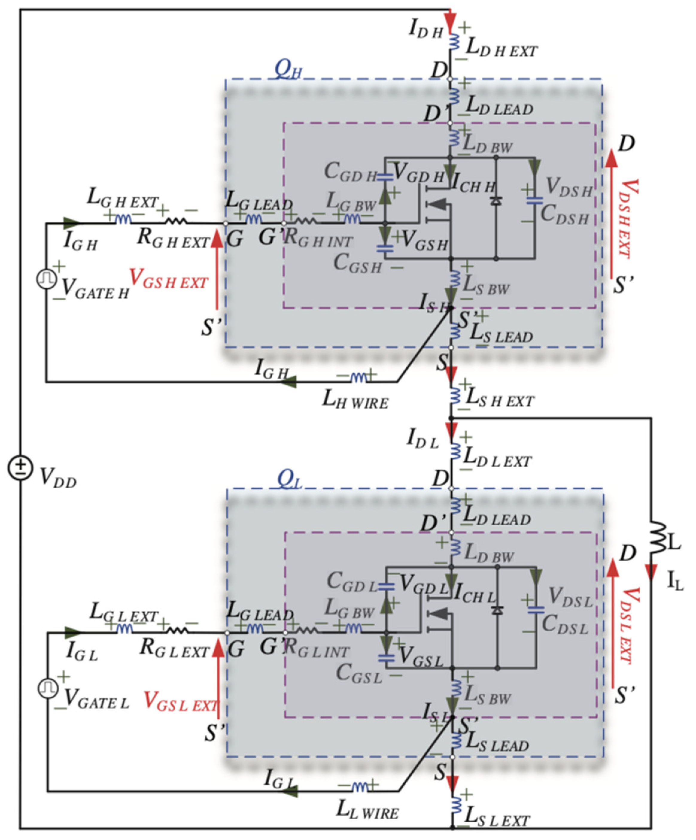
Figure 1. Equivalent circuit of the half-bridge configuration including parasitic elements.
Electronics 14 04458 g001
Figure 2. Experimental test board.
Electronics 14 04458 g002
Figure 3. Turn-on switching phases of the high-side SiC MOSFET, [20].
Electronics 14 04458 g003
Figure 4. SiC MOSFET intrinsic parasitic capacitances variation with drain-source voltage.
Electronics 14 04458 g004
Figure 5. Flow chart of the identification procedure with the M9DSE algorithm.
Electronics 14 04458 g005
Figure 6. Individual 2D representations of the Pareto front: black rhombus (minimized V G S ), red rhombus (minimized V D S ) and green rhombus (minimized I D ).
Electronics 14 04458 g006
Figure 7. Parameter values distribution in the Pareto front.
Electronics 14 04458 g007
Figure 8. Simulation of the Pareto solution vs. respective measured values: (a) to minimize V G S for high-side SiC devices and (b) for low-side SiC devices; (c) to minimize I D for high-side SiC devices and (d) for low-side SiC devices; and (e) to minimize V D S for high-side SiC devices and (f) for low-side SiC devices.
Electronics 14 04458 g008
Table 1. SCTW70N120G2V SiC MOSFET specifications.
ParameterValue
V D S 1200 V
R D S ( o n ) @ V G S = 18   V , I D = 50   A , T = 25   ° C 21 mΩ
V G S (Maximum Operative Range)−10 V/+22 V
V T H @ I D = 1   m A , T = 25   ° C 2.45 V
Table 2. Range, default value (i.e., first investigated value), and value that leads to the minimum V G S , of the model’s parameters.
ParameterRangeDefault Value Value   for   Min   V G S
L G I N T 1–50 nH2 nH1 nH
L D I N T 0.1–2 nH0.38 nH0.575 nH
L S I N T 1–12 nH3 nH3.75 nH
L G P I N 0.7–7 nH3 nH0.7 nH
L D P I N 0.4–4 nH3 nH2.65 nH
L S P I N 0.7–7 nH3 nH5.425 nH
L G H E X T 4–60 nH6 nH4 nH
L D H E X T 4–14 nH5 nH9 nH
L S H E X T 2–12 nH6 nH3.25 nH
L G L E X T 1–30 nH6 nH4.625 nH
L D L E X T 4–14 nH5 nH5.25 nH
L S L E X T 4–14 nH6 nH5.25 nH
L H W I R E 1–10 nH2.5 nH1 nH
L L W I R E 1–30 nH2.5 nH15.5 nH
Disclaimer/Publisher’s Note: The statements, opinions and data contained in all publications are solely those of the individual author(s) and contributor(s) and not of MDPI and/or the editor(s). MDPI and/or the editor(s) disclaim responsibility for any injury to people or property resulting from any ideas, methods, instructions or products referred to in the content.