1. Introduction
Radiation-hardened integrated circuits are a necessity for applications in space, high-energy physics, and nuclear facilities where ionizing radiation causes total dose (TID) degradation of the integrated devices as well as reversible and irreversible single-event effects (SEEs) from high-energy particles. Early systems relied heavily on radiation-hardened by shielding (RHBS) techniques, using dense materials to block external radiation. However, as modern systems demand extreme miniaturization and low-mass designs, RHBS has become less favorable. Moreover, shielding materials can provide only a certain level of protection against high-energy radiation; for example, heavy ions may penetrate shields more effectively than lighter particles, rendering the components still vulnerable to radiation-induced failures [
1]. Over the past two decades, specialized semiconductor processes have been developed to achieve radiation hardening by process (RHBP). However, RHBP introduces challenges, including significantly higher fabrication costs [
2], increased power [
3] and area overhead [
4], and greater manufacturing complexity [
5]. Despite offering improved radiation tolerance, RHBP may still leave systems vulnerable under certain exposure scenarios, making it essential to weigh cost, performance, and reliability trade-offs when selecting hardening strategies [
2,
3,
4,
5]. Furthermore, modern deep submicron CMOS technologies, with their thinner gate oxides, exhibit greater intrinsic tolerance to TID effects because of reduced threshold voltage shifts, making commercial processes increasingly attractive [
6]. However, despite the high tolerance of the gate oxide, radiation-induced edge effects such as charge trapping in isolation structures can still lead to leakage currents and other degradation mechanisms in deep submicron processes [
7]. This has shifted the research focus toward radiation hardening by design (RHBD), which enables the use of standard CMOS while improving radiation resilience through circuit and architecture-level techniques [
8]. RHBD offers significant benefits, including reduced cost, better power efficiency, and design flexibility. Techniques such as Triple Modular Redundancy (TMR), Error Detection and Correction (EDAC), and selective node hardening allow designers to target only critical components, minimizing area and energy overhead [
9,
10]. As a result, RHBD has become the preferred strategy in modern radiation-tolerant design due to its balance of reliability, efficiency, and scalability.
Analog-to-digital converters (ADCs) are essential mixed-signal components in radiation-sensitive systems because they serve as front-end interfaces for sensor data acquisition and signal processing. Due to their inherent mixed analog-digital structure, ADCs are particularly susceptible to SEE-induced bit flips and TID-related parameter drifts, leading to degradation in conversion accuracy and circuit stability. Surveys of ADC behavior under ionizing radiation confirm these vulnerabilities across both commercial and hardened architectures [
11,
12]. Therefore, the development of robust radiation-hardened ADC architecture has emerged as a central focus within high-reliability sectors, notably in aerospace and nuclear applications [
13].
This work presents the design and simulation of a radiation-hardened 4-bit flash ADC implemented in a 22 nm FD-SOI process. The flash architecture was selected for its simplicity, which allows radiation-induced errors to be more clearly isolated from the converter’s intrinsic inaccuracies, enabling a focused evaluation of radiation effects on mixed-signal circuits. The design incorporates multiple hardening strategies, including dual modular redundancy (DMR)–based error detection and correction logic, sequential comparator activation to reduce power, and the use of thin-oxide devices in analog-critical paths to improve total ionizing dose (TID) tolerance. The measures presented in this work are independent of ADC architecture and, combined with the inherent advantages of SOI technology, result in a scalable and efficient solution for reliable data acquisition in radiation-intensive environments.
The remainder of this paper is organized as follows.
Section 2 introduces the proposed radiation-hardened ADC architecture.
Section 3 discusses the circuit-level hardening techniques and the single-event transient (SET) pulse modeling framework used for radiation effect evaluation.
Section 4 presents the post-layout simulation results, covering functional verification, radiation pulse injection analysis, and power consumption. Finally,
Section 5 concludes the paper.
2. Radiation Hardened by Design (RHBD) ADC
Typically, Radiation Hardening by Design (RHBD) uses techniques at the architecture, circuit, and layout levels. Enclosed layout transistors (ELTs) are often effective for improving radiation tolerance [
8]. However, this work uses a 22 nm Fully Depleted Silicon-On-Insulator (FD-SOI) process whose design rules prohibit ELTs, which limit layout-level hardening. In FD-SOI, devices are isolated by the buried oxide (BOX), which removes the parasitic p-n-p-n path formed by adjacent PNP/NPN parasitic BJTs in bulk CMOS. As a result, classical single-event latch-up (SEL) is inherently suppressed in this technology. Therefore, our focus in this design is primarily directed towards strengthening the architecture and circuit-level strategies.
ADCs can be implemented in several architectures, such as SAR, pipeline, sigma-delta, and flash, each offering trade-offs in resolution, sampling rate, and radiation tolerance [
12,
13,
14,
15]. SAR ADCs are widely used for their balanced resolution and power efficiency, with lower power dissipation and smaller die areas compared to flash ADCs at higher resolutions [
13]. However, their sequential operation introduces vulnerability to SEEs, particularly in flip-flops and capacitor arrays [
16]. Although hardened designs exist, they usually involve extra circuitry that increases complexity and area [
16]. Pipeline ADCs provide high throughput and resolution by dividing the conversion process into multiple stages [
12,
17]. However, each stage relies on precise analog components like amplifiers and comparators, which are sensitive to radiation-induced faults. Errors in early stages can propagate through the pipeline, degrading output accuracy and making error correction more difficult [
12,
18]. Delta-sigma ADCs achieve high resolution and excellent noise performance in low-frequency applications through oversampling and noise shaping [
19]. However, delta-sigma converters typically operate at lower speeds, which can hinder their effectiveness in high-rate applications found in radiation environments [
15,
19]. Moreover, their complex feedback architecture can introduce additional susceptibility to radiation-induced errors [
19]. Flash ADCs provide the highest sampling rates, using a parallel comparator architecture for fast conversion [
14]. While resolution is limited to 4–6 bits, they have been widely used in the past due to their simplicity, low latency, and suitability for high-speed, low-bit applications [
13,
14]. The straightforward structure also allows for easier integration of fault-tolerant techniques, making them more robust against SEE-induced bit flips [
13,
20].
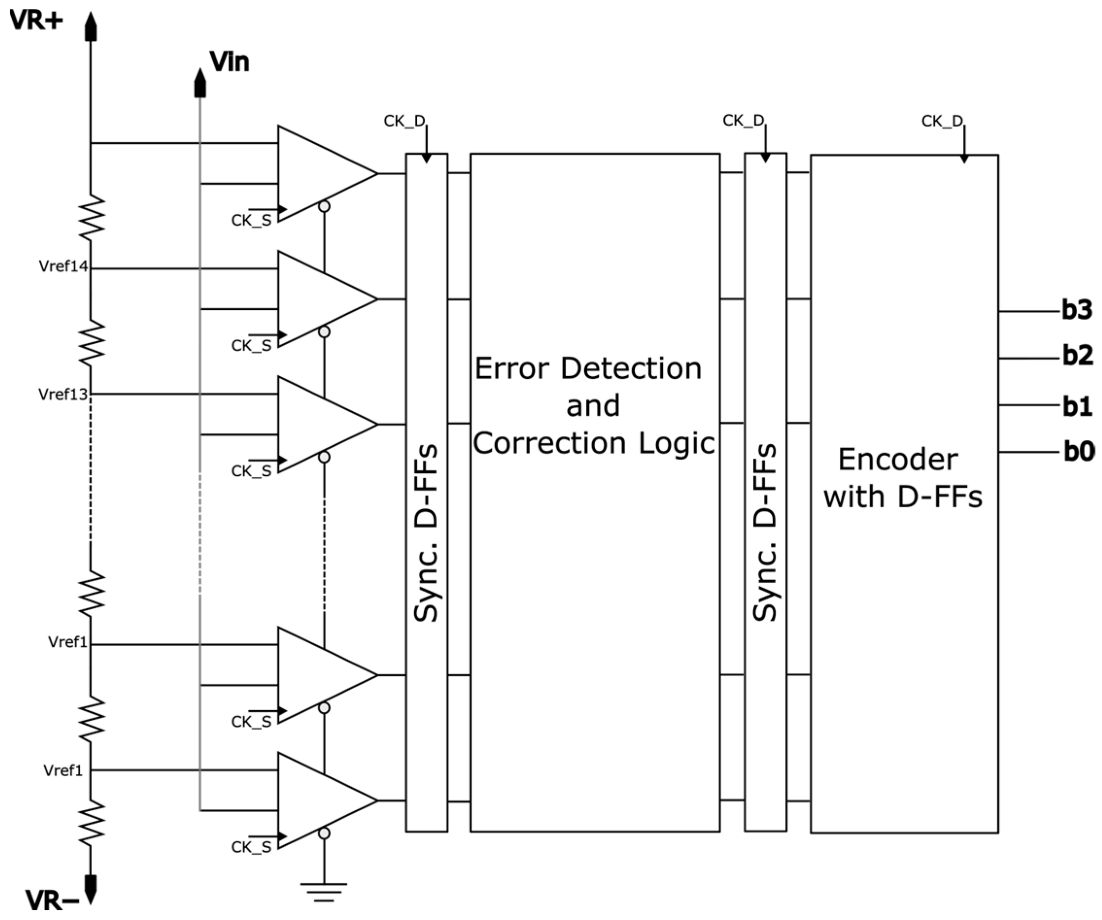
The proposed 4-bit flash ADC, shown in
Figure 1, consists of a resistive reference ladder generating comparison voltages, followed by 2
n distributed sample-and-hold (S/H) stages integrated with comparators. This distributed sampling adds redundancy to the input path, improving robustness against single-event upsets. A synchronizing Digital Flip-Flop (DFF) stage follows the comparator array to stabilize outputs before further processing. Error detection and correction logic is then applied, enabling recovery from SEU-induced bit flips while avoiding the full overhead of triple modular redundancy. A second synchronizing DFF stage ensures stable transfer of corrected thermometer-code data into the binary encoder. Finally, the thermometer-to-binary encoder produces the 4-bit digital output, which is latched again by an output DFF stage to guarantee reliable timing closure.
3. Circuit Level Design
In this work, each circuit block was designed with specific radiation-hardening considerations, based on its sensitivity to radiation-induced effects. For the analog front-end, Total Ionizing Dose (TID) effects were a primary concern. Ionizing radiation generates electron–hole pairs in the oxide, where holes can become trapped, leading to charge buildup that induces threshold voltage (Vth) shifts, parasitic leakage currents, and degradation of transconductance (gm) in MOS devices.
It is well established that devices with thicker gate oxides are more susceptible to threshold voltage shifts due to oxide-trapped charge and interface-trap charge accumulation [
21]. The total threshold voltage shift can be expressed as:
where each contribution is determined by
Here, Cox is the gate oxide capacitance per unit area, tox is the oxide thickness, and (ot,it)(x) represents the spatial distribution of radiation-induced oxide-trapped charge/interface-trap charge density within the oxide.
To mitigate TID effects, thinner oxides are preferred. A thinner tox increases the probability of electron–hole recombination and enhances tunneling of electrons through the oxide, thereby reducing net trapped charge. This physical mechanism minimizes threshold voltage degradation under prolonged radiation exposure.
The 22 nm Fully Depleted Silicon-On-Insulator (FD-SOI) process employed in this work offers two gate oxide options: thin-oxide transistors with
tox ≈ 1.25 nm and medium-oxide transistors with
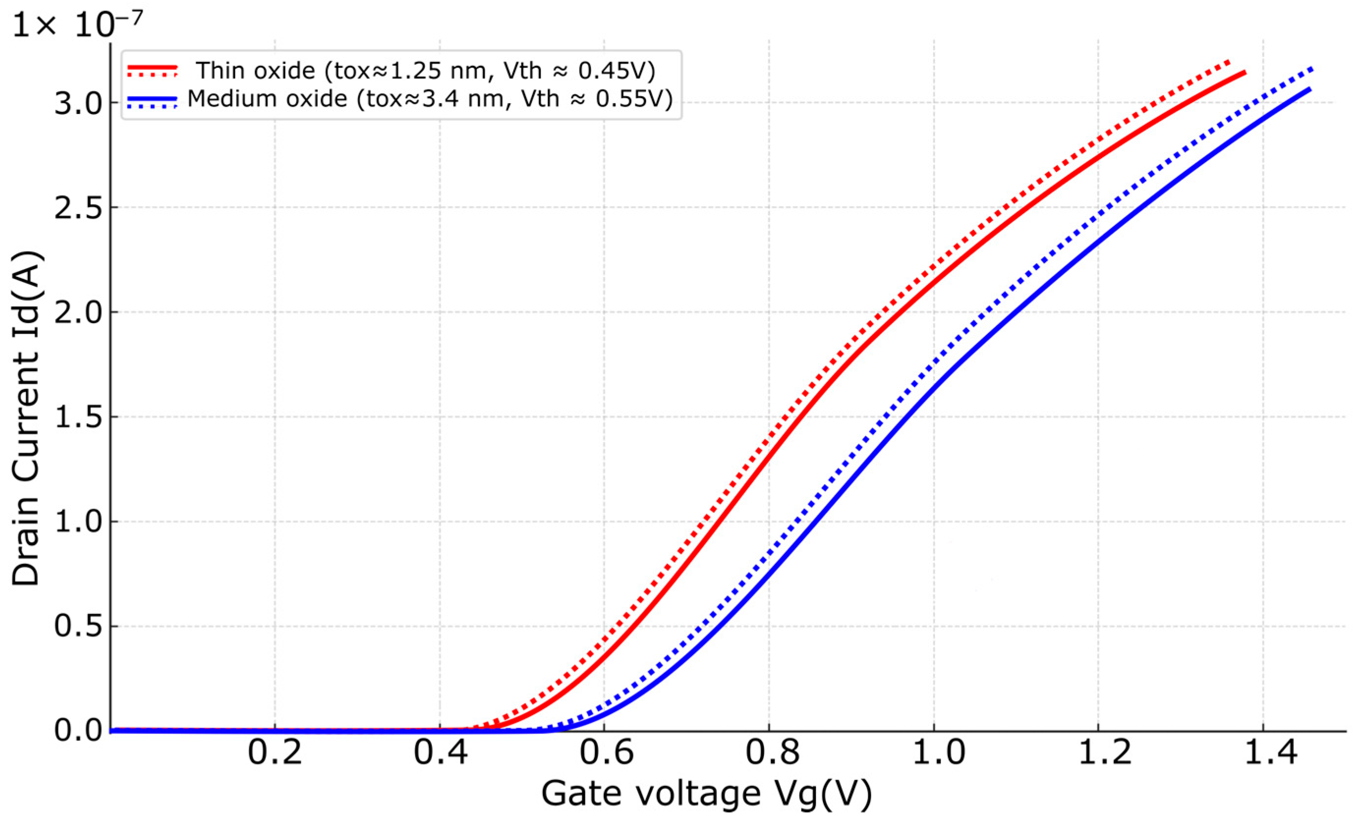
tox ≈ 3.4 nm. To evaluate their TID response, NMOS devices with both oxide configurations were modeled in Synopsys Sentaurus TCAD. Device structures were constructed in Sentaurus Structure Editor (SDE), and simulations were performed under a cumulative dose of 1 Mrad (Si). Post-irradiation
ID–
VG characteristics were analyzed to extract threshold voltage shifts.
Figure 2 shows the simulated radiation generation profile across the SOI device, while
Figure 3 presents the simulated
ID–
VG characteristics for thin-oxide and medium-oxide NMOS devices before and after irradiation.
The results indicate that the thin-oxide device exhibited only ~1.5% threshold voltage shift (~4 mV), while the medium-oxide device showed a larger shift of ~5.5% (~15 mV). Although these shifts appear small, even modest threshold variations can significantly affect bias stability, gain, and linearity in analog circuits. Based on these results, thin-oxide devices were adopted throughout all analog-critical paths in the ADC to enhance tolerance against TID effects.
3.1. Sample-and-Hold Circuit
The sample-and-hold (S/H) stage forms the front end of the ADC and is responsible for capturing the input voltage prior to quantization. In radiation-sensitive environments, the design of this block must account for both total ionizing dose (TID) degradation and Single-Event Effects (SEEs). In our implementation, a distributed S/H architecture is adopted, where each comparator is paired with its own local sampling capacitor and latch. This scheme enhances SEE tolerance by localizing the impact of a heavy ion to the affected sampling node, which can be recovered in the subsequent error correction stage. In addition, a sequential comparator activation scheme is introduced to reduce both power consumption and radiation vulnerability.
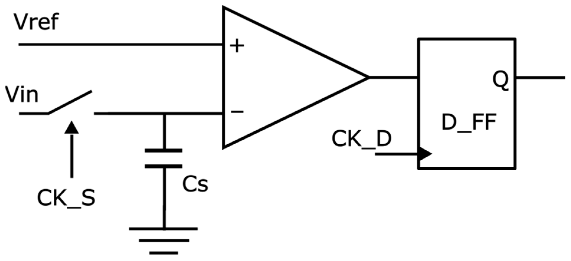
As illustrated in
Figure 4, the S/H circuit consists of complementary transmission gates controlled by a sampling clock (CK_S) that connects the analog input (Vin±) to the sampling capacitor (C
s). During the sampling phase, when CK_S is high, the switches conduct, allowing the capacitors to track the input voltage. As CK_S transitions low, the switches turn off, isolating the capacitors and preserving the sampled value for comparison. Parasitic charge injection and clock feedthrough are mitigated through careful switch sizing, the use of non-overlapping clocks, and symmetric layout practices.
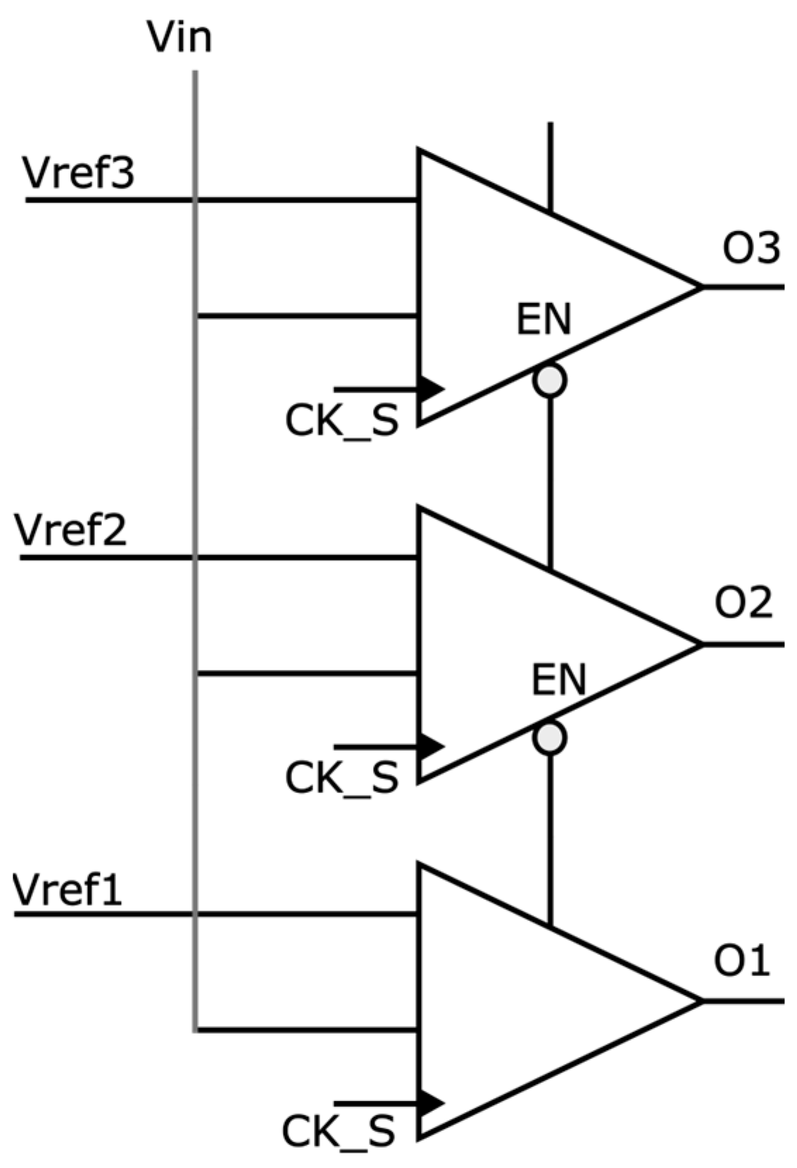
Unlike conventional flash ADCs, which enable all comparators simultaneously, the proposed architecture dynamically activates only the required comparators, reducing both power and SEE exposure. Comparators are arranged in a chained configuration, starting from the lowest reference voltage as illustrated in
Figure 5. The lowest comparator is always active. When CK_S is asserted, all comparators latch their local S/H input, but only the lowest comparator evaluates its input initially. If the comparator output indicates that the input exceeds its reference, it enables the next comparator in the chain. This process continues until the first comparator detects that the input is below its reference level, at which point no further comparators are activated.
This sequential activation ensures that only the minimum number of comparators are powered on during each conversion. For a 4-bit ADC with 15 comparators, and assuming a uniform input distribution, the average number of active comparators is approximately half of the total:
Thus, the scheme provides an approximately 50% reduction in dynamic power compared to full parallel activation. This not only improves energy efficiency but also reduces the number of nodes exposed to SEUs at any given time. Comparators turn on in a natural order as the enable fans out across the array, and small local delays create a small, fixed spread. Because it comes from the same clock, it is repeatable, not random jitter. In post-layout simulations at 20 MHz, the spread stayed a small fraction of the 50 ns period, all comparators settled before the digital latch samples their outputs, and throughput was unchanged. We enable comparators after the sample is held and keep a short guard time, which prevents metastability.
Sampling Capacitor Selection for SEE Tolerance
The sampling capacitor at the comparator input directly affects how much voltage disturbance a high-energy particle strike can cause. This is particularly critical at the first comparator stage, where the input signal is smallest and the node is most vulnerable. A charged particle depositing sufficient energy at this point can shift the sampled voltage enough to flip the comparator decision.
To quantify this, the critical charge is expressed as
Here, CS is the sampling capacitor and Vmargin is the minimum voltage swing that could alter the comparator’s decision. Increasing CS raises the required collected charge for an upset, thereby improving SEE tolerance. However, larger capacitance also increases sampling time and dynamic power, introducing a trade-off between robustness and speed.
In this work, a capacitor value of 250 fF was selected. This choice was validated using the single-event transient (SET) current source model described in
Section 3.4, ensuring that the capacitor provides sufficient immunity against expected charge deposition levels while maintaining adequate speed for 4-bit flash ADC operation.
3.2. Error Detection and Correction for Thermometer Code
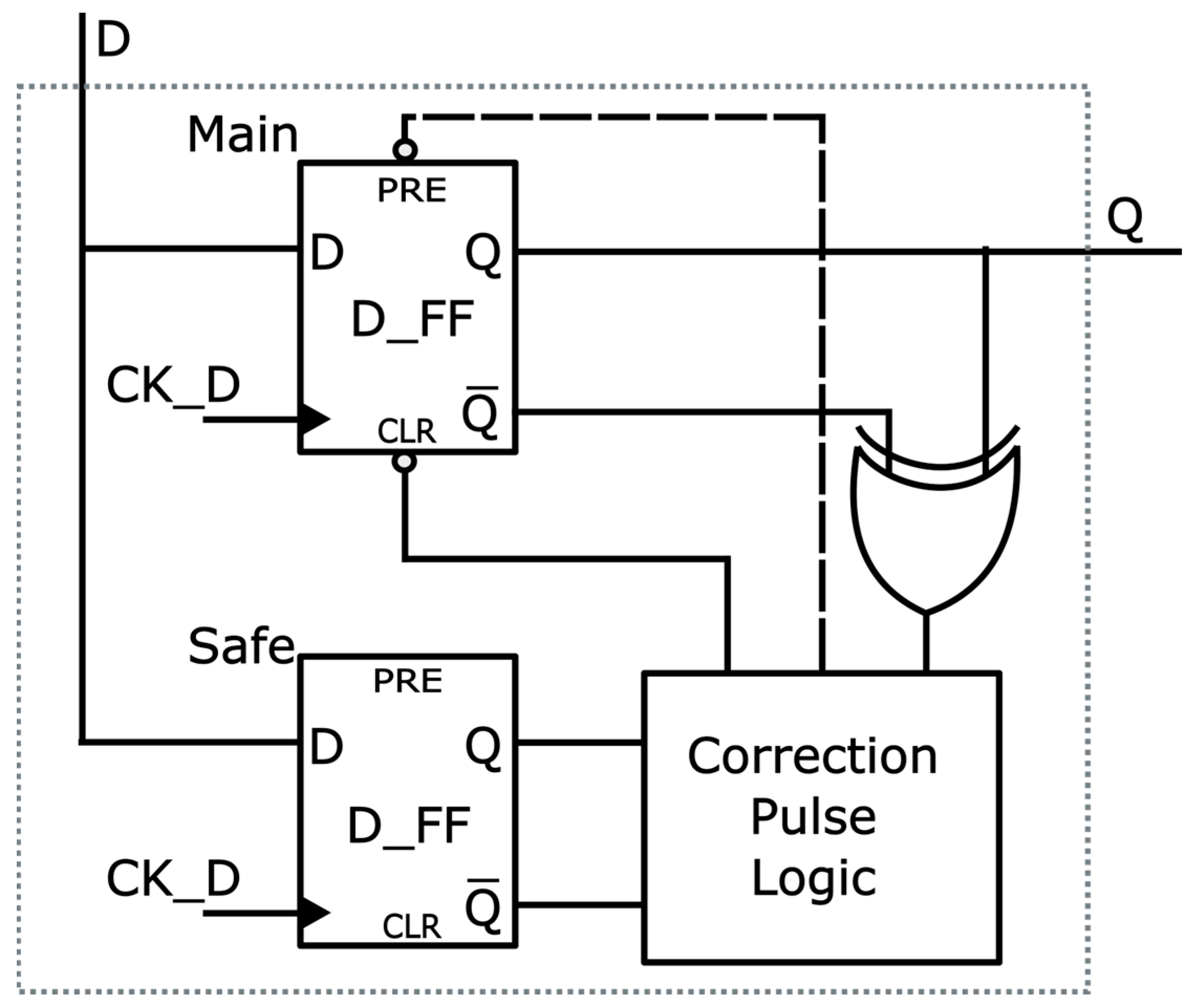
To improve the reliability of the thermometer code generated by the comparator array, a custom error detection and correction scheme is implemented to recover from Single Event Upsets (SEUs). The error correction scheme is illustrated in
Figure 6. Each thermometer bit is stored in two D_FFs: one holds the primary data, and the other maintains a safe backup copy.
An XOR gate continuously monitors the primary D_FF by comparing its and outputs. Under normal conditions, and remain complementary. If an SEU momentarily disturbs the D_FF, causing and to become equal, the XOR gate flags the event and generates a correction pulse. This pulse reloads the corrupted D_FF from its backup copy, restoring the correct thermometer code value without requiring pipeline reset.
If an upset occurs only in the backup D_FF, the fault remains undetected but does not affect the digital output. In the rare case where both DFFs are upset simultaneously, recovery is not possible, similar to TMR when two of the three nodes are corrupted [
22]. Nevertheless, the proposed scheme achieves error-correction comparable to TMR while using only two storage nodes instead of three, which reduces storage elements by 33%. It also replaces the majority voter with a simple XOR-based check, and majority voters are reported to incur higher area, power, and switching activity than simple gate networks in 32/28 nm CMOS [
10], while TMR inherently carries the triplication overhead [
22].
3.3. Digital Logic Design
The digital logic used for thermometer-to-binary encoding, error correction, and control in this work is designed with an emphasis on improving tolerance to Single Event Transients (SETs). Rather than employing full redundancy, the design applies circuit-level hardening rules that improve robustness with minimal overhead in area and power.
A primary strategy is to minimize transistors that lack a defined connection to either V
DD or V
SS. Floating or weakly driven nodes are more susceptible to radiation-induced charge deposition, which can alter logic states with relatively small transients [
23]. By ensuring that most transistors have at least one terminal tied to a stable reference (either V
DD or ground), any injected charge must generate a voltage swing large enough to cross the threshold before it can toggle a gate. This increases the critical charge required for an upset, effectively filtering out low-level transients and reducing soft error rates in combinational logic.
This design practice is followed throughout the digital backend. Logic gates like AND, OR, and XOR are constructed using stack-free, complementary CMOS structures with defined DC paths at all internal nodes.
As an example,
Figure 7 shows an XOR gate built using only NAND gates. This implementation maintains low logic depth and avoids stacked transistors, keeping SET-sensitive nodes to a minimum. In comparison, a typical CMOS XOR gate uses multiple stacked NMOS and PMOS transistors, increasing the number of internal nodes and the overall SET cross-section. While the CMOS version is compact, the NAND-based design provides better resilience under radiation due to simpler node structure and reduced charge accumulation paths.
After error correction, the corrected thermometer code is passed to a conventional binary encoder. The encoder detects the position of the highest active bit and maps it to a 4-bit binary output. Since the thermometer code is already cleaned of any invalid transitions by the correction logic, the encoder does not require any extra logic for glitch suppression.
3.4. Single Event Pulse Model
Since the hardening techniques presented in this work are aimed at mitigating soft errors caused by high-energy particle strikes, modeling single-event transients (SETs) is essential to validate the circuit’s robustness. Although the design has been submitted for fabrication, simulation-based validation is performed in this work to assess circuit behavior under controlled single-event injection. SET modeling helps evaluate the effectiveness of the radiation-hardening techniques early in the design cycle and provides insight into the circuit response across a range of Linear Energy Transfer (LET) conditions.
The total charge generated by an ionizing particle in silicon is estimated as [
24]:
where
q is the elementary charge,
is the silicon density,
t is the particle track length in microns,
LET is the linear energy transfer (MeV·cm
2/mg), and
Eeh is the energy required to generate an electron–hole pair in silicon. The result gives the collected charge
Q in picocoulombs.
To translate this deposited charge into a circuit-level transient, the double exponential function (DEF) model is used [
25]:
where
and
represent the rise and fall time constants, respectively. The DEF model is widely adopted for SET current modeling in silicon technologies, as it captures the sharp, high-current burst produced immediately after a particle strike.
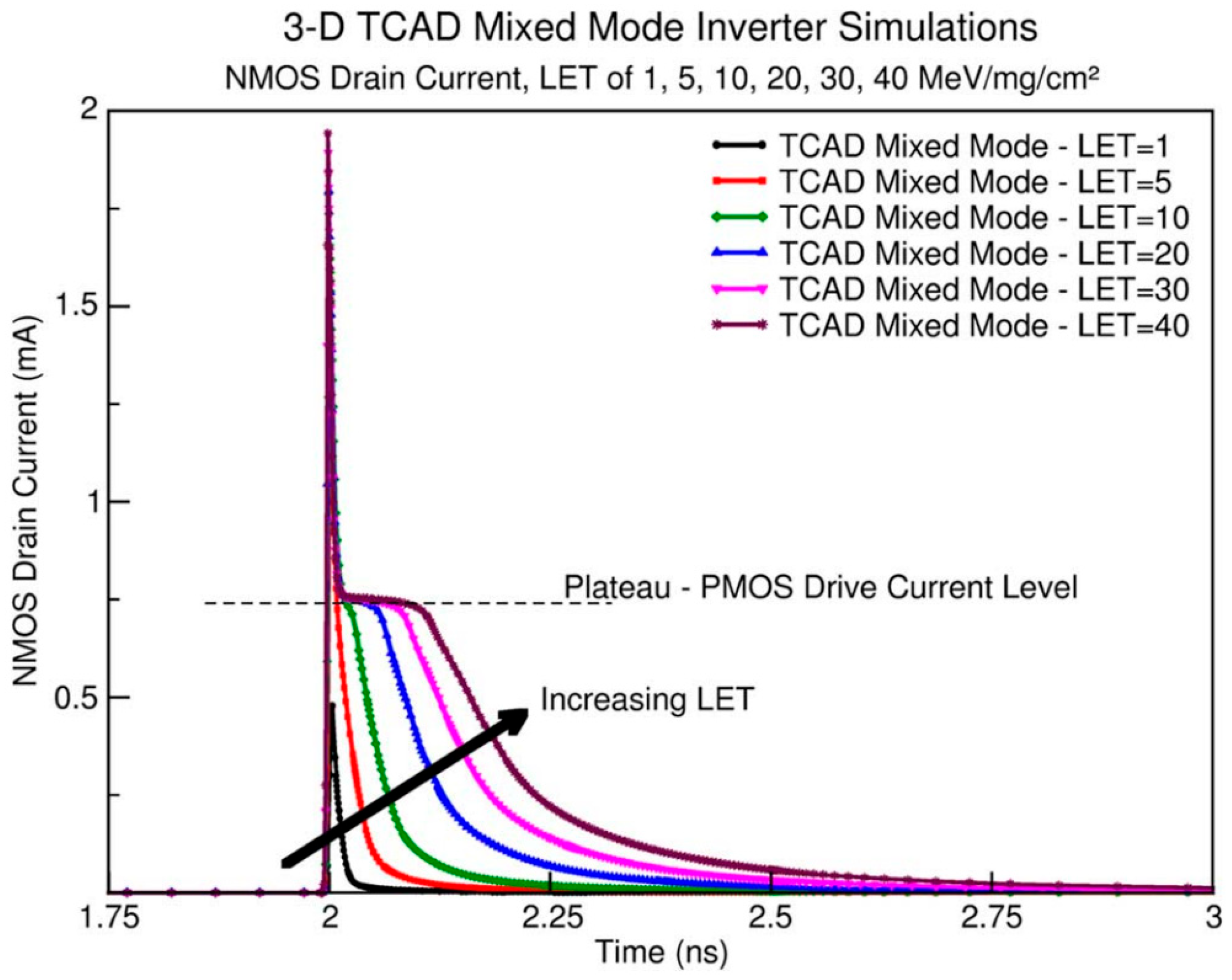
Although several studies have proposed extended models, such as the burst-plateau (BP) model [
26], that introduce a low-level current plateau after the initial transient (
Figure 8), this behavior is predominantly observed in bulk CMOS. In Fully Depleted SOI (FD-SOI), the reduced active silicon volume significantly limits sustained charge collection, making the plateau effect much less prominent, especially at lower LET values [
27]. For this reason and given that the purpose of pulse modeling in our work is to evaluate the circuit’s hardening response rather than replicate exact physical behavior, the DEF model is sufficient and appropriate.
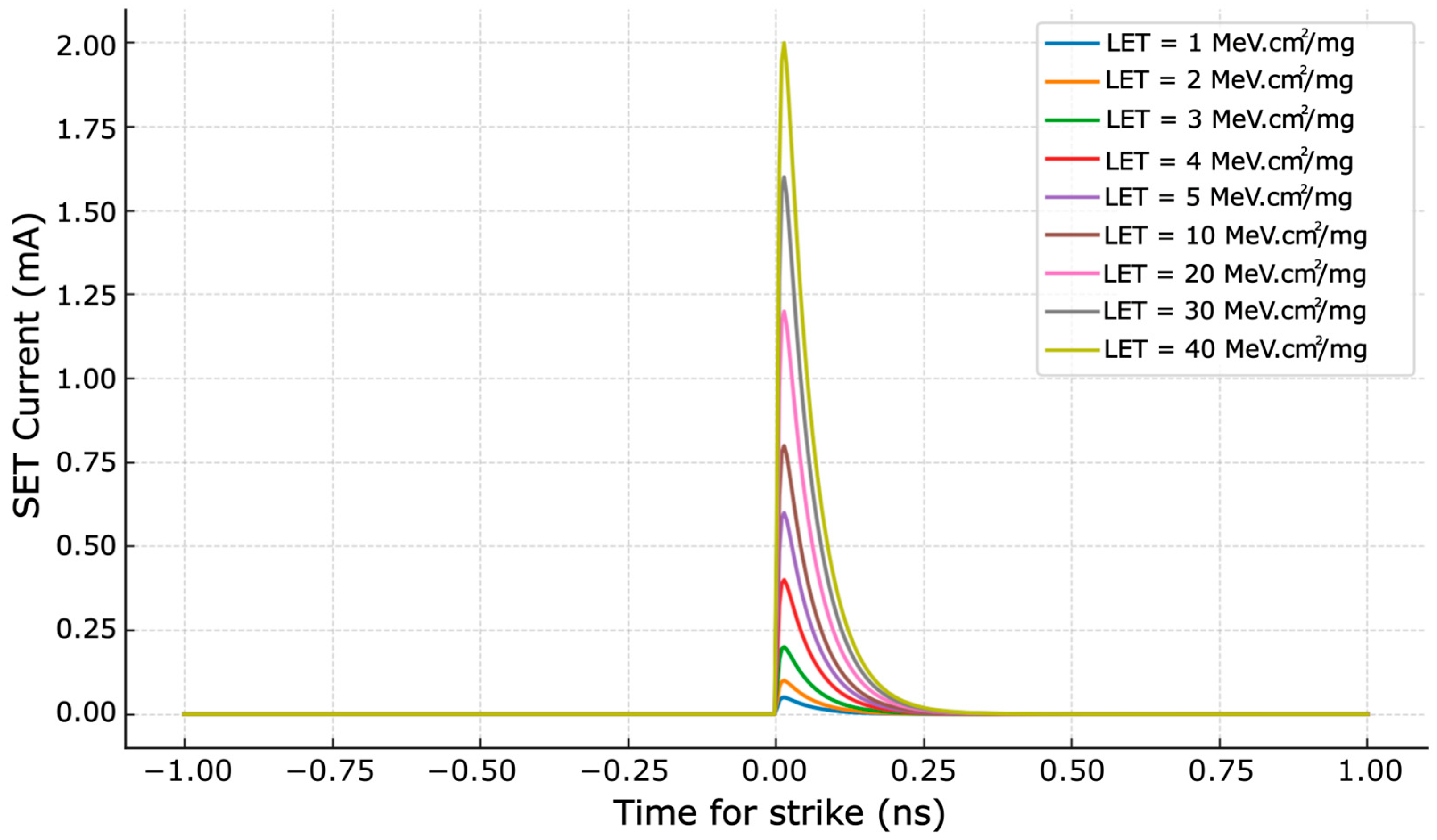
We implemented the SET current pulse using a Verilog-A behavioral model, integrated into Cadence simulations to inject transient faults at critical ADC nodes. The model parameters were calibrated against device-level TCAD results across multiple LET conditions. The simulated current pulses for LET values ranging from 1 to 40 MeV·cm
2/mg are shown in
Figure 9.
3.5. Scalability to Higher Resolutions
The proposed architecture can be extended to 6-bit and 8-bit flash converters. A flash ADC uses 2N −1 comparators. With sequential comparator activation, the average number of active comparators is ~2N−1; thus, dynamic power scales with the number of active comparators (roughly doubling per added bit), while area growth is dominated by the comparator array and thermometer latches. To manage power/area, a segmented-flash approach can reduce the effective comparator count while retaining the same hardening measures. The DMR-based detection/correction operates locally on thermometer latches, so its delay is set by the local logic and does not strongly depend on N. As resolution increases, the number of protected nodes grows; gating the checker with the enable chain and placing redundant nodes apart helps limit multi-bit upsets. Overall, the methods remain independent of ADC architecture and can be applied per segment or lane in higher-resolution designs.
3.6. Layout-Level Considerations
This work focuses on radiation hardening by design (RHBD); therefore, matching was a primary layout objective. Comparator input pairs, sampling capacitors, and reference-ladder elements were placed with common-centroid or interdigitated patterns, mirrored device orientation, and symmetric routing to minimize gradient-induced offset. Sensitive analog nets were kept short and routed away from fast digital lines to reduce coupling. Redundant thermometer-latch nodes used for DMR were placed with physical separation to limit charge sharing and lower the probability of multi-bit upsets. Local decoupling and robust supply routing were used to stabilize bias nodes and reduce supply-induced disturbances.
4. Simulation Results
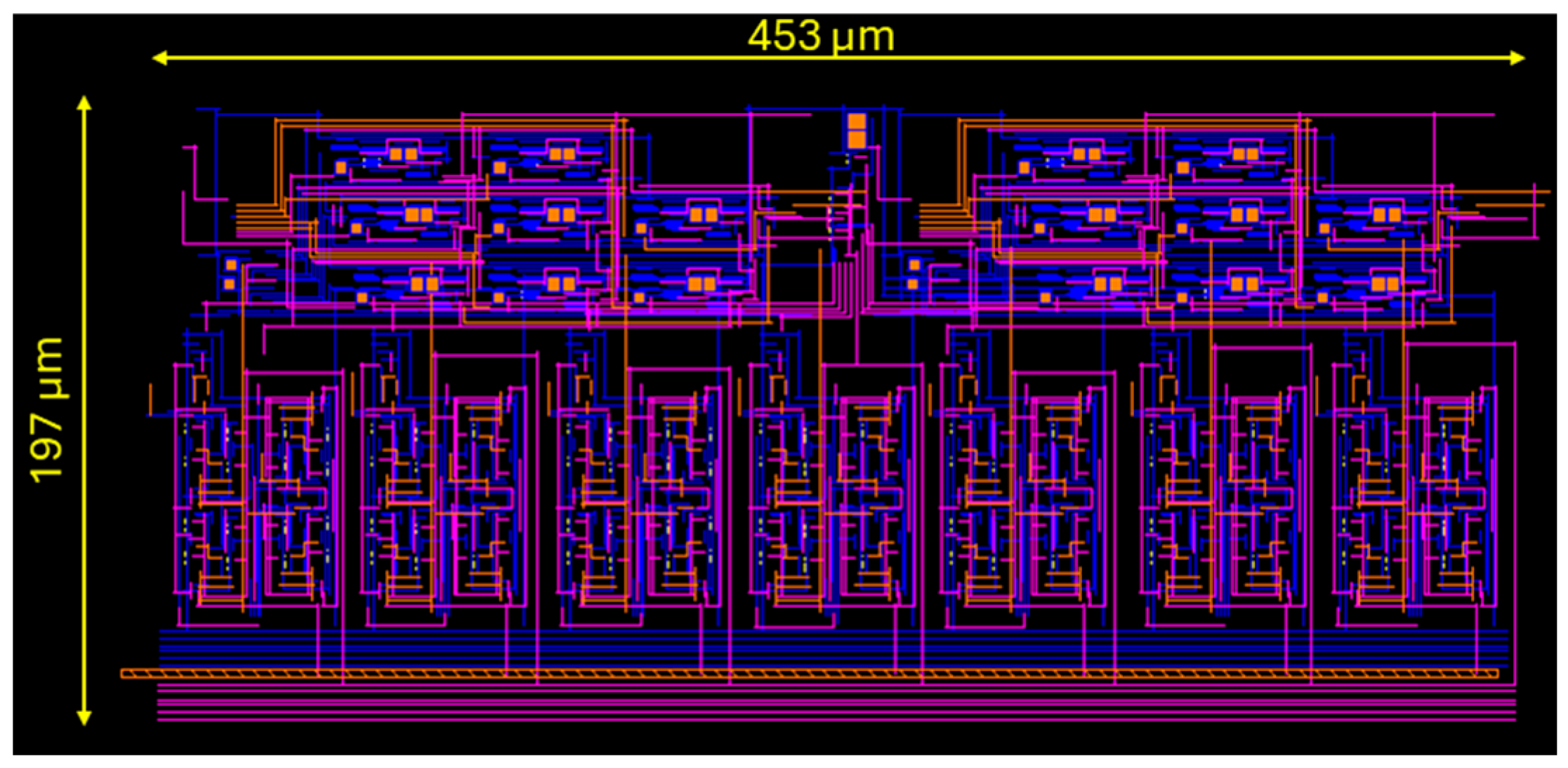
The proposed flash ADC was implemented in the GlobalFoundries 22 nm FD-SOI process.
Figure 10 shows the post-layout design, which occupies an active area of 0.089 mm
2. All simulations presented in this section were performed using post-layout extracted netlists.
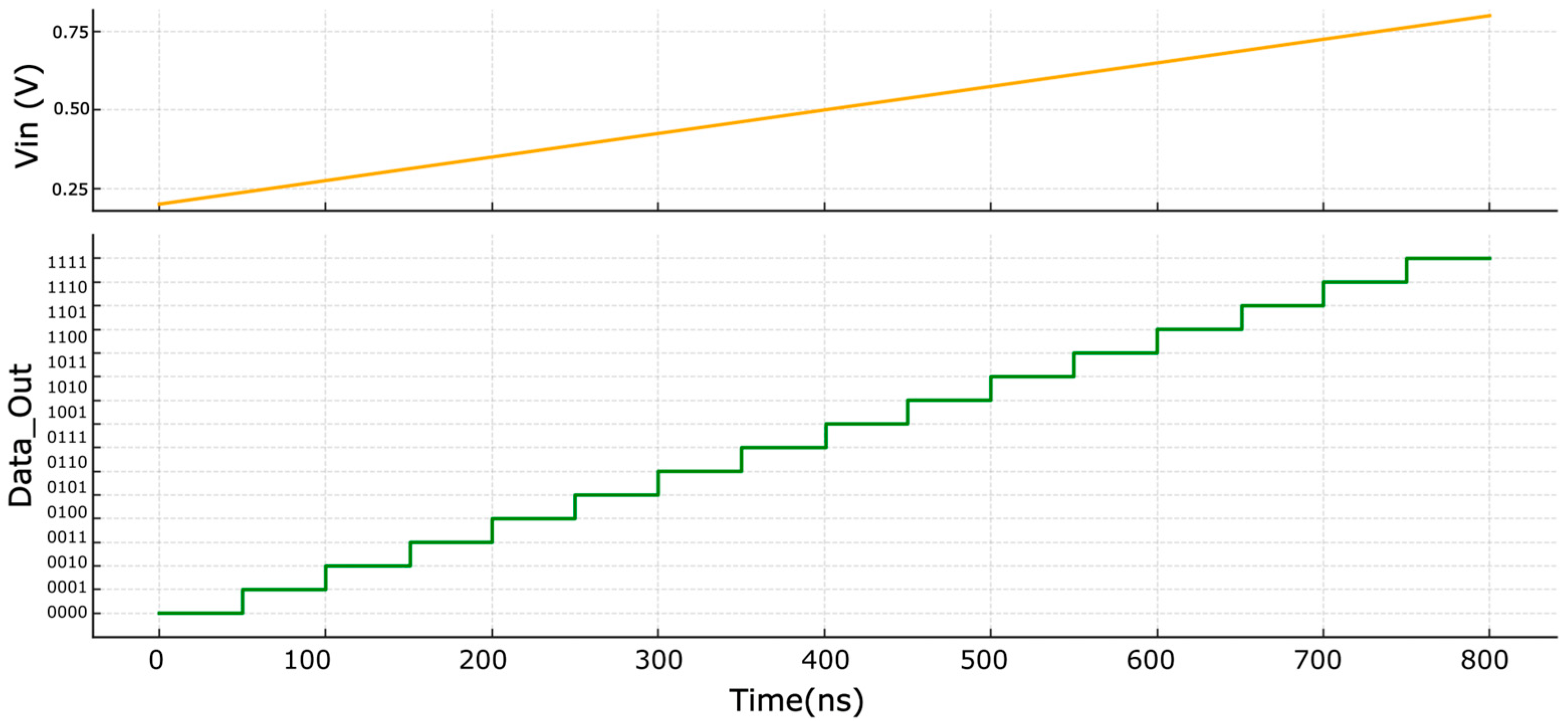
The proposed 4-bit flash ADC was simulated under nominal operating conditions for functional verification. The supply voltage was set to 1.0 V, with the reference ladder spanning 0.2 V to 0.8 V, providing a full-scale input range of 600 mV and an LSB step size of 37.5 mV. A linear input ramp from 0.2 V to 0.8 V was applied over 800 ns while the ADC operated with a 20 MHz sampling clock.
The simulated output codes in
Figure 11 confirm correct functionality. The output increases monotonically from 0000 to 1111 with no missing codes or reversals, including with a ±10% change in supply voltage (VDD). Each code transition occurs at the expected threshold set by the reference ladder, validating the comparator operation and the encoder mapping.
To evaluate the radiation resilience of the proposed ADC, single-event transient (SET) pulses were injected into critical nodes using the Verilog-A current source model described in
Section 3.4. Simulations were conducted across multiple Linear Energy Transfer (LET) values, with the pulse parameters extracted from a TCAD simulation of the 22 nm FD-SOI process.
SETs were applied to both analog-critical nodes (comparator input and bias network) and digital-critical nodes (thermometer-code latches). In the analog domain, the comparators maintained correct decision outputs for LET values up to 30 MeV·cm2/mg, beyond which transient shifts in decision threshold began to appear. In the digital domain, the XOR-based error detection circuit reliably identified upset events in the main data latch when Q exceeded the critical charge, generating a restore pulse to copy the safe value from the backup latch. At nominal conditions (25 °C, VDD = 1.0 V), fault detection was completed within 200 ps, and correction was finalized within 600 ps. When an upset occurred only in the backup latch, no restoration was triggered. Simultaneous upsetting of both latches resulted in an unrecoverable error.
Figure 12 shows an example simulation where an SET pulse was injected at the main latch output. The upper trace shows the error correction pulse generated in response to a detected error, the middle trace shows the corrupted Q output of the main latch before and after correction, and the lower trace shows the safe copy of the output bit. SEU recovery simulations were run at T = −40, 25, and 125 °C and VDD = 0.9, 1.0, and 1.1 V.
Table 1 summarizes the detection and correction times across these corners. The worst cases are about 275 ps for detection and 790 ps for correction at VDD = 0.9 V and 125 °C.
A linear input ramp was used to evaluate integral non-linearity (INL) and differential non-linearity (DNL) of the ADC across all corners. The maximum DNL was within ±0.4 LSB, while the maximum INL remained within ±0.3 LSB, demonstrating stable static performance of the converter.
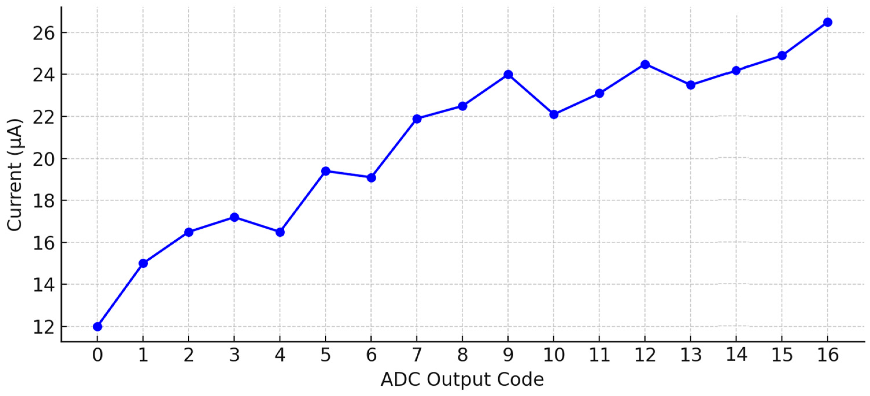
The static and dynamic current consumption of the ADC was measured across all output codes to evaluate power requirements under nominal conditions. A 1.0 V supply was used for all measurements. The results, shown in
Figure 13, indicate that the supply current varies with output code due to switching in the comparator array, encoder, and error-correction logic. The measured current consumption ranges from approximately 12 µA at code 0000 to 26.5 µA at the maximum code. This variation reflects the sequential comparator enable scheme, where higher codes activate more comparators, resulting in higher dynamic current. At 1.0 V, the corresponding power consumption ranges from 12 µW to 26.5 µW.
