1. Introduction
Driven by the requirement of improving aircraft efficiency, reducing fuel consumption, and greenhouse gas emissions, there is a growing trend to electrify the aircraft power system [
1,
2,
3]. This pushes research toward the continuous development of more electric aircraft (MEA) techniques that aim to replace the conventional mechanical, pneumatic, or hydraulic system with an electrical power system [
3]. Moreover, the hybrid and all-electric aircraft (HEA/AEA), which electrify the aircraft propulsion system and auxiliary power unit, can further improve the propulsive efficiency, and reduce carbon emissions and acoustic noise [
3,
4]. For the implementation of electrified aircraft, protection is a critical challenge to ensure safety and reliability.
Highly electrified aircraft normally utilize a power electronic converter-based HVDC power distribution system since it can reduce the cable weight and cost [
5,
6,
7]. However, the HVDC system suffers from high fault current magnitude and rise rate due to the large DC-link capacitors and low fault impedance. Therefore, fast fault interruption is required to constrain the fault current and, consequently, protect the power electronic devices, which have limited surge capability, from being destroyed by overheating.
A conventional electromechanical circuit breaker (ECB), whose interruption time is around tens of milliseconds or more, cannot satisfy the protection requirement of power electronic devices in HVDC system [
8]. Furthermore, the lack of zero crossing points in DC current may also accelerate the ECB contact corrosion speed. Therefore, solid state power controllers (SSPCs) have gained popularity in aircraft HVDC systems, considering the advantage of no mechanical moving contacts and arc-less current interruption capability with fast protection time.
The continuously climbing power level of the aircraft HVDC system requires the circuit breaker (CB) to have higher current interruption capability. However, the existing SSPCs only have limited capacity and can only be utilized in the aircraft secondary power distribution systems. Although companies like Data Device Corporation (DDC) [
9], Sensitor [
10], and HYJAS Electronics [
11] have already released 270 V DC SSPC products, the maximum rated current is only 150 A, which cannot meet the requirement of the future electrified aircraft.
In the academic area, challenges like current balancing, transient voltage mitigation, and transient thermal modeling have been extensively investigated. In [
12], a double edge modulation-based control strategy is proposed to decrease the d
i/d
t during switching transients. However, the interruption current is only 40 A, and the proposed strategy can lead to intermittent output voltage during switching. Metal oxide varistor (MOV) combined with snubber capacitor are dedicatedly designed and utilized as a transient voltage absorption circuit in [
13], and the rated/interruption current reaches 100 A/150 A under the condition of 20 μH power loop parasitic inductance. However, MOV suffers from degradation issues and is not suitable for aircraft applications. In [
14], a transient voltage suppressor (TVS) array-based peak voltage clamp circuit, which can achieve faster response speed and lower clamping ratio without degradation issue, is proposed. Although the nominal current is increased to 350 A, the maximum interruption current is only 1.3 times the rated current (450 A). Furthermore, the parallel connection of TVSs may cause current imbalance due to differences in clamping characteristics.
To further increase the SSPC power capacity, parallel connection of the switching devices is inevitable considering the insufficient current rating. Active current sharing [
15,
16], which actively regulates the drive signals of parallel devices to mitigate the current imbalances caused by power loop parasitic parameters, has been proposed. However, since active current balancing methods commonly rely on dedicatedly designed gate drive circuits [
17] and require multiple switching cycles for closed-loop current compensation [
18,
19], it is not suitable for SSPC applications where the power devices do not operate in continuous switching operation. It is worth noting that an active gate driver proposed in [
20] utilizes a differential mode choke to achieve current sharing within a single switching cycle. However, the complexity introduced by this approach makes the driver circuit difficult to implement, particularly when paralleling more than two power devices. Consequently, passive current sharing methods are the preferred and more suitable approach for SSPC designs. These methods offer inherent current balancing without the need for a complex driver circuit, control algorithms, or multiple switching cycles, aligning well with the operational requirements of SSPCs [
21]. A symmetrical circle layout is proposed with the maximum interruption current increases to 1.1 kA [
22]. However, the independent heat sink required by each parallel MOSFET significantly complicates the physical and air duct design, and thus makes the method difficult to apply in practical applications. By utilizing two SiC MOSFET modules in series with liquid cooling system, the interruption current can be increased to 1.8 kA with 8 μH power loop parasitic inductance [
23]. However, the high cost of the power modules and the limited availability of liquid cooling systems restrict their widespread adoption in aircraft applications. By utilizing two GaN devices in parallel, a 750 V/100 A SSPC is proposed in [
24]. This work, however, does not address the current balancing issue, and the reliance on a cryogenic cooling system further limits its practical application. The performance and key characteristics of the aforementioned SSPC designs are listed in
Table 1.
To summarize, current research on SSPCs primarily focuses on achieving manufacturing maturity for devices exhibiting high power density, superior protection performance, and high efficiency across diverse applications. However, the existing literature still lacks comprehensive research on high-power, low-cost, and easily integrated SSPCs. Addressing these challenges, this paper proposes a passive current balancing strategy based on an irregular-shaped power busbar and a TVS-based peak voltage mitigation strategy, alongside a comprehensive SSPC design procedure. Furthermore, the proposed SSPC requires only an air-cooling system, which simplifies the system physical structure and thus significantly extends its application range. Finally, the development of a 270 V/300 A DC SSPC prototype is presented.
The rest of the paper is organized as follows.
Section 2 explains the detailed operating principle and system design considerations while
Section 3 mainly discusses the switching device selection and the corresponding thermal design.
Section 4 analyzes the challenges of paralleling switching devices and gives the design guidelines of the proposed irregular-shaped busbar. In
Section 5, the design of the proposed RC-TVS clamping circuit is illustrated in detail. Experimental results are analyzed and discussed in
Section 6. Finally,
Section 7 presents the conclusion of the paper.
4. Passive Current Balancing Strategy
Passive current balancing methods can be categorized into three main types: pre-screening of power devices to minimize parameter mismatch, symmetrical PCB or circuit layout to equalize parasitic effects, and the incorporation of passive components such as resistors or inductors for current equalization. Considering that inserting passive components in series with the power loop can significantly increase system losses, volume, and weight, and that the previously proposed coupled-inductor-based current balancing method may introduce higher voltage spikes across power devices, these passive strategies are not suitable to be applied to high power SSPC applications.
The parasitic parameters of the power loop significantly impact current sharing performance among parallel devices. To address this issue, this paper proposes a compensation strategy for power loop parasitic components to optimize parameter imbalance across parallel branches. Note that device preselection is a straightforward and effective method for mitigating current imbalance; however, it is not discussed here as it has been well-addressed in the existing literature.
4.1. Determination of SSPC Architecture
For the purpose of achieving uniform thermal conditions and subsequent balanced current performance among the power devices, a single heat sink was utilized for the mounting of all components, and the 9 MOSFETs were divided into three power modules, each containing three parallel power devices as shown in
Figure 8.
4.2. Irregular-Shaped Busbar-Based Parasitic Parameter Compensation Strategy
By introducing strategic openings in the busbar, the impedance of the parallel branches is balanced. This principle of parasitic parameter compensation aims to mitigate the current imbalances caused by parasitic parameters of the parallel devices, thereby finally ensuring current balance.
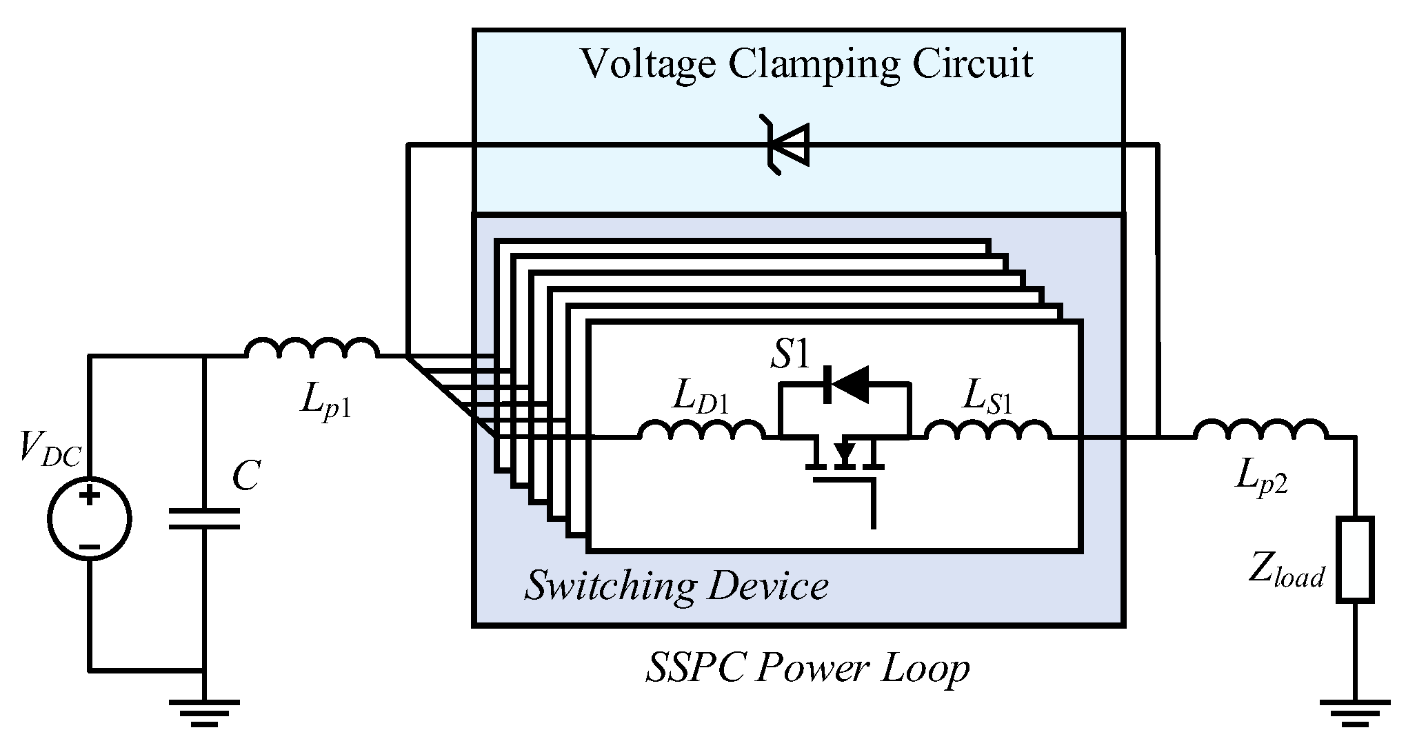
Figure 9 depicts the power circuit configuration of a single module, highlighting the change introduced by the busbar window opening. As shown, the window opening increases the length of the power loop for Device 2, leading to an increase in the parasitic parameters of that parallel branch.
4.3. Window Size Design of Busbar
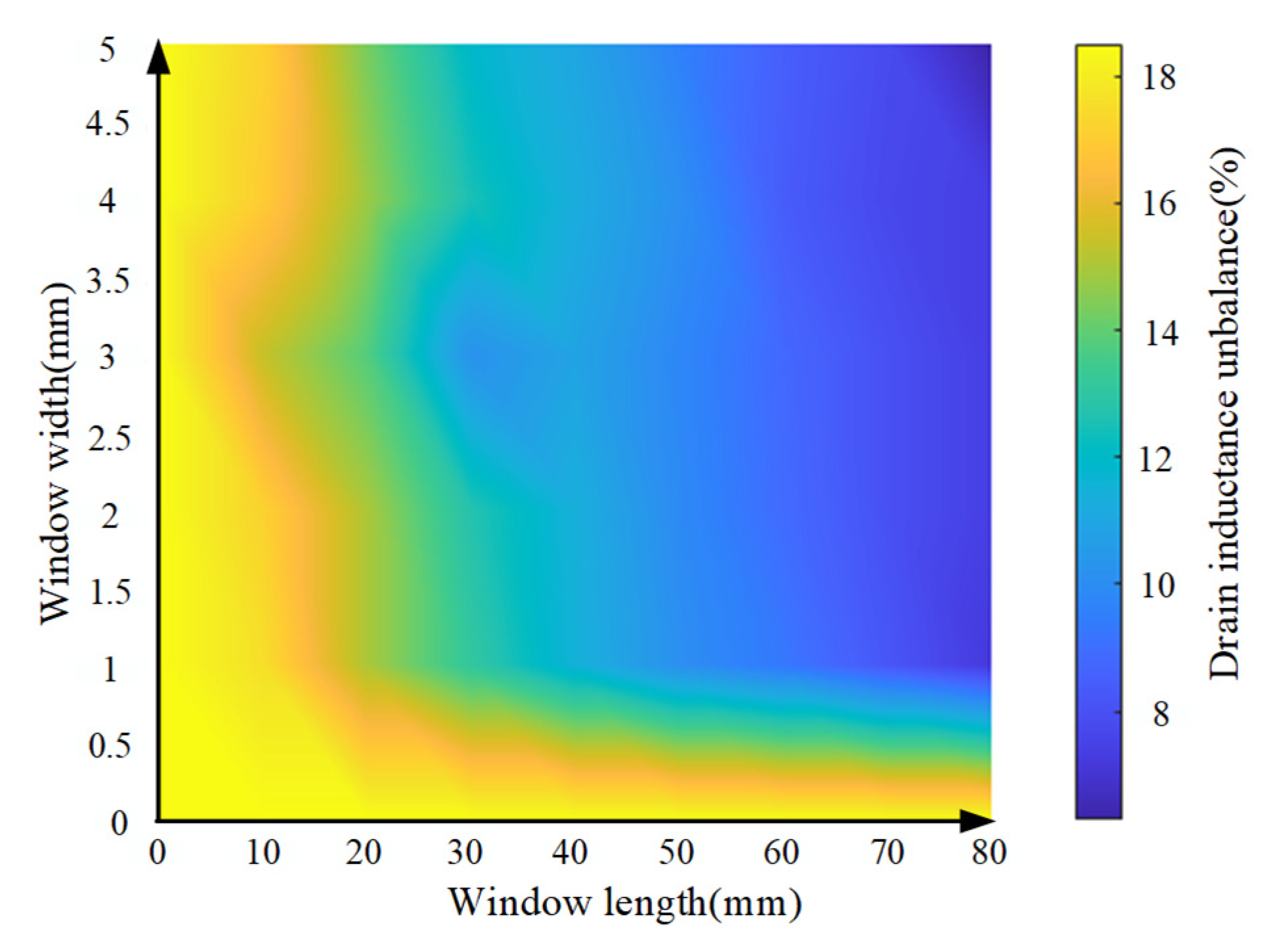
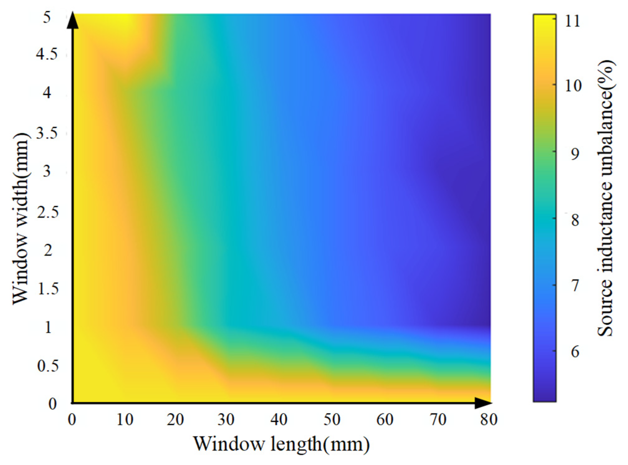
In order to analyze the influence of window size on the parasitic parameters of parallel branches, the busbar model is established, and the parasitic parameters of different power loops are extracted by utilizing ANSYS Q3D 2024 to analyze the variations of parasitic parameters under different window sizes. The relationships between window sizes and the different parasitic parameters are presented in
Figure 10,
Figure 11 and
Figure 12. The inductance and resistance unbalance are calculated according to the following equation.
where Δ
Xmax is the maximum difference of the inductance or resistance in the different branches, and
Xavg is the average of the inductance or resistance. Note that the window length varies from 0 mm to 80 mm, and the window width varies from 0 mm to 6 mm.
It can be seen from
Figure 10,
Figure 11 and
Figure 12 that with the increase of the window area, the imbalance of drain inductance, source inductance, and loop resistance decreases. Conversely, a larger window area forces the current to flow around a larger effective loop, increasing the loop self-inductance by allowing more magnetic flux to pass. Simultaneously, this larger window size reduces the effective conductive cross-sectional area and increases the current path length, thereby increasing the loop resistance. Consequently, the window size is finally designed as 80 mm and 4 mm, respectively, to provide a compromise between current balancing performance, power loss, and transient performance characteristics. The inductance and resistance matrix of the designed busbar are shown in
Table 7 and
Table 8.
In the inductance matrix presented in
Table 7, the diagonal elements represent the self-inductance of each branch, while the off-diagonal elements represent the mutual inductance among the branches. Based on the inductance matrix and the resistance matrix, the calculated unbalance factors for drain inductance, source inductance, and total branch resistance are 7.4%, 5.3%, and 1.6%, respectively. These values indicate a low level of impedance unbalance.
4.4. Simulation Results
The extracted parasitic parameters were used in LTspice to simulate current balancing. The simulation results are shown in
Figure 13.
The current unbalance factor during both switching and steady-state operation, calculated from the simulation results, is presented in
Table 9. As demonstrated by the results, the current unbalance factor remains below 5% under both operating states, provided that the devices have consistent parameters and no other supplementary current balancing techniques are employed. Note that the current unbalance factor is calculated using the following equation:
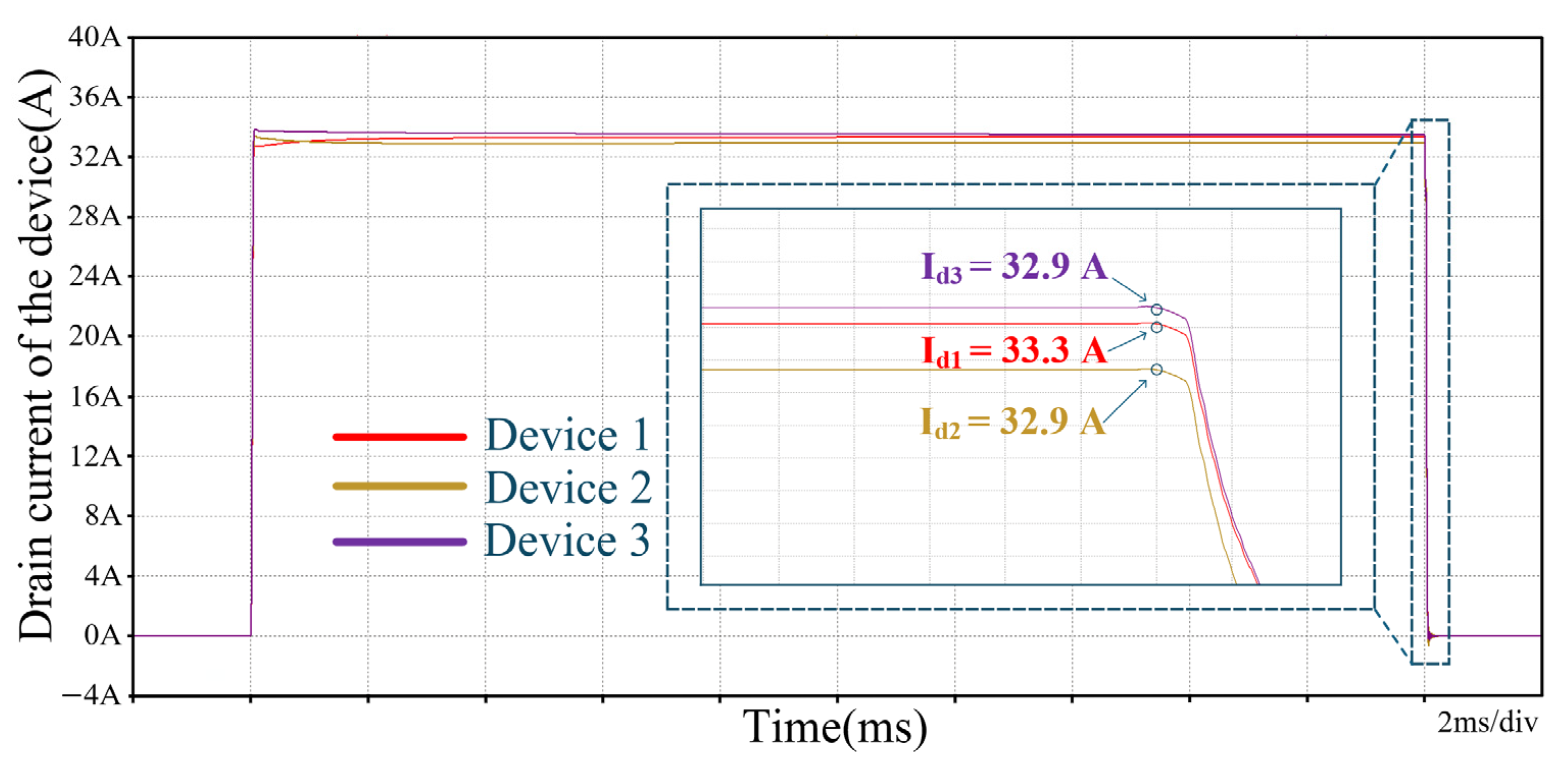
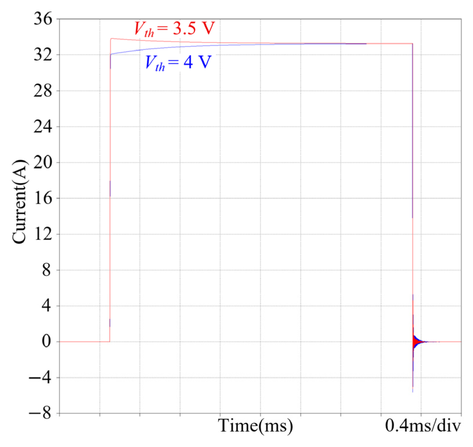
Furthermore, a single-parameter sensitivity analysis was conducted to evaluate parameter spread effects on current sharing in the parallel devices. Based on the device datasheet, Rdson ranges from 6.7 mΩ (typ) to 9 mΩ (max), threshold hold voltage Vth varies between 3.0–4.0 V, and a conservative 10% Qg variation was assumed due to unspecified tolerance.
The analysis varied each parameter to its maximum value in one of three parallel devices while maintaining identical circuit parasitics. As shown in
Figure 14,
Figure 15 and
Figure 16, current unbalance factors reach 19.5% for
Rdson variation, 0.2% for
Qg variation, and 5.3% for
Vth variation.
Rdson variation dominates steady-state performance with negligible transient impact. Lower
Vth causes earlier turn-on and higher transient current amplitude but minimal steady-state effect due to current convergence.
Qg variation shows a similar trend with substantially lower impact.
5. Voltage Spike Suppression Circuit Design
During the SSPC turn-off process, the high di/dt in the main power loop induces a voltage spike across the parasitic inductance, potentially exceeding the breakdown voltage of the power device. A common method to absorb the energy stored in this parasitic inductance is to connect a MOV or TVS in parallel with the power device; TVSs are preferred in this paper due to their faster response speed and lower clamping voltage compared to MOVs, which are susceptible to aging with repeated operation. However, the parasitic inductance associated with the TVS branch can generate additional voltage spikes during SSPC turn-off, further increasing the voltage stress on the power device. To effectively mitigate these voltage spikes, an RC-TVS-based voltage spike suppression circuit is proposed.
5.1. The Cause of Voltage Spikes
The specific operation process during SSPC turn-off is detailed below, with the corresponding typical waveform shown in
Figure 17.
t0–t1: At t0, when a short circuit occurs, the SSPC current (ISSPC) rapidly rises, and the power device drain-source voltage (vDS) increases slightly.
t1–t2: At t1, ISSPC reaches its short-circuit protection threshold, initiating the turn-off of the power device. As the power device turns off, the current is commutated to the TVS branch, causing the power device current (iD) to decrease and the TVS current (if) to increase. Consequently, the drain-source voltage (vDS) rises rapidly until the TVS breaks down. Following this rapid current commutation between the main power circuit and the TVS branch, the power device current (iD) finally drops to zero at t2, at which point the TVS enters its reverse stand-off state.
Based on the above-mentioned analysis, during SSPC turn-off, the fault current commutates from the power device to the TVS. This rapid current change (high d
if/d
t) generates an overvoltage (
vST) across the parasitic inductance (
LST) of the TVS branch. The relationship between
vST, the TVS clamping voltage (
vC), and the voltage across the power device (
vDS) can be expressed as:
It can be seen from (12) that the power device must withstand the sum of the voltage across the TVS branch parasitic inductance and the TVS clamping voltage during the turn-off process. Furthermore, high-power TVSs often exhibit a foldback characteristic, where the initial breakdown voltage is higher than the average clamping voltage. This foldback effect also contributes to an initial voltage overshoot at the beginning of SSPC turn-off. Based on this analysis, this paper proposes the integration of an RC snubber circuit to limit the rate of current change (di/dt) and effectively suppress the voltage spike during the initial phase of the turn-off process.
5.2. TVS Foldback Characteristics
The initial voltage spike during SSPC turn-off is composed of the clamping voltage and the voltage across the line inductance. A key consideration for high-power TVSs is their foldback characteristic [
28], which significantly influences this initial spike. This characteristic, a common design in high-power TVSs with smaller die sizes to absorb high-peak pulse currents, exhibits a higher clamping voltage at the onset of breakdown. This temporary increase in clamping voltage is intentionally designed to quickly suppress overvoltage before the voltage is reduced to a lower level to limit power dissipation and avoid thermal runaway during sustained clamping.
Figure 18 presents the surge response curve of a high-power TVS, illustrating its characteristic foldback behavior. This characteristic is further evident in the SSPC turn-off waveform shown in
Figure 17, where the voltage across the TVS terminals (
VC_FB) at the beginning of breakdown is observed to be higher than the average clamping voltage (
VC_AVG). This initial voltage peak is an inherent consequence of the foldback characteristic designed into high-power TVSs. As this characteristic is prevalent in high-power TVS products from leading manufacturers like Littlefuse and Bourns, mitigating the resulting voltage peak during SSPC operation when using these devices as clamping elements poses a significant challenge.
5.3. RC-TVS Parametric Design
In the proposed RC-TVS circuit, the TVS serves as the primary energy absorption component, while the RC snubber circuit, connected in parallel with the TVS, is implemented to mitigate the rate of current change (d
i/d
t) during the turn-off process. The buffer capacitance (
CS) can be estimated based on the buffer time (Δ
tC), TVS clamping voltage (
vC), and short-circuit current (
iSC), as expressed by the following equation:
where Δ
tC is the duration that the device drain-source voltage
vDS rises from 10% to 90% to its maximum. The current change rate and response speed are tested experimentally to meet the performance requirements of SSPC in this paper.
The buffer resistor serves the dual purpose of suppressing displacement current during SSPC turn-on and ensuring an overdamped RLC loop. Therefore, the buffer resistance value must satisfy the constraints shown in Equation (14).
When selecting the TVS diode, the key parameters to determine are the maximum reverse working voltage (VRWM), the breakdown voltage (VBR), and the peak clamping voltage (VC). The breakdown voltage (VBR) must be greater than the maximum bus voltage (VBUS) to avoid unwanted breakdown during normal operation. Conversely, the peak clamping voltage (VC) must be lower than the maximum breakdown voltage (VDS) of the protected device to ensure its safe operation during transient events.
To provide reliable overvoltage protection for the power device, the TVS peak clamping voltage (
VC) should be chosen to be 10% lower than the power device rated voltage (
VDS(rate)). Simultaneously, to prevent significant leakage current in the TVS during normal operation, its maximum continuous reverse working voltage (
VM(DC)) should be 10% higher than the DC bus voltage (
VBUS). Then, the voltage selection criteria for the TVS are summarized in (15).
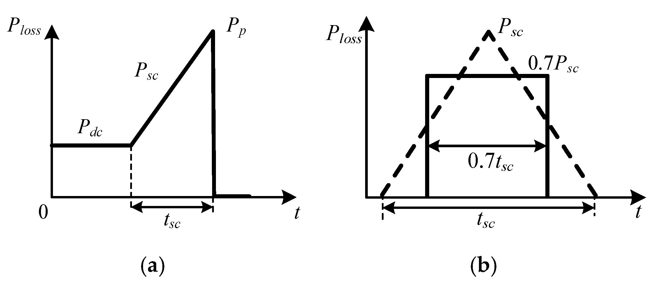
Moreover, to calculate the power dissipation in the TVS during a fault, the duration of the current pulse must be determined. This pulse width can be derived from the current waveform experienced by the TVS during the protection process in an ideal scenario. Considering that the TVS current typically exhibits an exponential decay, whereas the initial fault current can be modeled as a sawtooth, an appropriate conversion is required to find the equivalent pulse width under the exponential waveform for accurate power rating calculation. Equation (16) provides the formula for the converted pulse width.
where
LSTRAY is parasitic inductance, and
tPE is the equivalent pulse duration. The selection of an appropriate TVS requires considering its peak pulse current (
IPP) and peak pulse power (
PPP) capabilities, both of which are related to the current pulse width determined by equation (16). For reliable protection during a short circuit, the TVS must be able to handle the SSPC peak short-circuit current (
ISC) and peak short-circuit power (
PSC), as indicated by the conditions in (17) and (18). Note that
IPP and
PPP of the TVS for a given pulse width can be found on the peak pulse power derating curve in its datasheet.
Based on the preceding analysis, the TVS selection procedure can be summarized as follows: First, determine the voltage ratings of the TVS. The breakdown voltage should be greater than the system nominal voltage (270 V), and the peak clamping voltage should be less than the maximum rated drain-source voltage of the protected device (650 V). Secondly, assuming a TVS clamping voltage of 450 V, the current pulse widths are calculated using Equation (16) as tP1 = 142.9 µs and tP2 = 47.6 µs. Based on these pulse widths, the TVS must be capable of withstanding a peak pulse current of 1800 A (corresponding to tP1 = 142.9 µs) and a peak pulse power of 270 kW (corresponding to tP2 = 47.6 µs). These conditions ensure the selected TVS provides effective overvoltage protection for the SSPC.
In this paper, the KC380 TVS diode from DOWOSEMI is selected. Its specifications include a maximum reverse working voltage of 380 V, a minimum breakdown voltage of 401 V, and a peak clamping voltage of 520 V under an 8/20 µs pulse. The peak pulse current rating is 10 kA for an 8/20 µs pulse, which is derated to 7.5 kA under the same 8/20 µs pulse at an ambient temperature of 60 °C.
6. Experimental Verification
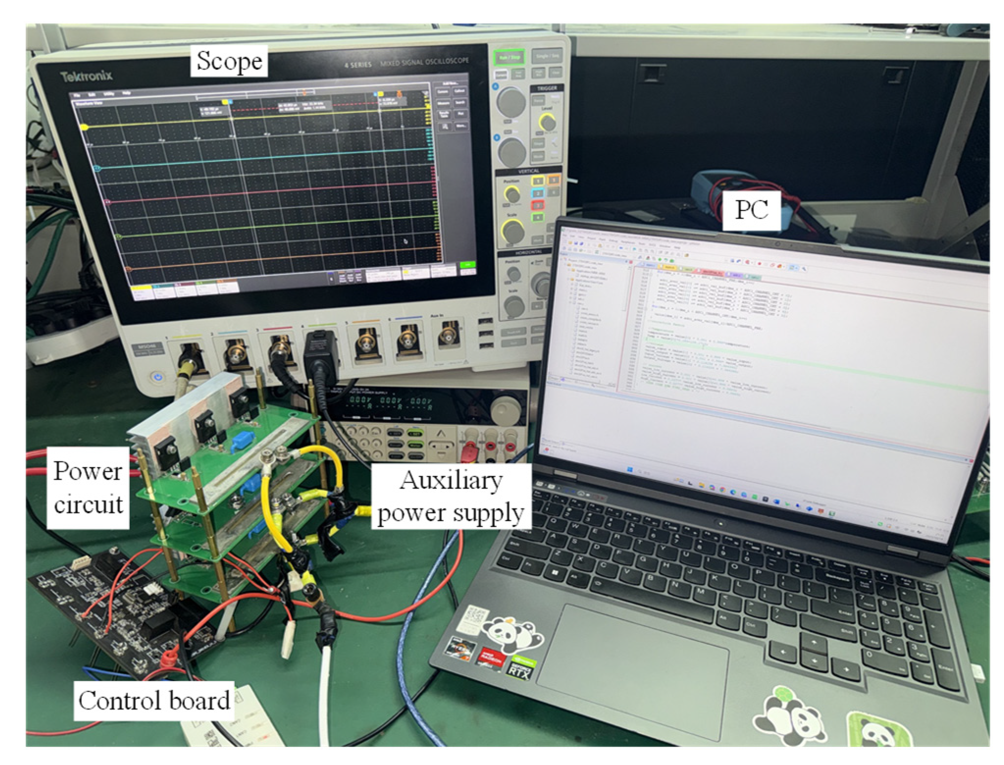
To validate the effectiveness of the proposed passive current sharing strategy and the RC-TVS voltage spike suppression strategy, a 270 V/300 A SSPC prototype was built in this paper, as shown in
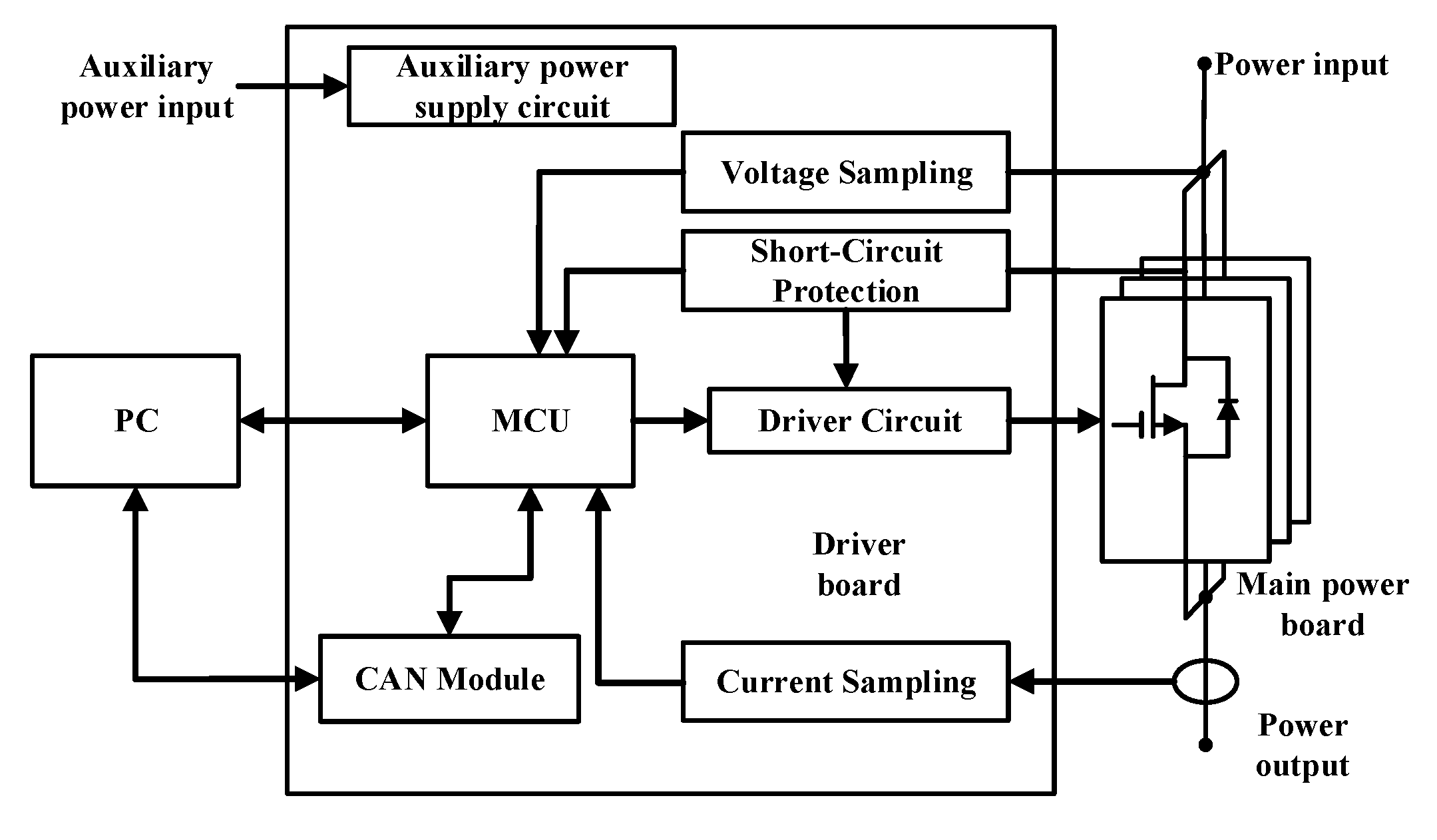
Figure 19. The prototype consists of a control circuit and a power circuit. The control circuit incorporates an MCU minimum system, a driver circuit, a short-circuit protection circuit, a sampling circuit, an auxiliary power supply circuit, and a CAN communication circuit. The power circuit features 9 power devices, the designed irregular-shaped busbar, and the RC-TVS overvoltage mitigation circuit.
The implemented design utilizes the Qorvo UF3SC065007K4S SiC FET featuring a Kelvin source pin, driven by an Infineon IED3124MU12FXUMA gate driver IC (200 kV/μs common-mode transient immunity). With a peak output current of 14 A, the driver supplies approximately 1 A per channel under the configured turn-on gate resistance of 18.5 Ω. This single-driver configuration effectively controls all nine parallel MOSFETs while minimizing inter-device switching delays, thereby improving current sharing performance. For protection, a shunt resistor [
29] enables overcurrent and short-circuit detection with a measured response latency of around 500 ns.
6.1. SSPC Switching Test
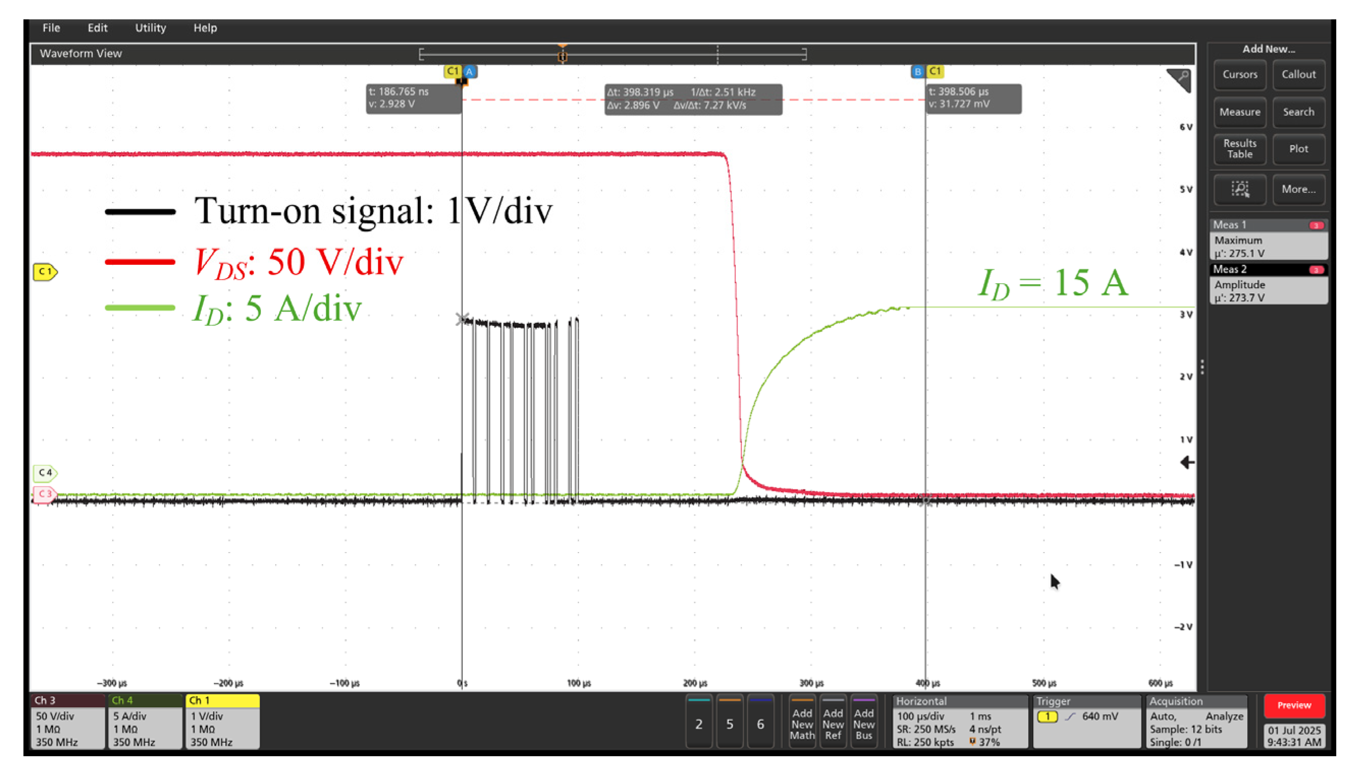
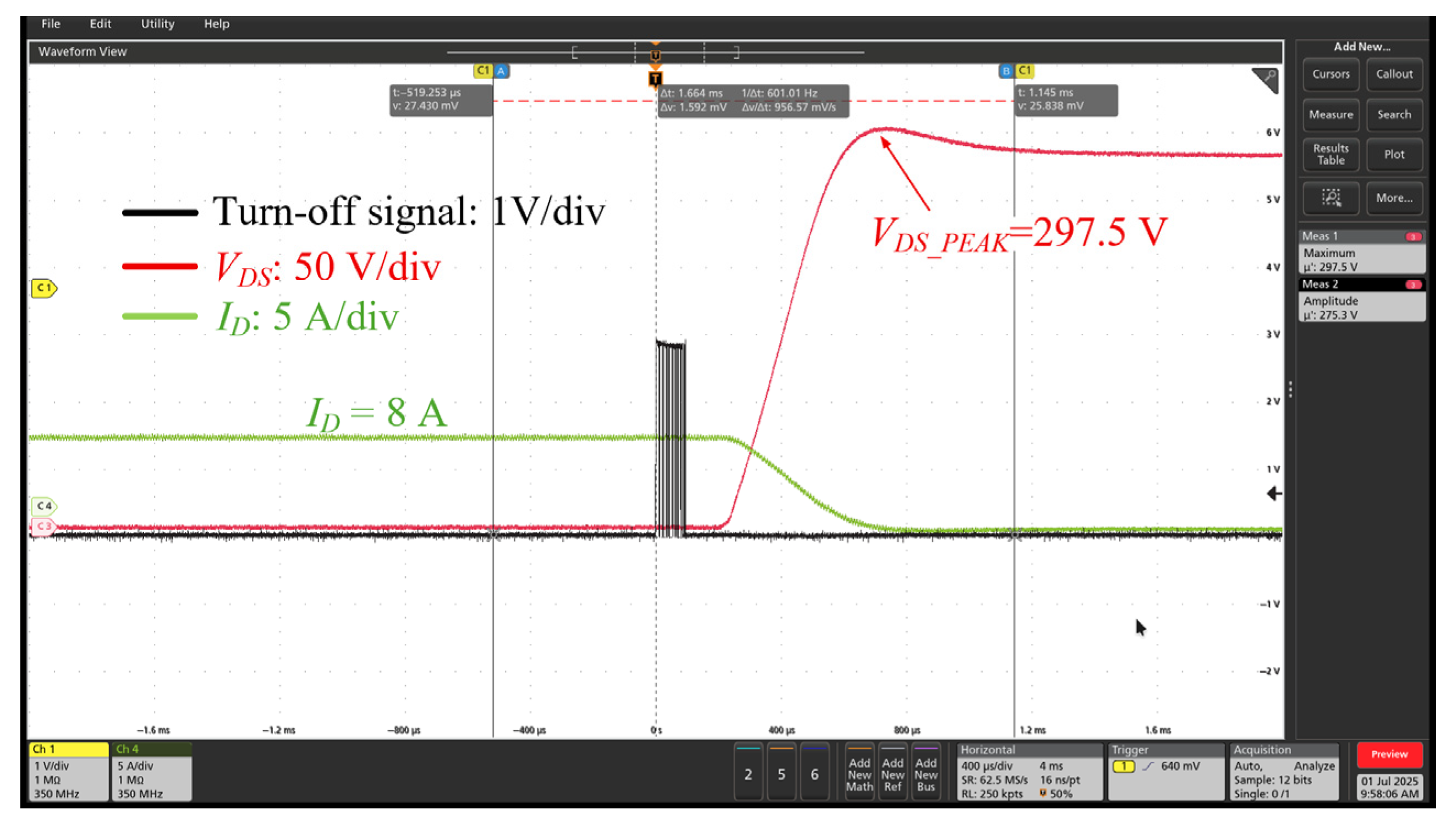
The switching transient performance of the SSPC was investigated under conditions of 270 V DC bus voltage and a resistive load. The measured voltage and current waveforms during turn-on and turn-off are presented in
Figure 20 and
Figure 21, respectively. A noticeable voltage overshoot is observed during turn-off, where the peak voltage reaches 297.5 V. Note that the black trace represents the turn-on and turn-off signals received via communication.
6.2. Current Balancing Experiment
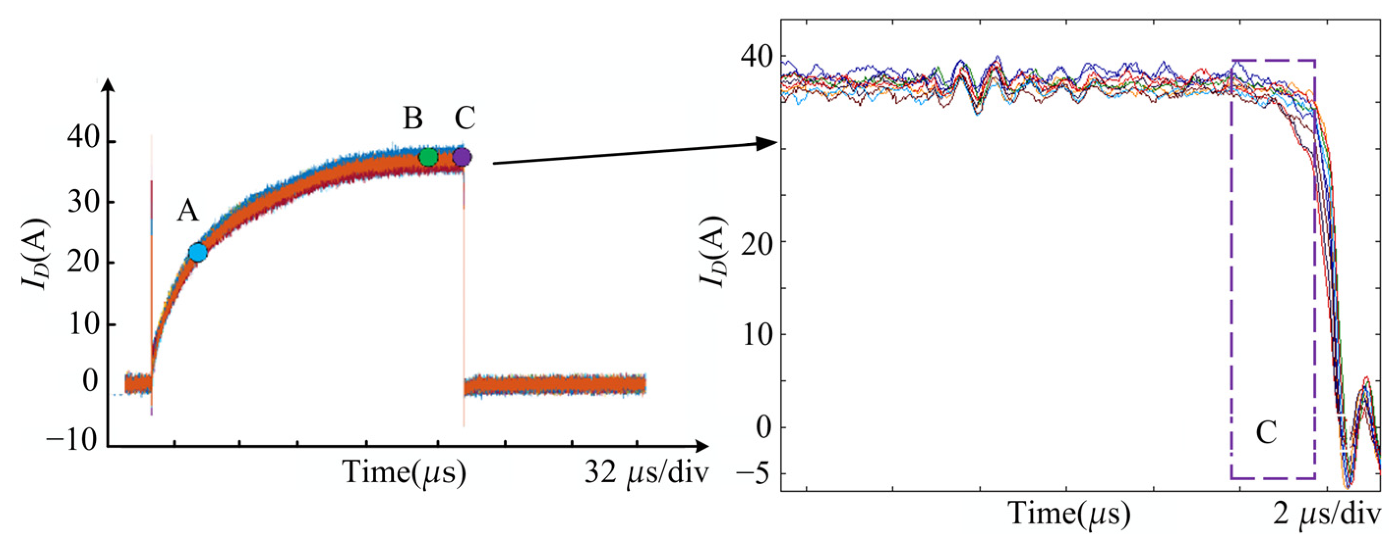
Figure 22 shows the current waveforms of the nine parallel power devices operating under a 300 A load. Analysis of these waveforms, following Equation (11), reveals a steady-state current balancing unbalance factor of 4.2%. The dynamic current balancing unbalance factor is 2.2% during turn-on and 7% during turn-off, respectively. These results indicate that the current sharing among the parallel devices is satisfactory. Note that the current unbalance factor during turn-on, steady-state, and turn-off is measured at points A, B, and C, respectively.
6.3. Overvoltage Suppression Effect of RC-TVS
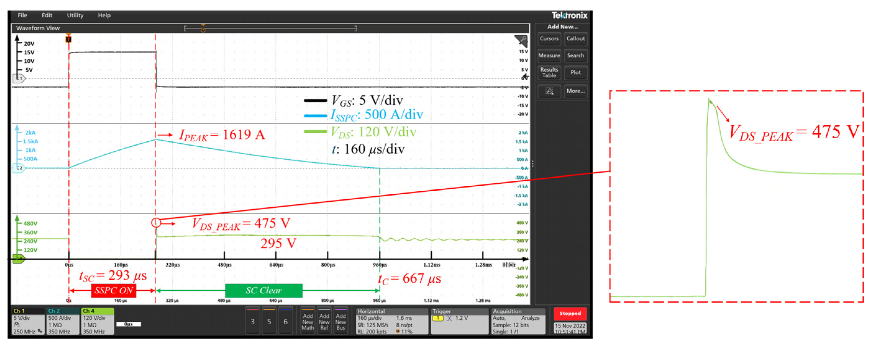
Figure 23 illustrates the experimental waveform obtained under a fault current of 1.6 kA and a parasitic inductance of 40 μH. The waveform shows that the peak voltage across the power device reached 475 V, while the clamping voltage provided by the RC-TVS circuit was 295 V. These results demonstrate the effectiveness of the proposed RC-TVS circuit in suppressing overvoltage during the SSPC turn-off process.
6.4. Short-Circuit Experiment
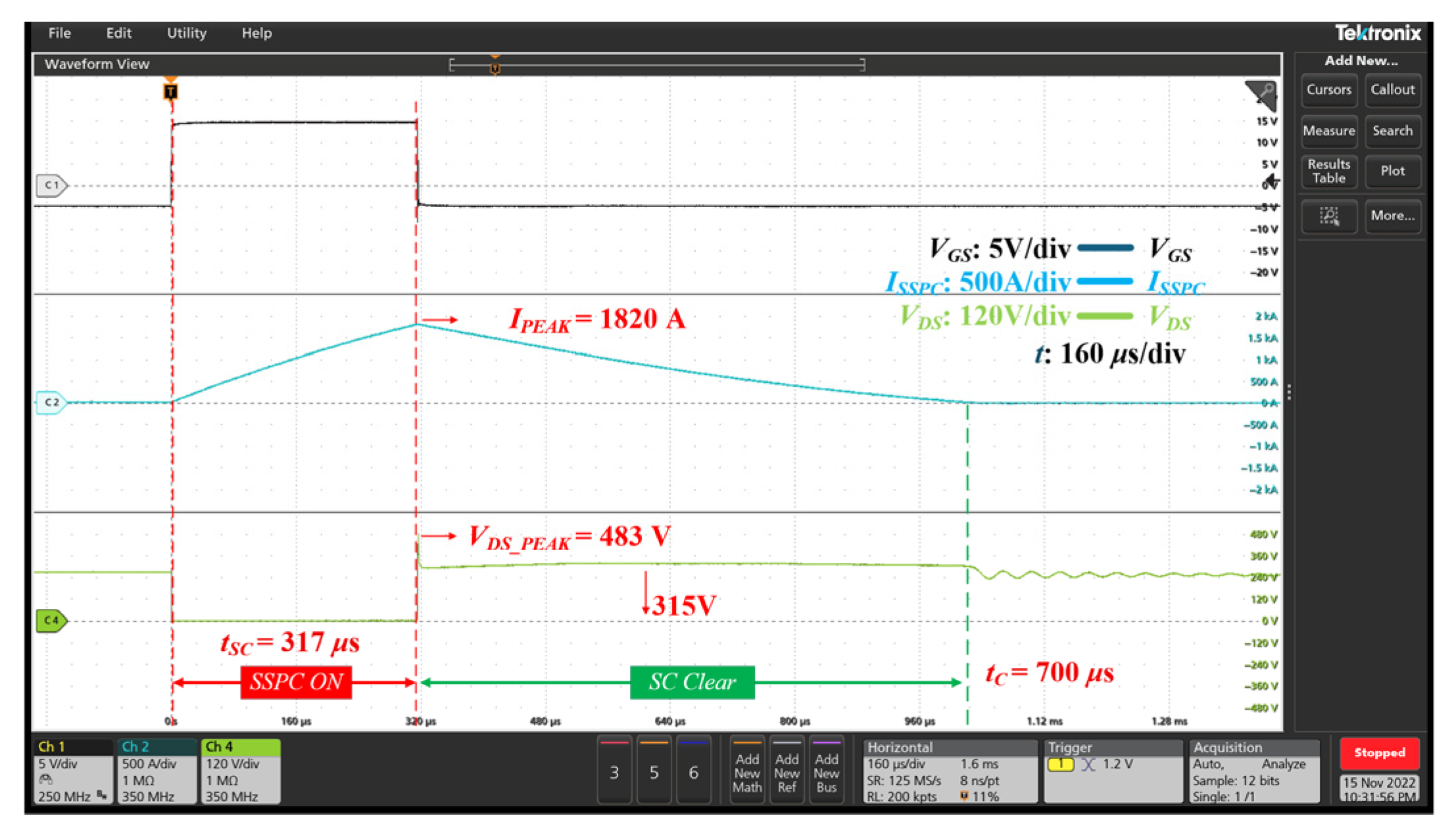
Figure 24 illustrates the turn-off waveform of the SSPC under a short-circuit fault, where the peak short-circuit current reached 1.82 kA. During the short-circuit turn-off process, the drain-source voltage peaked at 483 V, and the total turn-off duration was 700 µs. The results indicate that the proposed SSPC design strategies can successfully balance the current among the 9 branches and effectively mitigate the voltage spike during short-circuit faults.
6.5. Thermal Experiment
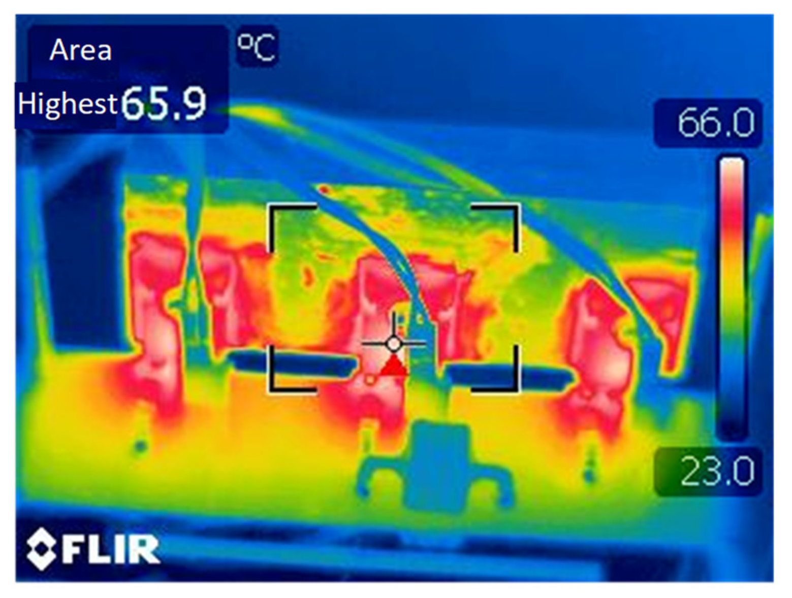
Thermal performance of a single power module was evaluated under the load current of 100 A.
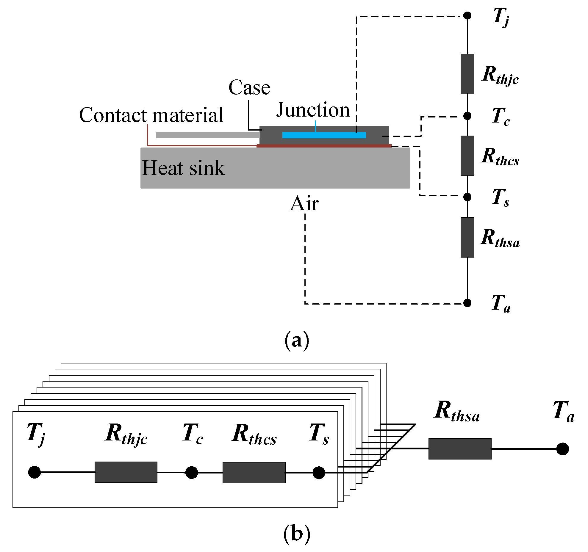
Figure 25 shows the temperature distribution of the module after 30 min of stable operation at an ambient temperature of 23 °C. The maximum measured case temperature of the power device was 65.9 °C, which is in close agreement with the estimated junction temperature of 68 °C, exhibiting a difference of approximately 2.1 °C.
6.6. Applicability and Limitations
The current design establishes a foundational framework for SSPC applications, and its analysis has not been formally verified for compliance with applicable certification standards. To address the specific influences on component selection and system robustness, the following points should be considered for aircraft integration.
Firstly, concerning high-altitude operation and partial discharge, the busbar spacing (e.g., 4 mm used in the prototype) is a preemptive design based on the understanding that creepage and clearance requirements significantly increase with altitude. The final specification must be determined by the maximum altitude of the specific aircraft and relevant environmental standards. Regarding EMC robustness, the TVS is not designed to withstand direct, several-kilovolt ESD or lightning surges. A system-level design, such as installing the SSPC within a well-grounded metallic enclosure, is mandatory to shunt such high-energy transients. Furthermore, for communication robustness in a harsh aircraft electromagnetic environment, the prototype wiring should be enhanced to a 120 Ω shielded twisted pair for the CAN bus, complemented by differential isolation.
These design measures enhance the SSPC compatibility with the stringent requirements of airborne applications.
