Article

Two-Stage Power Delivery Architecture Using Hybrid Converters for Data Centers and Telecommunication Systems

by
Ratul Das
1,* and
Hanh-Phuc Le
2
1
Department of Electrical and Computer Engineering, University of Minnesota Twin Cities, Minneapolis, MN 55455, USA
2
Department of Electrical and Computer Engineering, Jacobs School of Engineering, University of California San Diego, La Jolla, CA 92093, USA
*
Author to whom correspondence should be addressed.
Electronics 2025, 14(16), 3169; https://doi.org/10.3390/electronics14163169
Submission received: 8 July 2025 / Revised: 1 August 2025 / Accepted: 4 August 2025 / Published: 8 August 2025
(This article belongs to the Special Issue Applications, Control and Design of Power Electronics Converters)

Abstract

This paper presents a new power delivery architecture to bring AC distribution voltages to core levels for computing loads using only two conversion stages with new converter topologies to potentially replace the traditional four-stage structure in the development of new data centers. This paper also includes new converters as solutions to the proposed two stages. A new switched capacitor (SC)-based AC-DC converter is proposed for the first stage and demonstrated for an intermediate bus with 90 V–110 VAC to 48–60 VDC conversion and power factor correction. The second stage also includes an SC-based hybrid converter with multi-phase operation suitable for power delivery for core voltages of up to ~1 V with a high current density. This work also reports a new phase sequence for the second stage for an extended output voltage range. Individually, the first stage was measured at 96.1% peak efficiency for output currents ranging from 0 to 4.5 A, while the second stage achieved 90.7% peak efficiency with a load range of 0–220 A at 1V. The measured peak power densities were 73 W/in3 for the first stage and 2020 W/in3 for the second stage. In combination, the direct conversion from ~110 VAC to 1 VDC led to a peak efficiency of 84.1% at 50 A, and this setup has been tested with output currents of up to 160 A, where the efficiency was 73.5%.

1. Introduction

In today’s rapidly evolving technological landscape, a significant number of both industrial and household devices are seamlessly powered by AC power distribution lines, even though an impressive majority inherently function as DC loads. The dominance and rapid proliferation of these DC loads have been nothing short of extraordinary, with their energy demands becoming alarmingly stringent and precise over the years. This scenario is particularly striking in the realm of modern data centers and cutting-edge telecommunication systems. These advanced facilities epitomize the shift, as they heavily depend on high-performance processors that compulsorily require a sophisticated array of power converters to adeptly interface with AC distribution lines [1]. The insatiable appetite for modern data processing capabilities, coupled with escalating computation and storage demands, has propelled these processors into a realm of unprecedented power consumption. Consequently, this surge in power demand manifestly results in an extraordinarily high loading current at critically low supply voltages of ~1 V.
In conventional configurations, high-performance computing rack servers within data centers are supplied with power from an AC grid through an isolation transformer, which is subsequently followed by an online Uninterruptible Power Supply (UPS) and typically involves four stages [1,2]: (1) a power factor correction (PFC) rectifier that transitions the AC line voltage to a high-voltage DC-link bus, (2) the subsequent stage that transforms the DC-link to an intermediate DC bus at a nominal 48 V, (3) a high-efficiency DC-DC conversion from 48 V to 12 V, and (4) the final stage that converts 12 V to core voltages ranging from 0.8 V to 3.3 V. This architecture is depicted in Figure 1a. Generally, isolation is necessitated only at one stage from the grid to the core levels, for which a high-power isolation transformer is deployed either before or after the UPS. Although transformers are frequently employed in AC-DC and DC-DC conversion methodologies due to their dependence on them, the transformers utilized in the last four stages fail to offer the safety-rated isolation required. The sequential connection of multiple stages culminates in an overall diminishment in power efficiency and density, producing an excessive thermal output that necessitates substantial and costly cooling systems. With recent rapid advancements in data management and processing [3,4,5,6], alongside the emergence of 5G communications, artificial intelligence, cryptocurrency, and cloud-reliant data processing and computations, the escalation in power demand is anticipated to be increasingly challenging. Consequently, the conventional multiple power delivery architecture emerges as a significant impediment to system performance and cost-efficiency and should thus be supplanted by more advanced, optimized, and efficient solutions.
Enhancing power delivery and management is pivotal in reducing the expenditure associated with the construction and operation of future green data centers, thereby addressing the rapid expansion of high-performance computing capabilities. In pursuit of this critical objective, the adoption of a minimized number of conversion stages featuring high-conversion-ratio converters presents itself as a particularly viable strategy to streamline the power delivery rack and augment efficiency. Motivated by this standpoint, the present study demonstrates an efficient AC-to-core power delivery architecture for data centers and telecommunication systems, utilizing merely two direct conversion stages: (1) the AC to 48–60 V step-down power factor correction (PFC) rectifier and (2) 48–60 V to 0.8 V–3.3 V DC-DC converter stages. The proposed power delivery architecture is depicted in Figure 1b.
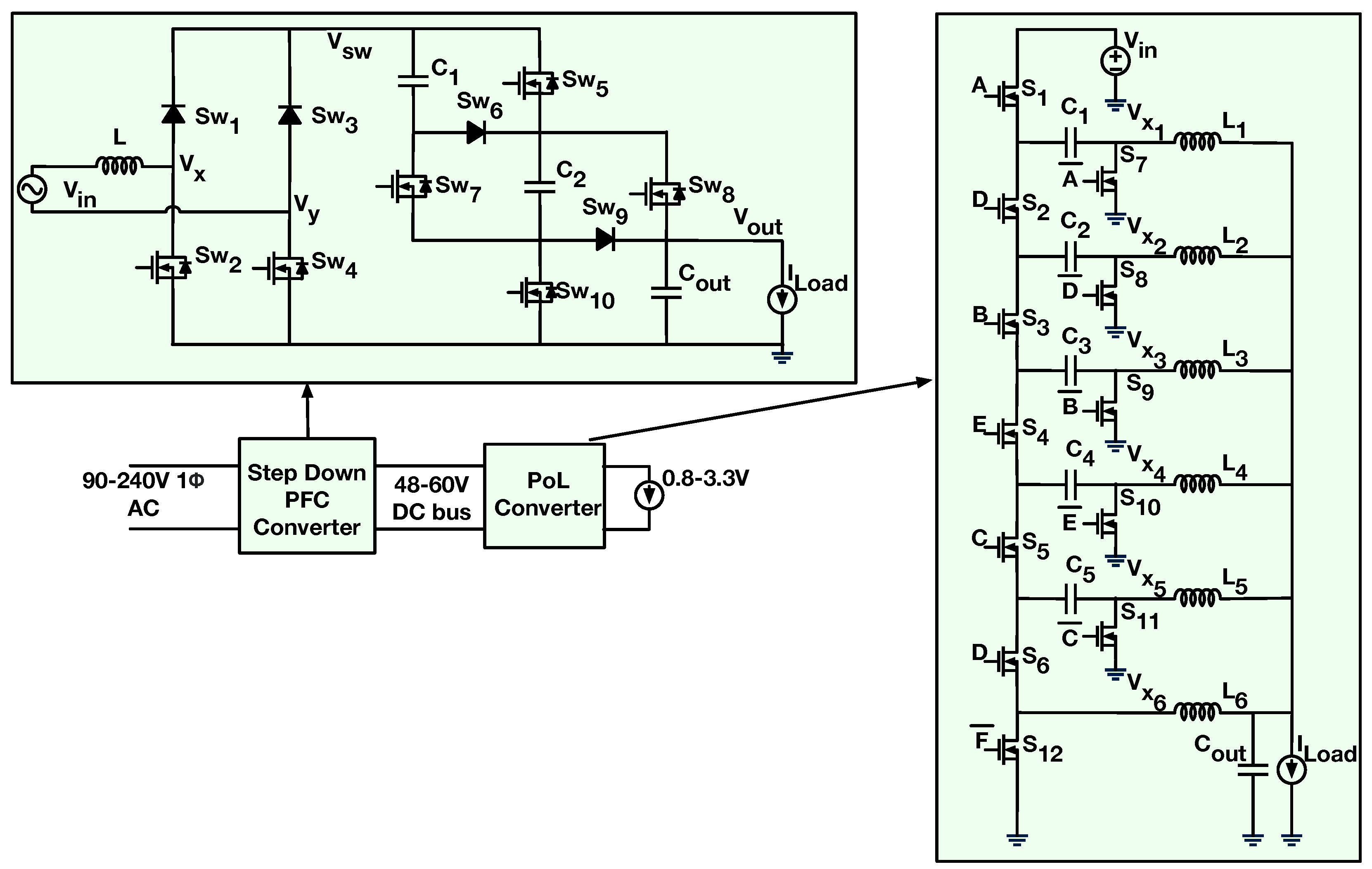
The two converter stages were designed using hybrid converters that strategically combine switched-capacitor and inductor operations to enhance both efficiency and power density. The comprehensive structure, along with device-level details, is depicted in Figure 2. In this study, the PFC rectifier stage features a novel multilevel hybrid converter, which employs partial series–parallel switched-capacitor operations to diminish the inductor value and total harmonic distortion. Additionally, it steps down and shifts the DC link to a lower voltage level, specifically a nominal 48 V, allowing for the use of high-density capacitors for energy buffering. By utilizing rapid input current and slower output voltage control loops, this converter effectively regulates both the output voltage and input current, thereby maintaining favorable power factors and efficiency. The last-centimeter point of load (PoL) converter demonstrated herein is a GaN-based multi-phase, multi-inductor hybrid (MP-MIH) converter, engineered to deliver extremely high output currents at low voltages with an exceptionally high current density. The organization of this paper is as follows: Section 2 and Section 3 provide a detailed discussion on the PFC step-down and MPMIH converters, addressing operation and design considerations. Section 4 presents the experimental results, and the paper is concluded with a summary in Section 5.

2. Step-Down PFC Converter

Traditional AC-DC conversion with moderate to high power generally uses a bridgeless PFC converter [7,8]. There are different control schemes adopted to regulate input current and output voltage to support the basic operation of this converter [9]. While this converter can achieve a very good displacement power factor or near-zero phase lag between the input voltage and current, the distortion power factor can still deteriorate because of switching current ripple at high input voltages. The switching current ripple magnitude can be made smaller with a larger input inductance, higher switching frequency, and/or lower voltage stress. While increasing the inductance requires a larger-sized inductor, which leads to a lower power density, increasing the switching frequency may not be desirable because an optimal value is highly dependent on particular semiconductor devices and the core materials of the inductor. From this consideration, topological modifications that allow for smaller voltage stress on the input inductor and active devices could be a better solution to achieve the design goal.
The modular multilevel converter has become popular for its topological advantages, and it is widely used in DC-AC applications. There are also reports on switched-capacitor architectures for conversion from a single DC voltage to a high-voltage AC output [10,11,12]. However, the converter type has been found to have been much less explored in AC-DC conversion applications. In this work, the architecture of an S-hybrid converter [13] is modified and merged with a bridgeless or totem-pole PFC converter for AC-DC applications. The following section describes the topology and operation of the converter.

2.1. Topology and Operation

As shown in Figure 2, the presented PFC step-down hybrid converter has one current-shaping inductor, L, and four switches, Sw1–4, in the main rectifier. These switches operate at high frequency during the low-voltage fraction of the line cycle, while staying idle, on or off, for the remaining time. A switched-capacitor (SC) circuit follows the rectifier to provide the stepped-down output as well as multilevel switching voltages for the inductor. In this demonstration, the SC circuit has two flying capacitors, C1–2, and six switches, Sw5–10. These switches also operate at the converter’s operating frequency during designated periods of the line cycle.
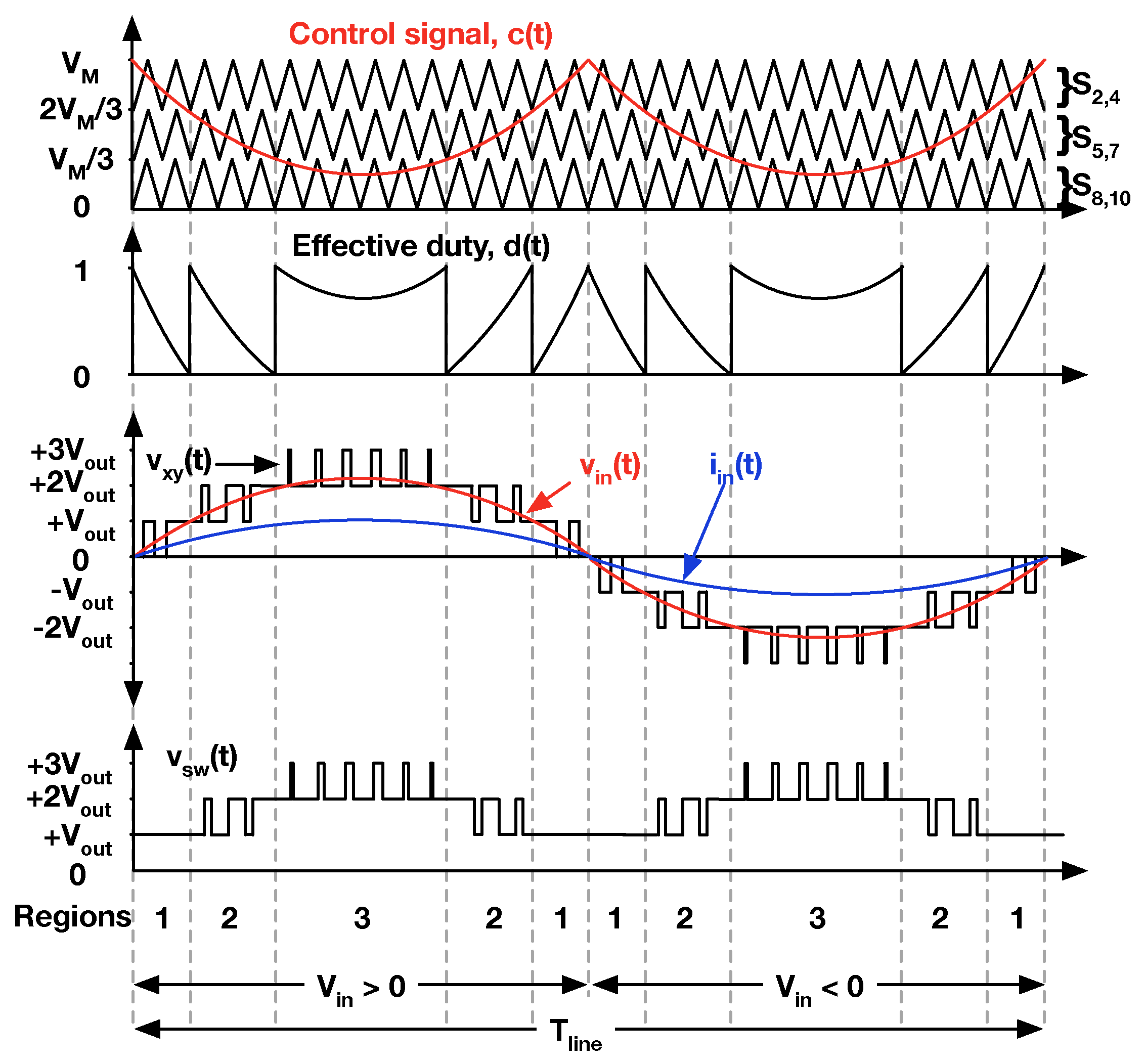
Figure 3 depicts the simplified ideal operational waveforms of the full converter during a full line cycle. All capacitors are expected to have negligible voltage ripples and equal voltages. Consider an input voltage with a peak value of Vm such that 2 Vout ≤ Vm < 3 Vout; the full line cycle can be divided into three time regions: (1) region 1: 0 ≤ |Vin| < Vout; (2) region 2: Vout ≤ |Vin| < 2 Vout; and (3) region 3: 2 Vout≤ |Vin| < 3 Vout. For any of these regions, the converter switches are operated in such a way that Vxy switches in a pulse-width-modulated (PWM) control manner between the upper and lower limits of the region to generate an average voltage equal to Vin. The rectifier switches, Sw1–4, take care of selecting the right polarity of Vxy in accordance with the input voltage being positive or negative. As a result, Vxy switches between seven levels (0, ±Vout, ±2 Vout, and ±3 Vout).
The SC configurations used to generate different switching node Vsw voltages suitable for different input voltage levels are shown in Figure 4. In operation, Sw5,7 are turned on and off together while Sw6 is their complementary switch. In a similar way, Sw9 is the complimentary of Sw8,10. The rectifier switches, Sw1–4, bridge the SC configurations with the input inductor and the source. In this proof-of-concept demonstration, Sw1,3,6,9 are implemented with diodes for simplicity, while Sw1,2,5,7,8,10 are implemented with MOSFETs to control the operation of the converter. The switch selection for the main rectifier was carried out following a standard bridgeless PFC converter design [7].
In order to control the switches, PWM control signals can be acquired by comparing a control signal, c(t), with three separate carrier signals in three different voltage domains, as shown in Figure 3. The control signal can be generated by weighing the regulation information for the output voltage and input current in accordance with required output power and the input voltage. In particular, when c(t) is in the first region, Sw2 is switched at the carrier frequency when Vin > 0, while the switching of Sw4 is activated when Vin < 0. Sw5,7 and Sw8,10 are activated with c(t) in the second and third regions, respectively. In a practical implementation with digital PWM modules in a micro-controller, the effective duty cycle, d(t), can be calculated digitally based on similar information and used to generate the PWM signals. Following reference [13], d(t) can be calculated as
d ( t ) = 1 | V i n | V o u t when , 0 | V i n | < V o u t 2 | V i n | V o u t when , V o u t | V i n | < 2 V o u t 3 | V i n | V o u t when , 2 V o u t | V i n | < 3 V o u t
Utilizing Equation (1) and assuming V M = 1 , a separate set of expressions for d(t) can be derived in terms of c(t), which is useful for directly generating the PWM signals for the switches using different PWM modules in the micro-controller:
d ( t ) = 3 c ( t ) 2 when , 2 3 c ( t ) 3 c ( t ) 1 when , 1 3 c ( t ) < 2 3 3 c ( t ) when , 0 c ( t ) < 1 3
Note that the switches in the SC circuit block 3× times smaller voltages compared to the switches in the main rectifier. Therefore, these switches can be selected with a smaller voltage rating, lower RDS,on, and lower parasitic capacitance to improve overall performance with reduced conduction and switching losses.

2.2. Modified Operation for Capacitor Balancing

In the operation described in Figure 4, flying capacitors C1–2 and the output capacitor Cout are placed either parallel or stacked in series to generate Vout, 2Vout, and 3Vout levels at the switching node, Vsw. To generate 2Vout, C1 can be stacked on top of C2 and Cout (configuration option 1), as shown in Figure 4b, or a parallel combination of C1 and C2 can be placed on top of Cout, as shown in Figure 4c (configuration option 2). Although theoretically capable of supporting the 2Vout needed for operation, using only one of these configurations causes a high capacitor voltage ripple problem for capacitors C1 and C2 in region 3, where Vsw is switched between 2Vout and 3Vout. Particularly, if only configuration option 1 is used, C1 keeps receiving charges without redistribution to lower capacitors as the converter stays in region 3. On the other hand, if only configuration option 2 is used, both C1 and C2 keep receiving charge without redistribution to Cout and the load. The excessive charge for the flying capacitor(s) in region 3 where the input current is at its peak will cause a high voltage ripple, significant hard-charging loss, and risks of over-voltage damages for both capacitors and active switches. In addition, the over-charged voltage in the flying capacitors also causes unwanted variations in the average voltage of Vxy, which in turn distorts the current waveform, increasing current harmonics and reducing the power factor.
The overcharging problem in flying capacitors was identified in [10] for the example of an inverter with a slightly different topology and operation. It was also suggested to make the flying capacitor large enough to keep the over-voltage within a certain range. However, this method becomes less effective in high-power applications, where the input charging current is large or very large capacitors are required. To avoid using an excessive area for more capacitance, in this work, we introduce a relatively simple operational solution to solve this problem.
Recognizing that the key to the solution is charge redistribution among the flying capacitors and to the output capacitor, we combine and alternate both configurations, option 2 (Figure 4c) and option 1 (Figure 4b), in each switching cycle to generate Vsw = 2Vout. In this way, the input charge is redistributed to the load every two switching cycles.
To implement this modified control, simple logic conditions can be added to generate alternative PWM signals from the second and third levels of multilevel carrier signals, as shown in Figure 3, for Sw5,7 and Sw8,10. These conditions can be activated for the full line cycle without changing the basic operation of the converter. Figure 5a depicts the simplified logical diagram for the modified operation.
To generate these control signals with a smooth transition between different regions in a more practical implementation in a micro-controller, carrier signals can be modified as shown in Figure 5b, where the second and third carrier signal levels are implemented with two 180° phase-shifted PWM signals with magnitudes from 0 to 2 V M 3 . In this way, at least once in every two switching periods, C1 is placed in parallel to C2 and C2 is placed in parallel to Cout, which is tightly regulated. This operation makes sure the flying capacitors closely track the regulated output voltage Vout as frequently as every other switching cycle.
It is worth noting that this over-voltage problem does not come into the scene in regions 1 and 2 as charge redistribution to Cout and Vout happens once in every switching period, keeping an equal voltage for all the capacitors, V C 1 = V C 2 = V C o u t = V o u t . Also, the increased voltage for C1 in this converter is different than the imbalance problem in FCML converters. The resultant voltage variation in this converter occurs at the line frequency, does not depend on small timing mismatches [14], and can be calculated quite precisely with existing models.

2.3. Advantage of the Proposed Converter: Reduced Inductor Current Ripple

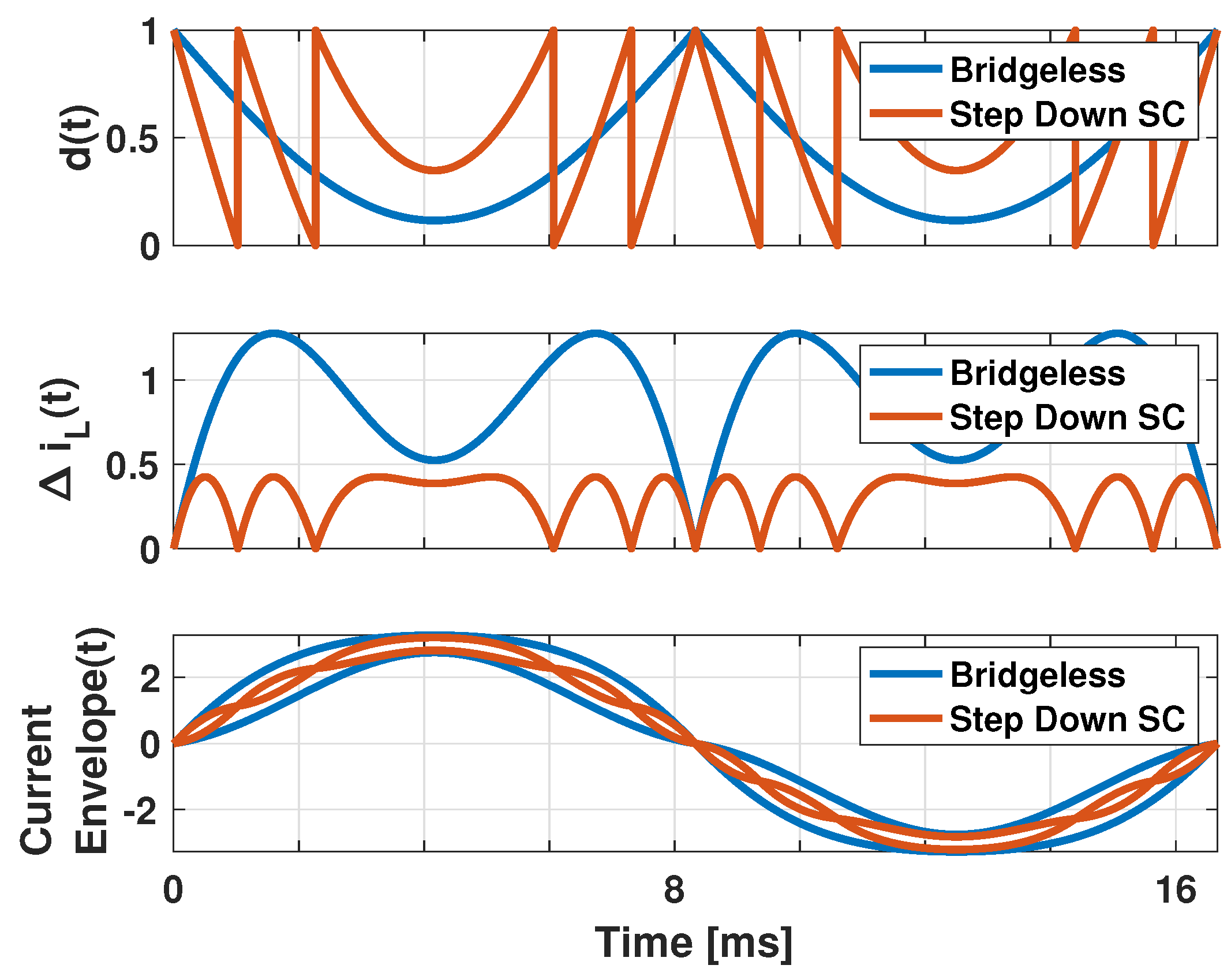
With two flying capacitors and an output capacitor, this converter can generate seven levels for the Vxy node voltage. As a result, in a major portion of the line cycle, the inductor is charged and discharged by a smaller amount of voltage compared to a bridgeless or totem-pole PFC converter. In particular, in region 1, the inductor is switched to either input voltage or Vout, which is smaller than Vm. In region 2, the inductor voltages are |Vin| − Vout and 2 Vout − |Vin|, while in region 3, they are |Vin| − 2 Vout and 3 Vout − |Vin|. Using the inductor voltage information, the current ripple of the step-down PFC converter is calculated and compared with a bridgeless/totem-pole PFC converter at the same power and operating point, as shown in Figure 6. It can be observed that the new step-down PFC converter maintains smaller current ripples and thus a narrower envelope of the inductor current throughout the operation. Hence, one can also predict a superior THD performance in the new converter compared with a bridgeless/totem-pole PFC converter under the same operating conditions.

2.4. Advantage of the Proposed PFC Converter: DC-Link Filtering with Distributed Low-Voltage Capacitors

In any AC-DC or DC-AC application, the choice of total DC-link capacitance depends on the line frequency, maximum power, and maximum allowed voltage ripple. The amount of capacitance is typically very large considering the large output power and low line frequency. The presented step-down PFC converter also falls into this general category. However, as opposed to conventional PFC converters, this converter carries out the DC-link filtering function at low-output voltage levels. More importantly, the switched-capacitor operation with efficient charge redistribution, as described in Section 2.2, allows all flying capacitors and the output capacitor to participate as DC-Link capacitors. A key benefit here is that this allows the large DC-Link capacitance to be distributed among the flying capacitors with no difference in energy buffering performance. As an additional benefit, the large values of flying capacitors minimize their switching-frequency ripple and hard-charging loss to improve overall efficiency. The low output voltage rating requirement also enables the selection of higher-density capacitors to reduce overall implementation size and increase the system’s power density.
As a design aspect, one needs to choose between electrolytic and ceramic capacitors for the converter. The design can be made electrolytic-free by using ceramic capacitors either with or without methods to enhance the energy buffering capability of the capacitors, for example, using a series stacked energy buffer [15] or stacked switched-capacitor buffer [16]. While there are certain benefits to an electrolytic-free implementation, the main drawback associated with using only ceramic capacitors for both flying and output capacitors is that they are more expensive and have relatively lower energy density compared with electrolytic capacitors.

2.5. Control and Sensing Circuits

The traditional feed-forward average-current-mode control for a PFC boost converter was employed to control this new converter [9]. Figure 7 illustrates a block diagram of the control procedure in a micro-controller. While the controller ground was chosen as the negative terminal of the converter’s output, it simplified the sensing of the output voltage. For input voltage sensing, a simple rectifier followed by a resistive divider was chosen to provide the required input voltage to the controller through an analog-to-digital conversion. A Hall effect sensor was used for current sensing purposes.
The small-signal model analysis of the converter’s input current response and output voltage indicates that the converter behaves the same way as multilevel converters and standard PFC boost converters [17]. Thus, long-existing and well-adopted knowledge for the control of a PFC boost converter can readily be used to design the voltage compensator, Gcv, and current compensator, Gci. Detailed steps for this design can also be found in [9] and thus have not been included here. Delay-associated poles from the micro-controller were also considered to properly design the compensators [18].

3. Multi-Phase, Multi-Inductor Hybrid Converter

Recently, the last-stage converter for 48 V to 1 V conversion has received a lot of interest in industry and academic research, with remarkable implementations using both isolated [19,20] and non-isolated architectures [21]. In this work, we utilize a member of the multi-inductor hybrid (MIH) converter family [22,23], a six-level converter extension of the previously demonstrated DP-MIH converter reported in [23]. The additional inductors and interleaved phases are extended to support larger output currents compared to prior works.

Multi-Inductor Converter with Multi-Phase Operation

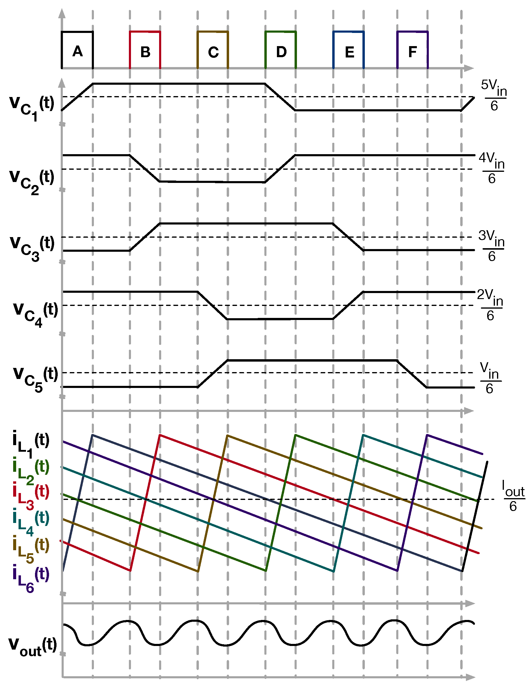
The six-level MP-MIH converter is depicted in Figure 2. It has twelve switches, S 1 12 , five flying capacitors, C 1 5 , and six inductors, L 1 6 . The input switched-capacitor (SC) network divides the input voltages by 6 to feed them into Buck-like output filter inductors, which, in turn, synchronously soft-charge and soft-discharge the flying capacitors. The six high-side switches, S 1 6 , are controlled by six multi-phase, pulse-width-modulated (PWM) signals, A–F, with duty cycle D, while the ground-connected, freewheeling switches, S 7 12 , are controlled by six complementary signals, A ¯ F ¯ , respectively. Accordingly, the output voltage and flying capacitor, C i , voltages can be represented by V o u t = D V i n 6 and V C i = 6 i 6 V i n , where i = 1 5 . The key constraint in the converter operation is that no two consecutive signals controlling two consecutive high-side switches in S 1 6 can overlap. Following this constraint, the converter can support an operation of two to six interleaving phases with the six inductors of the six-level converter. While the maximum number of phases yields advantages in output voltage ripple and transient response, as well as switching loss reduction, it also limits the maximum duty cycle and thus the maximum output voltage. For example, six phases are non-overlapping and evenly distributed with a 60° phase shift, and A–F are arranged for the switches Sw1–6 sequentially; each of the phases A–E has a maximum duty cycle of 1 6 , limiting the maximum output voltage to V i n 36 . However, it is also possible to arrange the phases in a different, non-sequential way to allow for a larger maximum duty cycle while still satisfying the requirement of no overlap between consecutive phases. Figure 8 depicts an example operation, where steady-state operation of an MP-MIH converter is carried out using this strategy. The six non-overlapping phases, in the order of A to F, are limited to 3 6 , 2 6 , 2 6 , 3 6 , 3 6 , and 3 6 , respectively. This arrangement allows for a maximum output voltage, V i n 18 , while still obtaining the benefits of a six-phase interleaving operation with equal duty cycles. When a maximum output voltage is prioritized, the converter operation can be changed to two-phase interleaving to reach an output voltage of V i n 12 .

4. Experimental Results

The two-stage 110 VAC-to-1 VDC power delivery architecture was implemented using two converter prototypes, as shown in Figure 9a,b. The key components for the converters are listed in Table 1 and Table 2. These converters were tested separately and in combination to demonstrate the full structure.

4.1. Step-Down PFC Converter

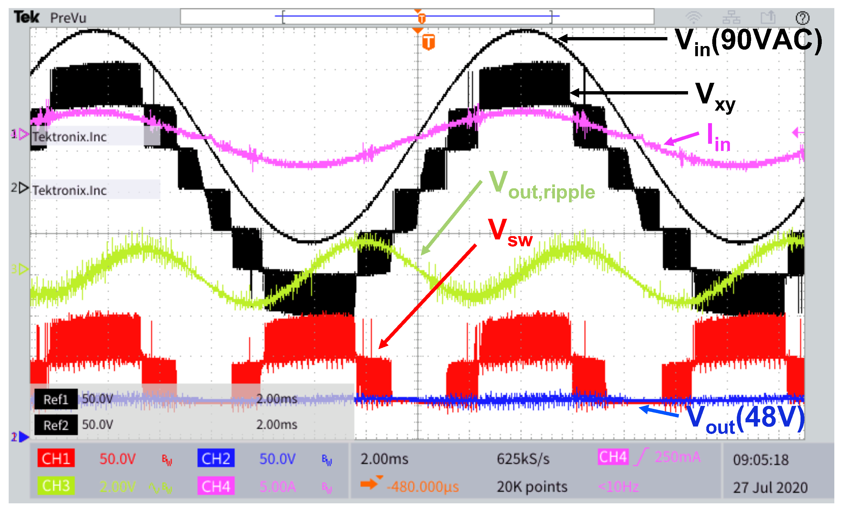
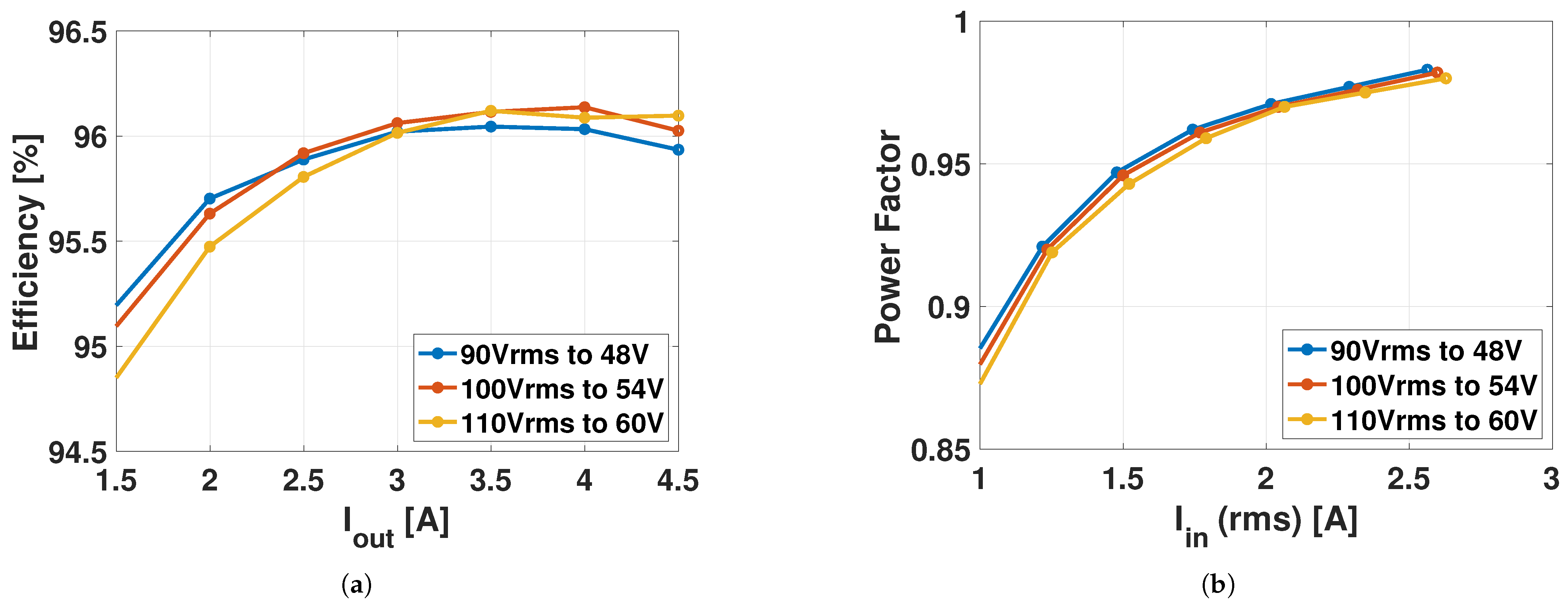
Figure 10 shows the key waveforms of the converter during 90 VAC to 48 V/4 A operation. It can be seen that the input current follows the input voltage, verifying the key PFC operation. The performance of the converter is shown in Figure 11 in terms of efficiency and the power factor. The converter maintains an efficiency of higher than 96% for a wide range of operations and more than 95% for almost all operating points. As shown in Figure 11b, the converter achieves a power factor of 0.98 at a 2.6 A effective input current. The power factor goes down at a lower input current, i.e., a lower output power, because of the noise and harmonics caused by multilevel switching operations that couple to and reduce the accuracy of the current sensor and the current regulation loop. The power density of this converter at the full power is 73 W/in3, including all the components, including output electrolytic capacitors.

4.2. MP-MIH Converter

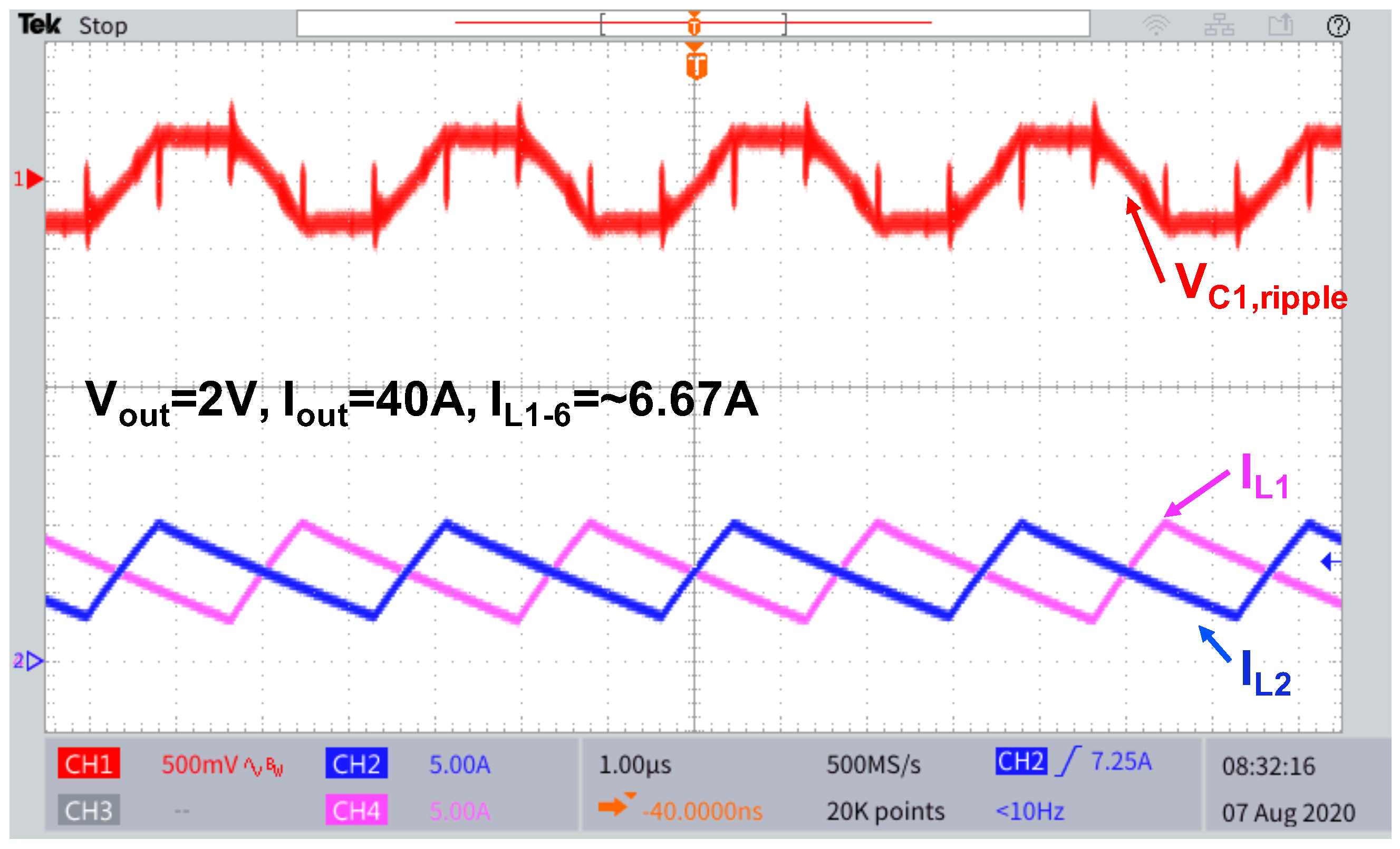
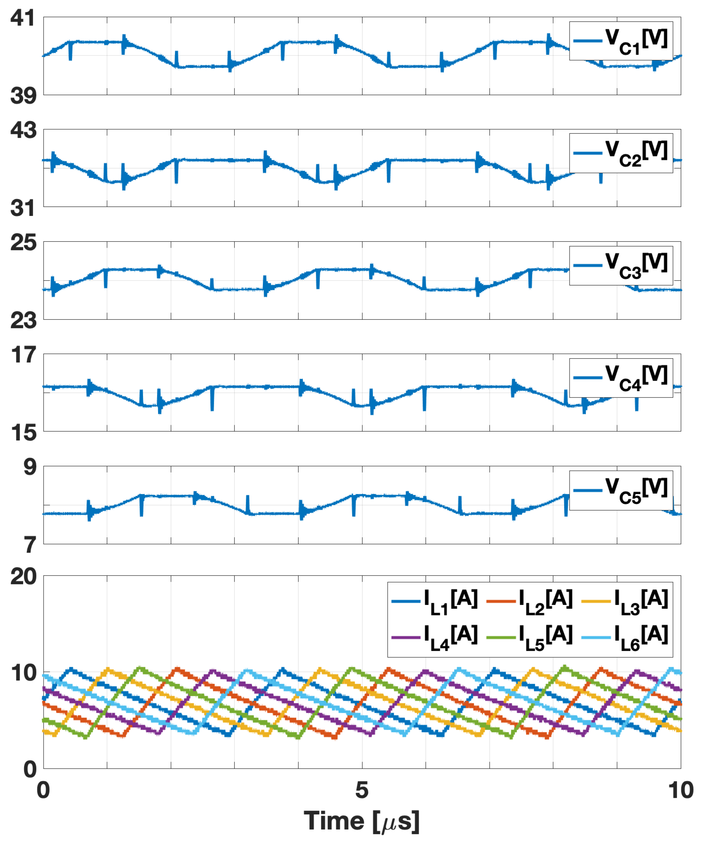
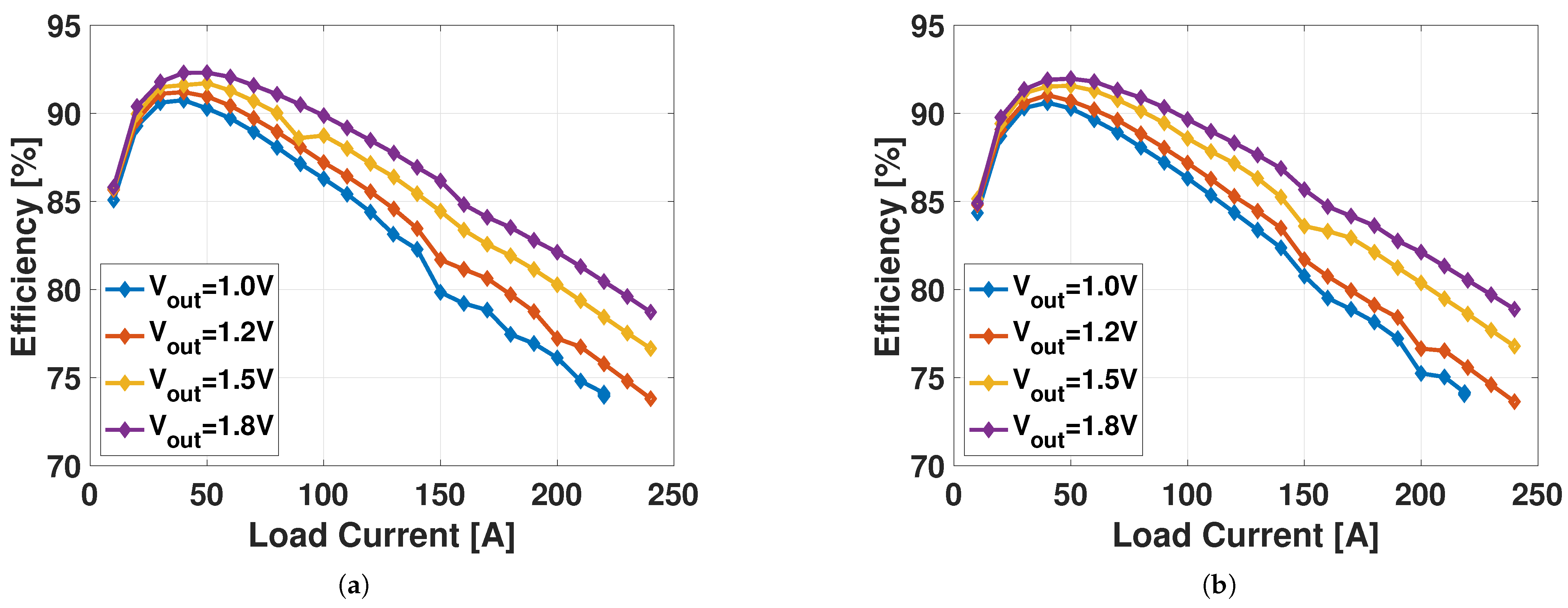
Figure 12 and Figure 13 show the key waveforms of the MPMIH converter in a 48 V to 2 V/40 A operation example. In accordance with the phase sequence selection presented in Figure 8, the converter’s output current was a six-phase interleaved combination of inductor currents. The standalone performance of this converter is presented in Figure 14. During 48 V to 1 V operation, this converter achieved a peak efficiency of 90.75% at a 40 A load current, whereas 92.31% efficiency was achieved for a 48 V to 1.8 V conversion and at a 50 A output current. The converter was tested up to a maximum load current of 220 A at 1 V and 240 A at 1.2–1.8 V. Considering the components in the power flow path, this converter achieved a current density of 1.03 kA/in3 for 1 V and 1.123 kA/in3 for the other output voltages, which translates to 1.03 kW/in3 and 2.02 kW/in3 peak power densities for 1 V and 1.8 V output voltages, respectively. Similar experiments have also been carried out for a 54 V input voltage. At a 54 V input voltage, this converter achieved peak efficiencies of 90.6% and 92% for 1 V and 1.8 V output voltages, respectively.

4.3. Full System Verification

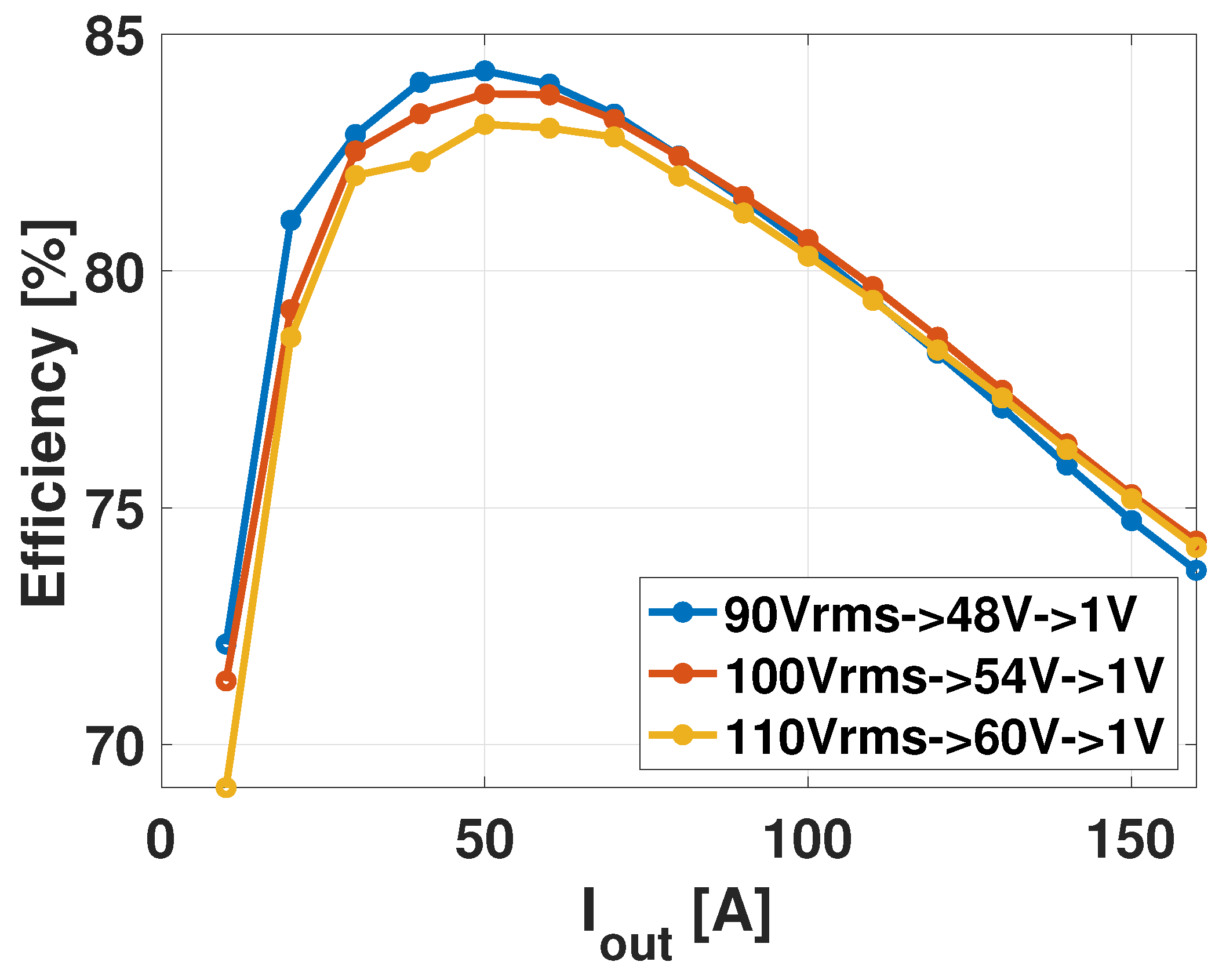
The MP-MIH converter was connected to the step-down PFC converter’s output to complete the full power delivery system that bridges the gap between an AC distribution voltage and core DC voltages. Figure 15 shows the operations of the full system in line and load transients. The waveforms of the input inductor current ( I i n ), output current ( I o u t 4 ), switching voltage ( V s w ), and output voltage ( V o u t ) illustrate stable operations and regulations of the converter and output voltage when the converter is exposed to a 40 Vrms line voltage step (Figure 15a) and a 50 A load step (Figure 15b). The first-stage step-down PFC hybrid converter can provide a fast response to large line transients thanks to the flying capacitors, which are capable of changing between multiple levels, while remaining variations at the output of the first stage are managed by the second-stage regulations. The seamless duty cycle control from the second stage also takes care of the high load current transient at the final output. The overall efficiency of the system is shown in Figure 16. For 110 VAC-to-1 VDC operation, the overall peak efficiency is 84.1%. The peak output current when testing the full system is limited to 160 A because of a non-fundamental limit in the design of the first-stage AC-DC converter, which has an output current of less than 4.5 A.
For comparison, a conventional power delivery architecture using four conversion stages for the same application would require all stages to individually achieve, on average, an efficiency of 95.8% to reach an equivalent performance to this proposed two-stage architecture. Considering the full conversion from 110 VAC to 1 VDC, to the authors’ best knowledge, this has not been demonstrated.

5. Conclusions

In this work, we successfully demonstrated the first two-stage architecture that is able to directly convert an AC distribution voltage to core voltages, which could be used for power delivery in data centers and telecommunication systems. The demonstration includes a new switched-capacitor, multilevel, step-down PFC converter and a six-level, switched-capacitor-based, multi-phase, multi-inductor hybrid (MPMIH) converter. The operation of the step-down PFC converter was discussed with control mechanisms for output voltage and input current regulations. A simple method of charge redistribution for flying capacitor voltage balancing at the carrier switching frequency was also provided. In designing the MP-MIH converter, a new phase sequence was proposed and verified through experiments for larger output voltage and current ranges. The converter designs were verified separately and together in the complete two-stage AC grid-to-core voltage system, demonstrating promise for future applications to contribute to greener and more energy-efficient data centers, telecommunication, and other IT systems.

Author Contributions

Conceptualization, R.D. and H.-P.L.; methodology, R.D.; software, R.D.; validation, R.D.; formal analysis, R.D.; investigation, R.D.; resources, R.D. and H.-P.L.; data curation, R.D.; writing—original draft preparation, R.D.; writing—review and editing, H.-P.L.; visualization, R.D.; supervision, H.-P.L.; project administration, H.-P.L.; funding acquisition, H.-P.L. All authors have read and agreed to the published version of the manuscript.

Funding

This work was supported in part by the NSF ECCS program award No. 2043025 (previously No. 1810470) and the NSF ECCS CAREER award No. 2042525.

Data Availability Statement

Dataset available on request from the authors.

Conflicts of Interest

The authors declare no conflicts of interest.

References

  1. Pratt, A.; Kumar, P.; Bross, K.; Aldridge, T. Powering Compute Platforms in High Efficiency Data Centers; Technical Report; Intel Corporation: Santa Clara, CA, USA, 2006. [Google Scholar]
  2. Yeaman, P. Datacenter Power Delivery Architectures: Efficiency and Annual Operating Costs; Technical Report; Vicor Corporation: Andover, MA, USA, 2007. [Google Scholar]
  3. Cisco and/or Its Affiliates. Cisco Global Cloud Index: Forecast and Methodology, 2015–2020; Technical Report; 2016; Available online: https://www.cisco.com/c/dam/m/en_us/service-provider/ciscoknowledgenetwork/files/622_11_15-16-Cisco_GCI_CKN_2015-2020_AMER_EMEAR_NOV2016.pdf (accessed on 7 July 2025).
  4. Carson, S.; Lundvall, A. Ericsson Mobility Report June 2022; Technical Report; Ericsson: Stockholm, Sweden, 2022. [Google Scholar]
  5. Krein, P.T. Data center challenges and their power electronics. CPSS Trans. Power Electron. Appl. 2017, 1, 39–46. [Google Scholar] [CrossRef]
  6. Masanet, E.; Shehabi, A.; Lei, N.; Smith, S.; Koomey, J. Recalibrating global data center energy-use estimates. Science 2020, 6481, 984–986. [Google Scholar] [CrossRef] [PubMed]
  7. Mitchell, D.M. AC-DC Converter Having an Improved Power Factor. U.S. Patent US4412277A, 25 October 1983. [Google Scholar]
  8. Chellappan, S. A Comparative Analysis of Topologies for a Bridgeless-Boost PFC Circuit. Tex. Instrum. Inc. Analog. Des. J. 2018, 3, 1–4. [Google Scholar]
  9. Erickson, R.W.; Maksimović, D. Pulse-Width Modulated Rectifiers. In Fundamentals of Power Electronics; Springer International Publishing: Boston, MA, USA, 2020; pp. 867–930. [Google Scholar]
  10. Hinago, Y.; Koizumi, H. A Switched-Capacitor Inverter Using Series/Parallel Conversion with Inductive Load. IEEE Trans. Ind. Electron. 2012, 59, 878–887. [Google Scholar] [CrossRef]
  11. Khan, M.N.H.; Forouzesh, M.; Siwakoti, Y.P.; Li, L.; Blaabjerg, F. Switched Capacitor Integrated (2n + 1)-Level Step-Up Single-Phase Inverter. IEEE Trans. Power Electron. 2020, 35, 8248–8260. [Google Scholar] [CrossRef]
  12. Barzegarkhoo, R.; Siwakoti, Y.P.; Blaabjerg, F. A New Switched-Capacitor Five-Level Inverter Suitable for Transformerless Grid-Connected Applications. IEEE Trans. Power Electron. 2020, 35, 8140–8153. [Google Scholar] [CrossRef]
  13. Seo, G.S.; Le, H.P. S-Hybrid Step-Down DC–DC Converter—Analysis of Operation and Design Considerations. IEEE Trans. Ind. Electron. 2020, 67, 265–275. [Google Scholar] [CrossRef]
  14. Das, R.; Celikovic, J.; Abedinpour, S.; Mercer, M.; Maksimovic, D.; Le, H.P. Demystifying Capacitor Voltages and Inductor Currents in Hybrid Converters. In Proceedings of the 2019 20th Workshop on Control and Modeling for Power Electronics (COMPEL), Toronto, ON, Canada, 17–20 June 2019; pp. 1–8. [Google Scholar]
  15. Qin, S.; Lei, Y.; Barth, C.; Liu, W.C.; Pilawa-Podgurski, R.C.N. A High Power Density Series-Stacked Energy Buffer for Power Pulsation Decoupling in Single-Phase Converters. IEEE Trans. Power Electron. 2017, 32, 4905–4924. [Google Scholar] [CrossRef]
  16. Pervaiz, S.; Kumar, A.; Afridi, K.K. A Compact Electrolytic-Free Two-Stage Universal Input Offline LED Driver With Volume-Optimized SSC Energy Buffer. IEEE J. Emerg. Sel. Top. Power Electron. 2018, 6, 1116–1130. [Google Scholar] [CrossRef]
  17. Erickson, R.W.; Maksimović, D. Current-Programmed Control. In Fundamentals of Power Electronics; Springer International Publishing: Boston, MA, USA, 2020; pp. 725–804. [Google Scholar]
  18. Corradini, L.; Maksimović, D.; Mattavelli, P.; Zane, R. Digital Control of High-Frequency Switched-Mode Power Converters: Corradini/Digital Control of High-Frequency Switched-Mode Power Converters; John Wiley & Sons, Inc.: Hoboken, NJ, USA, 2015. [Google Scholar]
  19. Khatua, S.; Kastha, D.; Kapat, S. A New Single-Stage 48-V-Input VRM Topology Using an Isolated Stacked Half-Bridge Converter. IEEE Trans. Power Electron. 2020, 35, 11976–11987. [Google Scholar] [CrossRef]
  20. Kumar, A.; Pervaiz, S.; Afridi, K.K. High-Performance Single-Stage Isolated 48V-to-1.8V Point-of-Load Converter Utilizing Impedance Control Network and Distributed Transformer. In Proceedings of the 2018 IEEE Energy Conversion Congress and Exposition (ECCE), Portland, OR, USA, 23–27 September 2018; pp. 3838–3843. [Google Scholar]
  21. Ahmed, M.H.; Fei, C.; Lee, F.C.; Li, Q. 48-V Voltage Regulator Module With PCB Winding Matrix Transformer for Future Data Centers. IEEE Trans. Ind. Electron. 2017, 64, 9302–9310. [Google Scholar] [CrossRef]
  22. Abe, K.; Nishijima, K.; Harada, K.; Nakano, T.; Nabeshima, T.; Sato, T. A Novel Three-Phase Buck Converter with Bootstrap Driver Circuit. In Proceedings of the 2007 IEEE Power Electronics Specialists Conference, Orlando, FL, USA, 17–21 June 2007; pp. 1864–1871. [Google Scholar]
  23. Das, R.; Le, H.P. A Regulated 48V-to-1V/100A 90.9%-Efficient Hybrid Converter for POL Applications in Data Centers and Telecommunication Systems. In Proceedings of the 2019 IEEE Applied Power Electronics Conference and Exposition (APEC), Anaheim, CA, USA, 17–21 March 2019; pp. 1997–2001. [Google Scholar]
Figure 1. Traditional and proposed power delivery architecture. (a) Traditional power delivery architecture; (b) proposed power delivery architecture.
Electronics 14 03169 g001
Figure 2. New power delivery architecture with stages implemented using new SC-based hybrid converters.
Electronics 14 03169 g002
Figure 3. Ideal operational waveforms.
Electronics 14 03169 g003
Figure 4. SC configurations to generate different switching node voltages. (a) Vsw = Vout; (b) Vsw = 2 Vout (Option 1); (c) Vsw = 2 Vout (Option 2); (d) Vsw = 3 Vout.
Electronics 14 03169 g004
Figure 5. Modified operation. (a) Logical flow of the modified operation; (b) practical implementation of the modified operation.
Electronics 14 03169 g005
Figure 6. Comparison of current ripples of the step-down PFC converter (90 Vrms to 48 V/4 A) and bridgeless PFC converter (90 Vrms to 3 × 48 V/ 4 3 A) for operation with the same output power, with a 47 µH inductor and 600 kHz switching frequency.
Electronics 14 03169 g006
Figure 7. Controller with sensing circuits.
Electronics 14 03169 g007
Figure 8. Six-level multi-phase, multi-inductor (MP-MIH) hybrid converter and its operation with an AD-BE-CF phase sequence.
Electronics 14 03169 g008
Figure 9. Two converter prototypes of the 110VAC-to-1VDC power delivery architecture. (a) Step-down PFC multi-level AC-DC converter; (b) 6-level MP-MIH DC-DC converter using GaN FETs.
Electronics 14 03169 g009
Figure 10. Steady-state waveforms during 90 Vrms to 48 V/4 A operation of the step-down PFC converter.
Electronics 14 03169 g010
Figure 11. Performance of the step-down PFC converter. (a) Efficiency; (b) power factor.
Electronics 14 03169 g011
Figure 12. Experimental waveforms of I L 1 , I L 2 , and V C 1 in MPMIH converter [during 48 V to 2 V/40 A conversion at 300 kHz with AD-BE-CF phase sequence].
Electronics 14 03169 g012
Figure 13. Measured capacitor and inductor waveforms of the MP-MIH converter prototype for 48 V to 2 V/40 A operation.
Electronics 14 03169 g013
Figure 14. Efficiency of the MP-MIH converter. (a) V i n = 48 V; (b) V i n = 54 V.
Electronics 14 03169 g014
Figure 15. Measured waveforms of the complete two-stage architecture for line and load transients. (a) Operation at 1 V/50 A for a 50 Vrms to 90 Vrms line transient; (b) operation at 1 V from a 90 Vrms input voltage for a 50 A to 100 A load transient.
Electronics 14 03169 g015
Figure 16. Efficiency of the full AC grid-to-core voltage system.
Electronics 14 03169 g016
Table 1. Components used in a PFC step-down converter.
ComponentsPart Number
Sw1,3SBR10U200P5DICT-ND
Sw2,4BSC500N20NS3GATMA1CT-ND
Sw5,7,8,10BSC123N08NS3GATMA1
Sw6,9SBRT20M80SP5-13
C1,28xC5750X7S2A156M250KB
Cout8xC5750X7S2A156M250KB+
4xEKYB101ELL102MM40S
LIHLP6767GZER470M11
Gate driverUCC5350MCDR
Current SensorACS716KLATR-6BB-NL-T
Frequency600 kHz
Table 2. Components used in MPMIH converter.
ComponentsPart Number
Sw1–62xEPC2015c
Sw7–122xEPC2023
C1–54xCGA8M3X7S2A335M200KB
L1–6XAL1030-561ME
Gate DriverLMG1210
Frequency300 kHz
Disclaimer/Publisher’s Note: The statements, opinions and data contained in all publications are solely those of the individual author(s) and contributor(s) and not of MDPI and/or the editor(s). MDPI and/or the editor(s) disclaim responsibility for any injury to people or property resulting from any ideas, methods, instructions or products referred to in the content.