Article

The Role of Modulation Techniques on Power Device Thermal Performance in Two-Level VSI Converters

by
Abraham M. Alcaide
1,2,*,
Jose I. Leon
1,2,
Christian A. Rojas
3,4,
Jhonattan G. Berger
5,
Alejandro Stowhas-Villa
3,
Alan H. Wilson-Veas
6,
Giampaolo Buticchi
7 and
Samir Kouro
3,4
1
Electronic Engineering Department, Universidad de Sevilla, 41092 Seville, Spain
2
ENGREEN Laboratory of Engineering for Energy and Environmental Sustainability, Universidad de Sevilla, 41092 Seville, Spain
3
Electronics Department, Universidad Tecnica Federico Santa Maria, Valparaiso 2390103, Chile
4
Advanced Center of Electrical and Electronic Engineering, Universidad Tecnica Federico Santa Maria, Valparaiso 2390103, Chile
5
Laboratory for Mechatronics and Renewable Energy Systems (LMRES), HM Munich University of Applied Sciences, 80335 Munich, Germany
6
Energy Transformation Center, Engineering Faculty, Universidad Andres Bello, Santiago 7500971, Chile
7
Zhejiang Key Laboratory for More Electric Aircraft Technologies, University of Nottingham Ningbo China, Ningbo 315104, China
*
Author to whom correspondence should be addressed.
Electronics 2025, 14(15), 2934; https://doi.org/10.3390/electronics14152934
Submission received: 2 June 2025 / Revised: 15 July 2025 / Accepted: 18 July 2025 / Published: 23 July 2025
(This article belongs to the Special Issue Applications, Control and Design of Power Electronics Converters)

Abstract

The failure of power semiconductors due to variations in junction temperature represents an important factor in determining the reliability of a power converter. This work presents a comparative assessment of the thermal performance of IGBT power semiconductors within a two-level voltage source converter, specifically the average junction temperature and the variation of this value over a given period. The evaluation was carried out using different continuous and discontinuous carrier-based pulse width modulation (CB-PWM) techniques. The use of discontinuous PWM allows for a decrease in switching losses and therefore in average junction temperatures, but the variation in junction temperature is largely and non-linearly dependent on several factors, including the power factor of the three-phase load. Among the discontinuous PWM techniques, this analysis focuses on those that allow for a symmetric thermal load. The aforementioned comparisons have been tested in a laboratory setup, whee we directly measured the junction temperature through a high-end infrared thermal camera.

1. Introduction

With the increasing demand for efficient and reliable power electronics systems, it is becoming more relevant to address the issue of the aging of power devices [1,2,3,4]. The degradation of power devices can cause system failures, which present important safety concerns and also have significant economic consequences. Therefore, understanding the mechanisms of aging and developing or selecting the most appropriate operating strategy to mitigate the aging of power devices is crucial for the reliable operation of power electronics systems [5,6,7,8].
Although the literature offers multiple options for building a power converter [9], the conventional IGBT-based two-level voltage source inverter (2L-VSI) is still the preferred option in many industrial applications [10]. In a 2L-VSI converter, as shown in Figure 1, the modulation technique determines the switching frequency and the switching patterns of the power devices [10]. The aging of power devices (and therefore, the reliability of the power converter) is affected not only by temperature created by power losses but also by the frequency and pattern of switching, which affect the thermal and electrical stresses on the power devices [11]. Thus, the modulation technique used in the power converter also contributes to the aging of the power devices [12,13]. Among all the modulation techniques provided in the technical literature, the carrier-based sinusoidal pulse width modulation (CB-PWM) family is very popular in industrial applications because of its simplicity, its easy implementation in most microcontrollers and FPGAs, and its good performance.
The aging of power devices is a complex phenomenon that depends on various factors such as operating temperature, current stress, and voltage stress [14,15]. These factors can cause physical degradation in power devices. The aging of power devices can lead to various types of failure, such as short circuits, open circuits, and performance degradation [16,17]. The stress phenomenon in power devices is caused by thermal fluctuations because the materials comprising the power device have different thermal characteristics. These thermal changes cause expansion and contraction of the materials, leading to failure due to solder cracks and lifting of the bonding wires.
In this work, the influence of the selected modulation technique on the mechanisms of aging of power devices in a conventional 2L-VSI is investigated. The aim is to present the most effective technique in terms of the thermal behavior of the power semiconductor according to several aspects such as nominal power, power factor operating point, and switching frequency, among others.
This paper is organized as follows. Section 2 provides an overview of the mechanisms of aging of power devices and the factors that contribute to it. Section 3 presents the modulation techniques studied in this paper, and Section 4 presents their impact on the thermal behavior of power devices. Section 5 presents the experimental setup and the results obtained. Finally, Section 6 concludes this paper with a summary of the main findings and directions for future research.

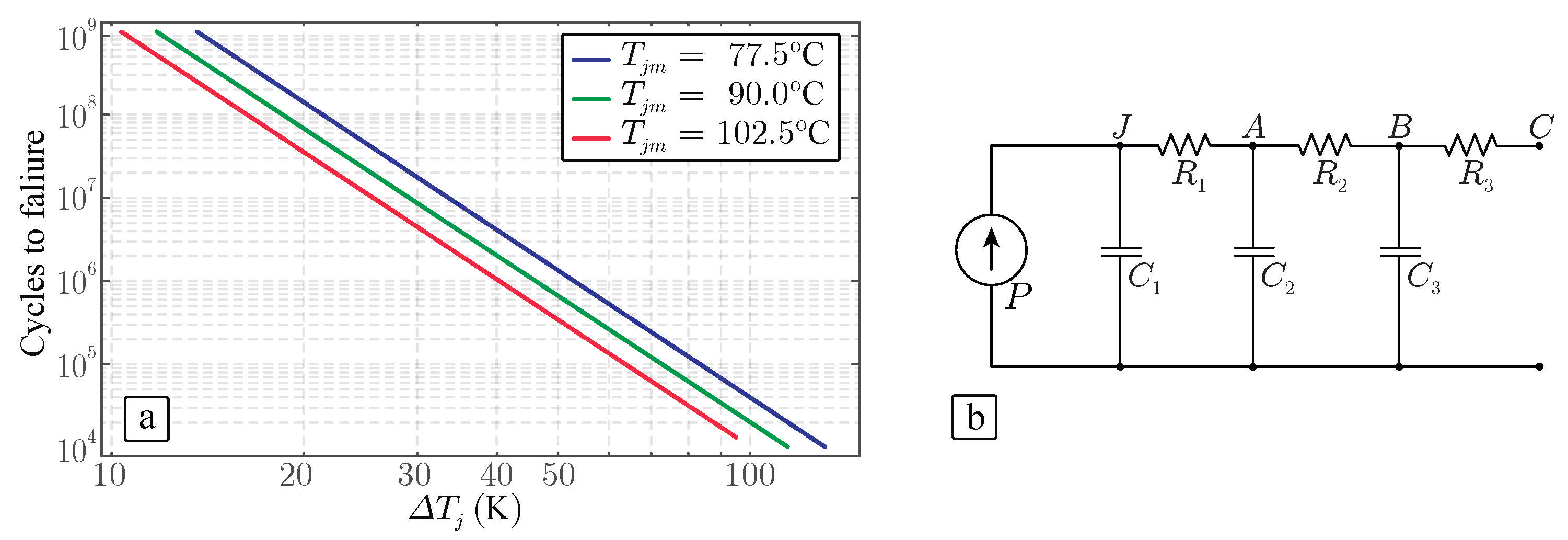
2. Power Devices Aging

Power devices are shown to be critical components in power conversion systems from a reliability point of view [18]. These components can fail for multiple reasons, with bonding wire lift-off and die-solder cracking being the most common phenomena [6,19,20,21]. In both cases, the thermal stress experienced during the operation of the power converter is the main cause of failure. Essentially, the root of the problem lies in thermal cycling, which continuously induces contraction and expansion of materials with different thermal characteristics. As a result, thermal cycling increases the thermal resistance, raising the maximum temperature reached by the materials until the end of the device’s useful life. A cross-sectional diagram of an IGBT-based power module is shown in Figure 2, where the most sensitive components, as well as derating phenomena, are highlighted.
The remaining useful lifetime (RUL) of power electronic devices has become a hot topic in recent years. Many researchers in industry and academia are focused on the development of mathematical and predictive models to describe these phenomena [20,22,23,24]. It can be stated that the number of thermal cycles a power device can undergo during its operation is a function of the operating junction temperature as well as the peak-to-peak junction temperature [25,26,27]. Among all the models available in the technical literature [3,28,29,30,31], the Coffin–Manson law is well established as a thermal derating estimator. This model is represented in (1), where the exponential relationship between the amplitude of thermal cycles, the average junction temperature, and the number of cycles to failure is modeled as follows.
As reported by several authors and summarized in [3], Coffin–Manson reliability models are dependent on the on-state duration of the devices. However, for on-states shorter than 40 ms, this effect is negligible, as it is damped by the thermal network of the devices. Since the electrical periods considered in this study imply on-states shorter than 40 ms, the unmodified Coffin–Manson law can be applied.
N f = a Δ T α e E a k B T j m
where the coefficients a, α , and E a must be obtained through experimental fitting, k B denotes Boltzmann’s constant, Δ T is the thermal cycle amplitude—defined here as the thermal ripple—and T j m is the average junction temperature. These effects are illustrated in Figure 3, using a Semikron-Danfoss (Nordborg, Denmark) power electronics module as an example [25].
The thermal network can be expanded to an arbitrary number of thermal impedance elements, but the thermal behavior of the device is generally well represented by a three-impedance model, as shown in Figure 3b. Each element of the thermal network has a physical interpretation, and each node corresponds to a real connection point within the device [32,33]. To determine the temperature variation, the power losses P in the thermal model are represented as a heat source connected to the device’s junction node J. The node C represents the case connection, where the heat sink impedance should be added. Note that since the device’s thermal capacitance is much smaller than that of the heat sink, the transient temperature response of the device can be accurately approximated by considering only the internal impedance of the device—neglecting the connection to the heat sink and the influence of nearby devices. Finally, the complete procedure to perform the RUL estimation of power devices is illustrated in the flowchart shown in Figure 4.

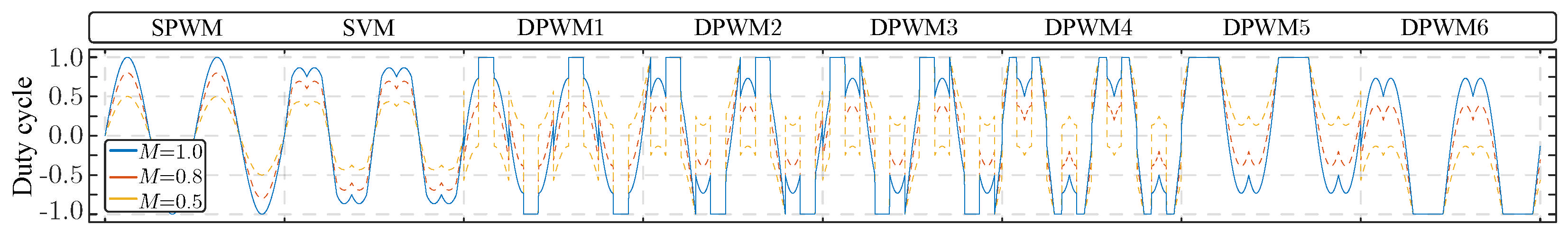
3. Carrier-Based Modulation Techniques Under Evaluation

CB-PWM methods are the mainstream solution for many industrial power applications because of their simplicity, easy implementation, and good performance. In addition, a carrier-based space vector modulation (SVM) strategy can be generated by applying a CB-PWM method with a specific common-mode injection in order to obtain different switching pulse patterns [34,35]. Therefore, the general phase voltage reference u p for the phase p to be modulated is defined as
u p = u 1 , p σ min ( u 1 ) ( 1 σ ) max ( u 1 ) ( 1 2 σ ) ,
where u 1 , p is the fundamental reference used in carrier-based sinusoidal pulse width modulation (SPWM), and the rest of the expression is the common-mode injection used to generate different switching patterns, where min ( u 1 ) and max ( u 1 ) are, respectively, the minimum and maximum values for the three-phase components (a, b, and c) of the fundamental three-phase reference vector u 1 , and σ [ 0 , 1 ] is a factor used to change the common-mode injection. Note that for σ = 0.5 , the expression in (2) is the well-known min-max injection equivalent to SVM with symmetrical minimum switching sequences, while for σ = 1 and 0, the reference u p allows a discontinuous PWM (DPWM) with positive or negative clamping. The main advantage of DPWM methods (when σ is 0 or 1) is to avoid commutations during a desired fraction of the period, as can be observed in Figure 5.
The value of σ can also be changed during a period of u 1 , as long as u c m contains only non-continuous common-mode frequency components. A way to mathematically obtain DPWM waveforms is to change σ in a periodical way as
σ ( t ) = 1 if θ c m ( t ) > π 3 , 0 if θ c m ( t ) π 3 ,
with
θ c m ( t ) = θ 1 ( t ) π 6 + ϕ M mod 2 π 3 ,
where θ 1 ( t ) is the angle of the u 1 vector in α - β coordinates, ϕ M is the DPWM phase shift, and “mod()” represents the modulo operator.
Table 1 defines the different variations of PWM methods addressed in this work, including SPWM, SVM, and different DPWM types, and Figure 5 shows the corresponding reference waveforms for these modulation methods considering different modulation indices M.

4. Impact of the Modulation Technique on the Junction Temperature of the Power Devices

The different modulation methods present in the literature were designed to enhance features such as modulation index extension and/or increased efficiency depending on the power factor, among others. However, the influence of each modulation method on the lifetime of the power devices, which is the core of this work, has not been thoroughly explored yet. The 2L-VSI topology shown in Figure 1 is the hardware test bench to check the performance of all these modulation methods.
In order to undertake this by observing the resulting average junction temperature and ripples of the power devices produced by using each modulation technique considered in Table 1, the operating conditions reported in Table 2 are used in a Matlab/Simulink (23b) using blockset PLECS 4.9 simulation environment considering a grid-connected application. The simulation analysis has been split into different scenarios, keeping the base operation conditions and sweeping the desired parameter under study. The average junction temperature and its ripple for one of the power devices of the converter is shown for all the mentioned modulation techniques.
Here are some important remarks:
  • The set of modulation techniques present symmetrical behavior with respect to upper and lower devices in each power converter’s leg. In this sense, and for better readability of the obtained results, only the upper device behavior is shown in the following subsections. The lower device presents an identical operational behavior but 180 ° shifted in each fundamental period.
  • The modulation comparison was performed under the same conventional dq-frame linear controller scheme when needed, andthe control parameters were tuned for achieve the same operational behavior in terms of bandwidth, settle time. and overshoot characteristics.
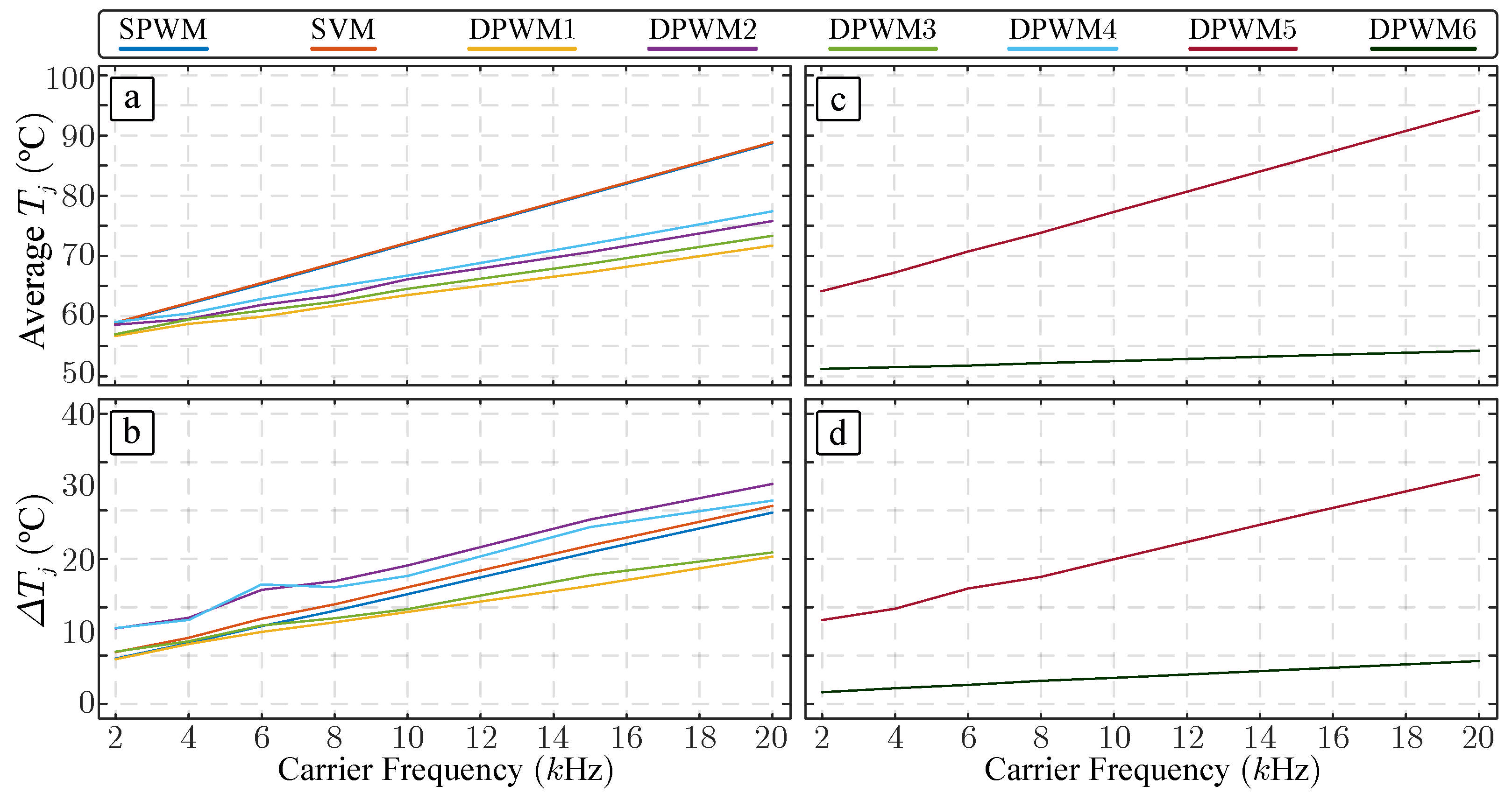
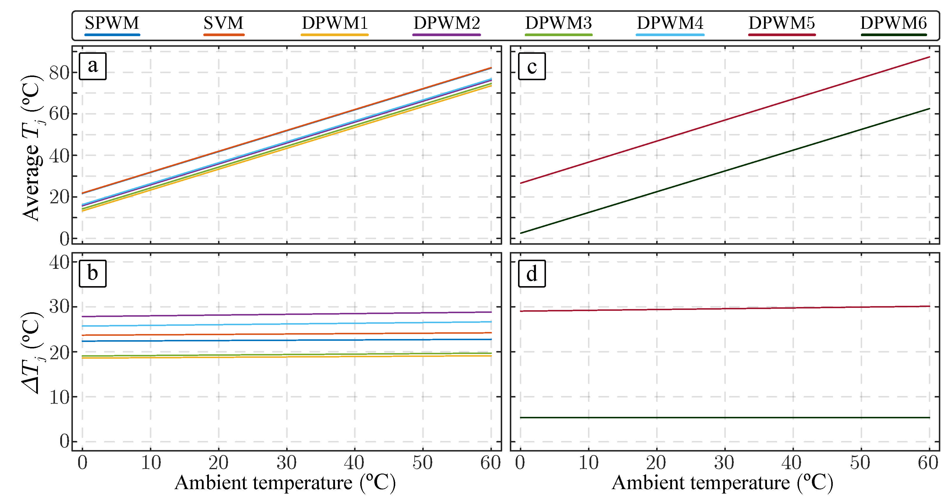
  • As shown in Figure 5, modulation techniques DPWM5 and DPWM6 clamp the output voltage to the positive (negative) bar during part of the fundamental period. This obviously creates highly unbalanced operation and thermal stress on the power devices in each phase of the power converter. Furthermore, the stress suffered by the upper device in DPWM5 is analogously reproduced in the lower device considering DPWM6 and vice versa. These techniques are only valid under fault-tolerant operations when the damage provoked in the power device is very high and, during maintenance operations, the operator continues operating the power converter. For that reason, although these techniques are shown in the obtained results, techniques DPWM5 and DPWM6 are out of analysis and therefore out the scope of this work.

4.1. Analysis Considering Different Carrier Frequencies

Taking into account the operational conditions reported in Table 2, this study first focuses on the variation in the carrier frequency.
As shown in Figure 6, the average junction temperature of a power device in each converter phase and the corresponding thermal ripple present a linear variation with increasing carrier frequency. As expected, the DPWM techniques (DPWMi, i = 1 , , 4 ) take advantage of the switching loss reduction presenting a lower average temperature than continuous PWM methods. However, from the thermal ripple point of view, DPWM2 and DPWM4 present higher values than SPWM and SVM.
Furthermore, as mentioned previously, DPWM5 and DPWM6 present an imbalance in the use of both (upper and lower) power devices. This phenomenon occurs in the average junction temperature and in their associated ripple.

4.2. Analysis Considering Different Fundamental Operation Frequencies

The system under study can be chosen for many industrial applications considering grid-connected applications and also motor drives. Therefore, the fundamental frequency may change according to the application. In this regard, considering the operational conditions reported in Table 2, several fundamental frequency cases are evaluated and the results are presented in Figure 7. As shown, the average junction temperature of the power devices remains almost constant for a wide range of fundamental frequencies. In contrast, the thermal ripple is highly dependent on the fundamental output frequency, being higher for lower fundamental frequencies. This means that motor drive applications with low fundamental frequency will present higher thermal ripples, increasing accordingly the accumulated damage of the power devices. In any case, DPWM methods obtain better performance than continuous PWM methods, presenting lower values of the average junction temperature and lower junction temperature ripples.
A great difference is shown for DPWM5 and DPWM6 regarding average T j as well as the superimposed Δ T j temperature ripple. This fact limits the applicability of these techniques to motor drive applications.

4.3. Analysis Considering Different Ambient Temperatures

The ambient temperature continuously varies during power converter operation. In this sense, considering the operational conditions reported in Table 2, the ambient temperature is modified.
As shown in Figure 8a, the average junction temperature presents a linear variation with the variation in the ambient temperature. In addition, observing Figure 8b, it is clear that the corresponding thermal ripple does not depend on the ambient temperature, including severe DPWM5 and DPWM6 techniques.

4.4. Analysis Considering Different Power Loads

The mission profile of the converter determines the power load that the converter is undergoing. The mission profile could remain constant during a portion of time or could be continuously changing depending on the application.
In any case, the impact on the average junction temperature and the thermal ripple strongly depends on the power load. In this regard, considering the other operational conditions reported in Table 2, the power load is modified. As shown in Figure 9, the average junction temperature and the corresponding thermal ripple exhibit an exponential relationship with respect to the power delivered by the converter. A distinctive operational behavior can be observed when considering the DPWM5 and DPWM6 methods, where the difference in thermal behavior is particularly pronounced.

4.5. Analysis Considering Different Power Factors

Additionally, depending on the application, it is important to consider the power factor according to the requirements of the power profile. The power factor has a significant influence on conduction and switching losses induced in the power devices and consequently on the average junction temperature and thermal ripple.
In this regard, considering the operational conditions reported in Table 2, the entire range for the power factor has been evaluated. As shown in Figure 10, the average junction temperature and the corresponding thermal ripple exhibit substantial variation depending on the power factor present in the system. An interesting result from Figure 10 is that the most suitable modulation method to be applied to reduce the average junction temperature and its ripple depends on the instantaneous value of the power factor. Notably, the DPWM6 technique (for the upper device, DPWM5 for the lower device) presents an almost flat operational behavior regarding its average temperature and ripple.

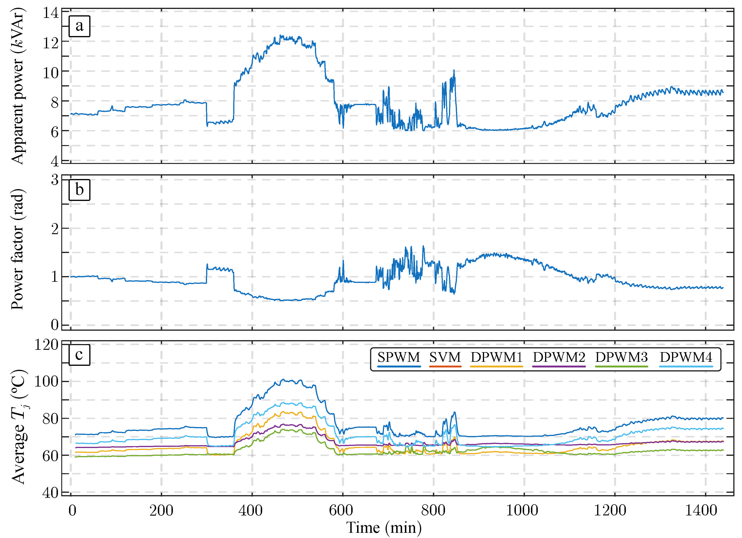
4.6. Evaluation of Case Study Example

Considering the previous discussion, a practical example is proposed in this subsection. In this regard, an auxiliary battery-tied 2L inverter connected to the grid for a solar photovoltaic application in a low-power domestic application is considered. In this case, the mission profile of the system is based on economic considerations, and some reactive power is compensated in the grid for a complete day. The mission profile is illustrated in Figure 11a,b. Figure 11c shows the obtained T j average temperature for each considered modulation excluding DPWM5 and DPWM6 for the reasons explained previously. As can be observed, DPWM3 presents superior thermal performance with lower thermal stress and flat behavior, but during a portion of time, around 900 min, DPWM1 presents better performance and lower thermal stress.
Additionally, when the whole mission profile is processed and the average T j is obtained, it is possible to apply the application procedure shown in Figure 4 to achieve an approximated value of the degradation of each power device. Table 3 reports the achieved values.
As shown, the relative damage per unit is calculated with reference to the SPWM technique since it is the modulation which presents the highest absolute damage value. In light of the results obtained in the previous subsections, it is clear that a tracking algorithm can be proposed to enforce the most appropriate modulation strategy according to the key operating parameters—namely, nominal power, power factor, and switching frequency. This technique enables real-time adaptation of the modulation technique, selecting the optimal option under varying conditions to minimize thermal stress and extend the converter’s operational lifetime. Such an approach aligns with the goal of improving overall reliability and efficiency across the entire mission profile.

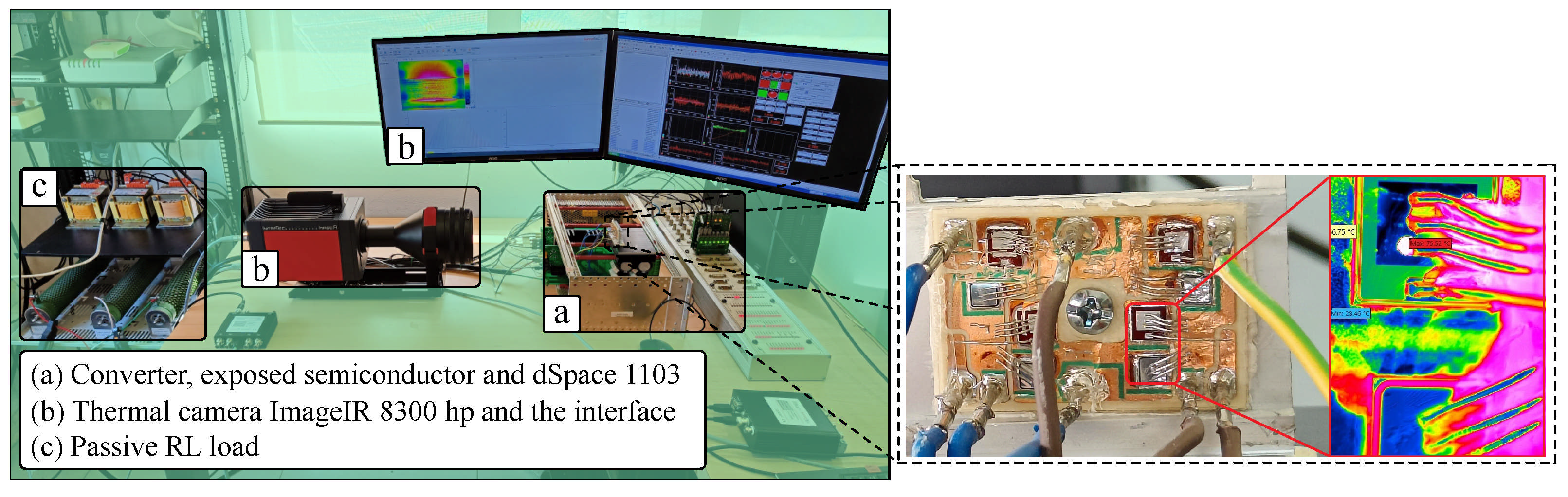
5. Experimental Results

To validate the previous results, several tests are performed on the down-scaled laboratory prototype shown in Figure 12.
To carry out the temperature analysis, a high-performance infrared ImageIR 8300 hp camera equipped with the Infratec (Dresden, Germany) WD300 microscopic lens is used. This experimental rig is composed of an IGBT-based 2L-VSI feeding a linear RL load. The IGBT devices are the SK25GH12T4 from Semikron-Danfoss, Nordborg, Denmark [36]. For measurement purposes, a power module is opened and the protective gel is carefully removed, as shown in Figure 12b. The exposed IGBT power device corresponds to the lower device of phase c in the 2L-VSI converter. The remaining passive elements, as well as operating parameters, are reported in Table 4. The lower rating of the experimental results compared to the simulation conditions is due to the absence of the filling gel, which limits the voltage and loss dissipation capabilities of the power module. The comparison with the simulation is for trend validation rather than absolute values. For the operation of the converter, the conventional closed-loop voltage-oriented control method is implemented using the conventional synchronous d q frame control strategy. All the modulation techniques shown in Table 1 are evaluated. The power converter is powered using a programmable DC source, and the implementation of the linear control scheme with the corresponding modulation technique is implemented on the dSPACE DS1103 control platform. It should be noted that the effect of the controls is outside the scope of this study and the performance is compared at the same output voltage and current conditions for all modulations. To evaluate the junction temperature T j , an operating point given by the references i d = 4 AA and i q = 0 AAr is evaluated (for safety and practical reasons in the laboratory), which represents an active power delivered of 240 W with a unity power factor. After the required time to achieve steady state in temperature terms (approximately 30 min), all experiments are evaluated considering the average measured junction temperature T j and the peak-to-peak T j evolution (thermal ripple Δ T j ).
Figure 13 and Figure 14 show the instantaneous junction temperature T j ( t ) and the phase current in the RL load applying each modulation technique. In order to highlight the junction temperature T j signal acquisition, the heat sink in the power module is reduced. In the figures, the resulting duty cycle signal for each evaluated modulation technique is also represented. As clearly observed in Figure 13 and Figure 14, the achieved time-varying T j varies in mean value and ripple according to the applied modulation technique, as expected. In all cases, continuous modulation techniques (SPWM and SVM) exhibit both higher average junction temperature and a junction temperature ripple around 4 degrees. On the other hand, all DPWM methods present similar average temperature but much lower than the value obtained by applying the SPWM or SVM methods. Also, the ripple junction temperature is maintained around 5 degrees, although DPWM3 presents slightly lower Δ T j .

6. Conclusions

The evaluation of thermal behavior in power electronics converters is essential to ensure operational safety and assess reliability. This thermal condition is influenced by several factors, including ambient temperature, mission profile, and the operating principle adopted by the power converter. This paper evaluates the impact of the selected modulation technique on the resulting average junction temperature and ripple to select the most appropriate technique according to various criteria. This study concludes that power load and power factor are the most critical parameters, while ambient temperature and switching frequency exhibit linear behavior. The results clearly demonstrate that the use of DPWM methods reduces switching losses, with a corresponding decrease in average junction temperature, while maintaining junction temperature ripple within acceptable values. Finally, it should be highlighted that the different variations in DPWM with symmetrical discontinuities (DPWM [1–4]) play an important role in junction temperature variation in terms of phase shift between voltage and current, albeit with minor changes. Finally, there is an opportunity to develop a modulation-based tracking method for implementing an appropriate modulation technique based on the operational point of the power converter.

Author Contributions

Conceptualization, A.M.A., J.I.L. and C.A.R.; software, C.A.R., J.G.B. and A.S.-V.; formal analysis, A.M.A. and J.I.L.; research, A.M.A., J.I.L., C.A.R., J.G.B., A.S.-V., S.K., A.H.W.-V. and G.B.; resources, C.A.R. and S.K.; writing—original draft preparation, A.M.A., J.I.L. and C.A.R.; writing—review and editing, A.M.A., J.I.L., C.A.R., J.G.B., A.S.-V., S.K., A.H.W.-V. and G.B.; visualization, A.M.A. and A.S.-V.; supervision, A.M.A., J.I.L. and C.A.R.; project administration, C.A.R.; funding acquisition, C.A.R. All authors have read and agreed to the published version of the manuscript.

Funding

The authors appreciate financial support provided by Ministerio de Ciencia e Innovación under the project TED2021-130613B-I00 and PID2023-152292OB-I00 as well as “UE-Ministerio de Hacienda y Función Publica-Fondos Europeos-Junta de Andalucía–Consejería de Universidad, Investigación e Innovación project 2024-31824-1828102303”, SERC Chile (ANID/FONDAP/1523A0006), AC3E (ANID/BASAL/AFB240002), ANID/Fondecyt Regular/1240537, and the Ningbo Science Foundation Project 2023J025.

Data Availability Statement

The original contributions presented in this study are included in the article. Further inquiries can be directed to the corresponding author.

Conflicts of Interest

The authors declare that the research was conducted in the absence of any commercial or financial relationships that could be construed as a potential conflict of interest.

References

  1. Chung, H.; Wang, H.; Blaabjerg, F.; Pecht, M. Reliability of Power Electronic Converter Systems; Energy Engineering, Institution of Engineering and Technology: London, UK, 2015. [Google Scholar]
  2. Peyghami, S.; Wang, Z.; Blaabjerg, F. A Guideline for Reliability Prediction in Power Electronic Converters. IEEE Trans. Power Electron. 2020, 35, 10958–10968. [Google Scholar] [CrossRef]
  3. Wang, H.; Blaabjerg, F. Power Electronics Reliability: State of the Art and Outlook. IEEE J. Emerg. Sel. Top. Power Electron. 2021, 9, 6476–6493. [Google Scholar] [CrossRef]
  4. Peyghami, S.; Blaabjerg, F.; Palensky, P. Incorporating Power Electronic Converters Reliability Into Modern Power System Reliability Analysis. IEEE J. Emerg. Sel. Top. Power Electron. 2021, 9, 1668–1681. [Google Scholar] [CrossRef]
  5. Wang, H.; Liserre, M.; Blaabjerg, F. Toward Reliable Power Electronics: Challenges, Design Tools, and Opportunities. IEEE Ind. Electron. Mag. 2013, 7, 17–26. [Google Scholar] [CrossRef]
  6. Wang, B.; Cai, J.; Du, X.; Zhou, L. Review of power semiconductor device reliability for power converters. CPSS Trans. Power Electron. Appl. 2017, 2, 101–117. [Google Scholar] [CrossRef]
  7. Liserre, M.; Buticchi, G.; Leon, J.I.; Marquez Alcaide, A.; Raveendran, V.; Ko, Y.; Andresen, M.; Monopoli, V.G.; Franquelo, L. Power Routing: A New Paradigm for Maintenance Scheduling. IEEE Ind. Electron. Mag. 2020, 14, 33–45. [Google Scholar] [CrossRef]
  8. Monopoli, V.G.; Marquez, A.; Leon, J.I.; Liserre, M.; Buticchi, G.; Franquelo, L.G.; Vazquez, S. Applications and Modulation Methods for Modular Converters Enabling Unequal Cell Power Sharing: Carrier Variable-Angle Phase-Displacement Modulation Methods. IEEE Ind. Electron. Mag. 2022, 16, 19–30. [Google Scholar] [CrossRef]
  9. Li, Y.; Li, Y.W. The Evolutions of Multilevel Converter Topology: A Roadmap of Topological Invention. IEEE Ind. Electron. Mag. 2022, 16, 11–18. [Google Scholar] [CrossRef]
  10. Leon, J.I.; Kouro, S.; Franquelo, L.G.; Rodriguez, J.; Wu, B. The Essential Role and the Continuous Evolution of Modulation Techniques for Voltage-Source Inverters in the Past, Present, and Future Power Electronics. IEEE Trans. Ind. Electron. 2016, 63, 2688–2701. [Google Scholar] [CrossRef]
  11. Alcaide, A.M.; Buticchi, G.; Chub, A.; Dalessandro, L. Design and Control for High-Reliability Power Electronics: State-of-the-Art and Future Trends. IEEE J. Emerg. Sel. Top. Ind. Electron. 2024, 5, 50–61. [Google Scholar] [CrossRef]
  12. Ibrahim, A.; Salem, M.; Kamarol, M.; Delgado, M.T.; Desa, M.K.M. Review of Active Thermal Control for Power Electronics: Potentials, Limitations, and Future Trends. IEEE Open J. Power Electron. 2024, 5, 414–435. [Google Scholar] [CrossRef]
  13. Ni, Z.; Lyu, X.; Yadav, O.P.; Singh, B.N.; Zheng, S.; Cao, D. Overview of Real-Time Lifetime Prediction and Extension for SiC Power Converters. IEEE Trans. Power Electron. 2020, 35, 7765–7794. [Google Scholar] [CrossRef]
  14. Dusmez, S.; Ali, S.H.; Heydarzadeh, M.; Kamath, A.S.; Duran, H.; Akin, B. Aging Precursor Identification and Lifetime Estimation for Thermally Aged Discrete Package Silicon Power Switches. IEEE Trans. Ind. Appl. 2017, 53, 251–260. [Google Scholar] [CrossRef]
  15. Jang, Y.C.; Kim, S.S.; Ha, M.W.; Kim, Y.S. Accelerated Degradation of IGBTs Due to High Gate Voltage at Various Temperature Environments. IEEE Trans. Device Mater. Reliab. 2020, 20, 731–736. [Google Scholar] [CrossRef]
  16. Ugur, E.; Dusmez, S.; Akin, B. An Investigation on Diagnosis-Based Power Switch Lifetime Extension Strategies for Three-Phase Inverters. IEEE Trans. Ind. Appl. 2019, 55, 2064–2075. [Google Scholar] [CrossRef]
  17. Sun, P.; Luo, H.; Dong, Y.; Li, W.; He, X.; Chen, G.; Yang, E.; Dong, Z. Online junction temperature extraction with turn-off delay time for high power IGBTs. In Proceedings of the 2014 IEEE Energy Conversion Congress and Exposition (ECCE), Pittsburgh, PA, USA, 14–18 September 2014; pp. 4016–4021. [Google Scholar] [CrossRef]
  18. Falck, J.; Felgemacher, C.; Rojko, A.; Liserre, M.; Zacharias, P. Reliability of Power Electronic Systems: An Industry Perspective. IEEE Ind. Electron. Mag. 2018, 12, 24–35. [Google Scholar] [CrossRef]
  19. Ciappa, M. Selected failure mechanisms of modern power modules. Microelectron. Reliab. 2002, 42, 653–667. [Google Scholar] [CrossRef]
  20. Dornic, N.; Ibrahim, A.; Khatir, Z.; Degrenne, N.; Mollov, S.; Ingrosso, D. Analysis of the aging mechanism occurring at the bond-wire contact of IGBT power devices during power cycling. Microelectron. Reliab. 2020, 114, 113873. [Google Scholar] [CrossRef]
  21. Yu, X.; Kong, J.; Wang, N.; Zhang, K.; Blaabjerg, F.; Zhou, D. A Review on Junction Temperature and ON-state Voltage Condition Monitoring of Power Semiconductor Devices. Chin. J. Electr. Eng. 2025, 11, 17–37. [Google Scholar] [CrossRef]
  22. Kovačević, I.F.; Drofenik, U.; Kolar, J.W. New physical model for lifetime estimation of power modules. In Proceedings of the 2010 International Power Electronics Conference-ECCE ASIA-, Sapporo, Japan, 21–24 June 2010; pp. 2106–2114. [Google Scholar] [CrossRef]
  23. Lutz, J.; Schlangenotto, H.; Scheuermann, U.; De Doncker, R. Semiconductor Power Devices: Physics, Characteristics, Reliability; Springer Science & Business Media: Berlin/Heidelberg, Germany, 2011. [Google Scholar]
  24. Yang, K.; Liu, B.; Tan, H.; Xu, P.; Chen, J.; Tang, T.; Song, W. A Converter-Level Junction Temperature Monitoring Method for IGBT Based on the Turn-off Gate Electric Quantities. IEEE Trans. Power Electron. 2025, 1–11. [Google Scholar] [CrossRef]
  25. Wintrich, A.; Nicolai, U.; Tursky, W.; Reimann, T. Semikron Application Manual Power Semiconductors; ISLE: Ilmenau, Germany, 2011. [Google Scholar]
  26. Huang, H.; Mawby, P.A. A Lifetime Estimation Technique for Voltage Source Inverters. IEEE Trans. Power Electron. 2013, 28, 4113–4119. [Google Scholar] [CrossRef]
  27. Zhou, D.; Wang, H.; Blaabjerg, F. Mission Profile Based System-Level Reliability Analysis of DC/DC Converters for a Backup Power Application. IEEE Trans. Power Electron. 2018, 33, 8030–8039. [Google Scholar] [CrossRef]
  28. Norris, K.C.; Landzberg, A.H. Reliability of Controlled Collapse Interconnections. IBM J. Res. Dev. 1969, 13, 266–271. [Google Scholar] [CrossRef]
  29. Bayerer, R.; Herrmann, T.; Licht, T.; Lutz, J.; Feller, M. Model for Power Cycling lifetime of IGBT Modules-various factors influencing lifetime. In Proceedings of the 5th International Conference on Integrated Power Electronics Systems, Nuremberg, Germany, 11–13 March 2008; pp. 1–6. [Google Scholar]
  30. Yang, S.; Xiang, D.; Bryant, A.; Mawby, P.; Ran, L.; Tavner, P. Condition Monitoring for Device Reliability in Power Electronic Converters: A Review. IEEE Trans. Power Electron. 2010, 25, 2734–2752. [Google Scholar] [CrossRef]
  31. Busca, C.; Teodorescu, R.; Blaabjerg, F.; Munk-Nielsen, S.; Helle, L.; Abeyasekera, T.; Rodriguez, P. An overview of the reliability prediction related aspects of high power IGBTs in wind power applications. Microelectron. Reliab. 2011, 51, 1903–1907. [Google Scholar] [CrossRef]
  32. Gerstenmaier, Y.C.; Wachutka, G. The minimal set of parameters for exact dynamic thermal models. In Proceedings of the 2008 14th International Workshop on Thermal Inveatigation of ICs and Systems, Rome, Italy, 24–26 September 2008; pp. 70–75. [Google Scholar] [CrossRef]
  33. Berger, J.G.; Rojas, C.A.; Wilson-Veas, A.H.; Bugueño, R.A.; Peralta, A.; Salinas, S.; Marín, J.; Young, H.; Callegaro, L. On the Experimental Verification of Electrothermal Modeling of GaN-HEMT-Based DC–DC Converters. IEEE Trans. Power Electron. 2025, 40, 5518–5530. [Google Scholar] [CrossRef]
  34. Hava, A.; Kerkman, R.; Lipo, T. A high-performance generalized discontinuous PWM algorithm. IEEE Trans. Ind. Appl. 1998, 34, 1059–1071. [Google Scholar] [CrossRef]
  35. Holmes, D.; Lipo, T. Pulse Width Modulation for Power Converters: Principles and Practice; IEEE Press Series on Power Engineering; Wiley: Hoboken, NJ, USA, 2003. [Google Scholar]
  36. Wintrich, A.; Nicolai, U.; Tursky, W.; Tobias, R. Application Manual Power Semiconductors; SEMIKRON International GmbH: Nurnberg, Germany, 2015. [Google Scholar]
Figure 1. Grid connected two-level three-phase voltage source inverter (2L-VSI) diagram.
Electronics 14 02934 g001
Figure 2. Cross section of a conventional power module, and typical faults and their location.
Electronics 14 02934 g002
Figure 3. (a) Temperature cycle capability characteristic N f for a standard Semikron IGBT module. (b) Generic Cauer thermal network of a single power electronics device, without heat sink [25].
Electronics 14 02934 g003
Figure 4. Complete application procedure for power devices’ lifetime expectancy calculation.
Electronics 14 02934 g004
Figure 5. Time waveform of the normalized reference voltages generated by the different modulations under study.
Electronics 14 02934 g005
Figure 6. Simulation results using base parameters (Table 2) for upper device in the power converter’s leg and considering a sweep in the carrier frequency: (a,c) Average junction temperature T j , (b,d) maximum junction temperature ripple in a fundamental cycle Δ T j .
Electronics 14 02934 g006
Figure 7. Simulation results using base parameters (Table 2) for upper device in the power converter’s leg and considering a sweep in the fundamental frequency: (a,c) Average junction temperature T j , (b,d) maximum junction temperature ripple in a fundamental cycle Δ T j .
Electronics 14 02934 g007
Figure 8. Simulation results using base parameters (Table 2) for upper device in the power converter’s leg and considering a sweep in the ambient temperature: (a,c) Average junction temperature T j , (b,d) maximum junction temperature ripple in a fundamental cycle Δ T j .
Electronics 14 02934 g008
Figure 9. Simulation results using base parameters (Table 2) for upper device in the power converter’s leg and considering a sweep in the power load: (a,c) Average junction temperature T j , (b,d) maximum junction temperature ripple in a fundamental cycle Δ T j .
Electronics 14 02934 g009
Figure 10. Simulation results using base parameters (Table 2) for upper device in the power converter’s leg and considering a sweep in the power factor: (a,c) Average junction temperature T j , (b,d) maximum junction temperature ripple in a fundamental cycle Δ T j .
Electronics 14 02934 g010
Figure 11. Estimation of the average T j temperature of the upper semiconductor of the phase-a of the inverter for the mission profile shown in (a) Apparent power (KVar). (b) Power factor (rad). (c) Average T j (°C).
Electronics 14 02934 g011
Figure 12. Experimental setup used in this work including the exposed semiconductor for measuring purposes.
Electronics 14 02934 g012
Figure 13. Experimental results applying continuous PWM methods where i d = 4 AA and i q = 0 AAr. (a,b), Obtained T j in the experimental rig. (c,d), Applied duty cycle in the power converter. (e,f), Output current of the converter.
Electronics 14 02934 g013
Figure 14. Experimental results applying DPWM methods where i d = 4 AA and i q = 0 AAr. From (ad), Obtained T j in the experimental rig. From (eh), Applied duty cycle in the power converter. From (il), Output current of the converter.
Electronics 14 02934 g014
Table 1. Different modulations used in this work.
Cases of StudyModulation TypeAcronym
Continuous
modulation methods
Sinusoidal PWMSPWM
Space vector modulationSVM
Discontinuous
modulation
methods
30 ° DPWMDPWM1
60 ° DPWMDPWM2
60 ° + 30 ° phase-shift DPWMDPWM3
60 ° 30 ° phase-shift DPWMDPWM4
120 ° DPWM with positive clampingDPWM5
120 ° DPWM with negative clampingDPWM6
Table 2. Base parameters for simulation analysis.
ParameterSymbolValueParameterSymbolValue
DC voltage V d c 800 V Nominal powerS10 kVA
Load inductanceL5 m H Line frequency f o 50 Hz
Carrier frequency f s 10 k Hz Ambient temperature T a 50 °C
Power factor φ 0 rad
Table 3. Estimated RUL degradation for studied mission profile case.
AcronymAbsolute DamageRelative Damage (%)
SPWM 2.49 × 10 5 100
DPWM1 2.59 × 10 6 10.40
DPWM2 9.04 × 10 7 3.63
DPWM3 5.21 × 10 7 2.09
DPWM4 5.09 × 10 6 20.45
Table 4. Parameters for experiments.
ParameterValueParameterValue
DC voltage [ V d c ] 250 V Load inductance [ L ] 15 m H
Load resistor [ R ] 10 Ω Output frequency [ f o ] 1 Hz
Ambient temperature [ T a ] 25 °CSwitching frequency [ f s w ] 10 k Hz
IR camera frequency [ f s t ] 200 Hz dSPACE frequency [ f s ] 10 k Hz
Disclaimer/Publisher’s Note: The statements, opinions and data contained in all publications are solely those of the individual author(s) and contributor(s) and not of MDPI and/or the editor(s). MDPI and/or the editor(s) disclaim responsibility for any injury to people or property resulting from any ideas, methods, instructions or products referred to in the content.

