Abstract
Dynamic on-resistance (RON) of commercial GaN on Si normally off high-electron-mobility transistor (HEMT) devices is a very important parameter because it is responsible for conduction losses that limit the power conversion efficiency of high-power switching converters. Due to charge trapping effects, dynamic RON is always higher than in DC, a behavior known as current collapse. To study how short-time dynamics of charge trapping and release affects RON we use rectangular 0–5 V gate voltage pulses with durations in the 1 μs to 100 μs range. Measurements are first carried out for single pulses of increasing duration, and it is found that RON depends on both pulse duration and drain current ID, being higher at shorter pulse durations and lower ID. For a train of five pulses, RON decreases with pulse number, reaching a steady state after a time interval of 100 μs. The response to a five pulses train is compared to that of a square-wave signal to study the time evolution of RON toward a dynamic steady state. The DC RON is also measured, and it is a factor of ten smaller than dynamic RON at the same ID. This confirms that a reduction in trapped charges takes place in DC as compared to the square-wave switching operation. Additional off-state stress tests at VDS = 55 V reveal the presence of residual surface traps in the drain access region, leading to four times increase in RON in comparison to pristine devices. Finally, the dynamic RON is also measured by the double-pulse test (DPT) technique with inductive load, giving a good agreement with results from single-pulse measurements.
1. Introduction
Gallium nitride (GaN) high-electron-mobility transistors (HEMTs) are a hot topic for scientific research and industrial applications due to their capability to drive high current with low dynamic on-resistance (RON) and to withstand high voltages [1,2]. They are used for high power switching circuits in the electric vehicles automotive industry or for RF applications [3]. However, to cut production cost and to exploit the advantages of integration these GaN HEMTs are grown on Si wafers. As Si and GaN have a 17% lattice mismatch, this leads to a significant concentration of crystal defects in the heterostructure, acting as trap centers for charge carriers [4]. These trapping centers and their relevant effects play an important role in the degradation of dynamic performance and limit long-term reliability of these HEMTs through peculiar failure modes. Updated and comprehensive reviews on charge carrier trapping and release mechanisms in GaN on Si heterostructure can be found in [5,6].
Figure 1 illustrates the simplified cross-section of a typical normally off p-GaN gate [7] HEMT device with traps distribution and their effects on dynamic electrical parameters. For simplicity, the details of the necessary buffer layer to aid Si to GaN transition and reduce crystal defects concentration during the epitaxial growth are not indicated.
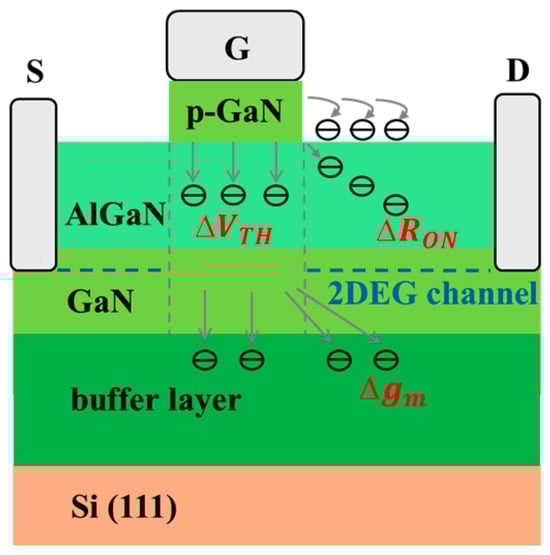
Figure 1.
Schematic representation of surface and bulk traps in a normally off p-GaN HEMT affecting threshold voltage VTH, dynamic RON, and transconductance gm.
In a hard switching operation at relatively low drain to source blocking voltages VDS (less than 100 V) and drain currents ID (less than 1 A), as is the case of our study, the horizontal electric field during the off-time and the off-time itself are not sufficient to induce barrier surface/interface trapping in the drain access region [8]. For the same reason, during the off-to-on transition and the on-time, accelerated electrons in the two-dimensional electron gas (2DEG) channel cannot acquire sufficient kinetic energy to overcome the potential barrier and become trapped in the AlGaN barrier of the drain access region, i.e., the generation of hot electrons [9,10] can be ruled out. Hence the main contributions to the observed changes in RON must be attributed to electrons of the 2DEG channel that become trapped within the channel itself during the on-time together with electrons trapped in the buffer layer during the off-time, both under the gate and in the drain access region [11]. In fact, trapped electrons in the channel are responsible for scattering, decreasing free electrons mobility and leading to an increase in RON. Trapped electrons in the buffer layer under the channel during off-time can be considered as being located uniformly in the whole device’s active area. They also affect the RON, as well as the threshold voltage VTH and the transconductance gm, because they act as a back gate that negatively biases the device giving an increased RON [11].
Of course, during the switching operation, the reverse process also takes place, i.e., the electric field-assisted trapped charge release mostly during the off-time and a dynamic steady state must be established in the device through a dynamic balance between charge trapping and release. Understanding charge trapping and release dynamic mechanisms and their influence on RON is critical for ensuring long-term reliability and performance stability of these devices.
Datasheets of commercial GaN HEMT devices usually report the DC or static RON only, but in a switching operation, the dynamic on-resistance RON is more relevant because it determines conduction losses that limit the power conversion efficiency of high-power switching converters. Dynamic RON is invariably higher than the static one, leading to an increase in switching and conduction losses and longer switching times. This behavior is also known as a current collapse [12].
In this paper we address the time evolution of RON of commercial normally off GaN HEMT devices operated in hard switching mode with resistive load using rectangular gate voltage pulses. Measurements are first conducted for single pulses of increasing duration from 1 μs to 100 μs and then for a train of five pulses to analyze short-time transient switching behavior and to check if and how dynamic RON evolves with pulse number trough trapped charge accumulation. These results are compared to those of steady-state switching with a square-wave gate voltage at much longer times, and to the DC RON measured over a time interval of 30 min. To check the possible influence on dynamic RON of trapped electrons at surface/interface traps in the drain-side access region DC, off-state stress tests are conducted, resulting in an appreciable increase in RON in comparison to the one of pristine device. Finally, we use the double-pulse test (DPT) method with inductive load to measure RON and compare results to those for single-pulse measurements. The presented results give useful insights into the short timescale dynamic and steady-state behavior of RON.
The main advantage of our method, compared to more complex circuits as half and full bridge topologies used in switching converters, is simplicity. However, the latters give more accurate results because the HEMT devices are operated under real load conditions, like those found in electric vehicles with batteries or electric motors.
2. Materials and Methods
The circuit used for the measurements is shown in Figure 2. The drain load can be a simple resistor RD, or an air core inductor shunted by a fast power Schottky diode (MBRS1100) for the measurements conducted by the DPT method. The transistor is a commercial normally off GaN HEMT device produced by ST (SGT120R65AL, 650 V, RON = 75 mΩ typ., 15 A). The typical threshold voltage is 1.8 V and the absolute maximum rating for the positive VGS is 7 V. Hence, to drive it deeply into the ohmic region without risk of gate junction breakdown, we use rectangular gate voltage pulses having amplitude 0–5 V.
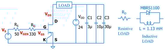
Figure 2.
Circuit schematic used for measurements. The drain load can be resistive or inductive for the DPT method.
The rectangular voltage pulses for driving the gate are provided by an arbitrary signal generator (Digilent Analog Discovery 2 multi functions programmable board, recommended output current of 10 mA at ±5 V and maximum absolute rating of 50 mA at ±5.8 V of analog output voltage). The free software WaveForms, which can be downloaded from the Digilent website at https://digilent.com/reference/software/waveforms/waveforms-3/start (accessed on 8 June 2025), is used to generate the rectangular voltage pulses. The gate series resistor is added to comply with the current limit of the arbitrary signal generator. The chosen 330 Ω value ensures a good trade-off between the gate charge/discharge peak current required to the driver and the fast switching time of the GaN HEMT in response to a rectangular gate voltage. We check in advance that even for the minimum rectangular pulse duration of 1 μs, the VGS reaches 5 V, and the drain current reaches its steady-state value, as shown in Figure 3a.
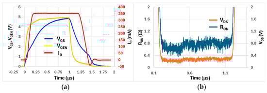
Figure 3.
Response to a single rectangular pulse of 1 μs duration for a drain current of 350 mA. (a) gate-source voltage VGS, generator voltage VGEN, and drain current ID. (b) dynamic RON and drain-source voltage VDS.
For the case of resistive drain load, the voltages across the gate and drain resistors, whose value is accurately measured in advance, are acquired by a four channels oscilloscope (Tektronix MSO54) through 1X accurately compensated probes. The drain current is calculated as ID(t) = [VDD(t) – VDS(t)]/RD. The dynamic on-resistance RON is calculated as VDS(t)/ID(t), giving the time evolution during the on-time. Where single values of RON are quoted, these are the nominal resistance values taken, for convenience, in correspondence to 90% of the on-time pulse duration. The switched drain current can be set by changing VDD (6 V or 24 V) and RD to obtain ID ranging from 100 mA to 750 mA.
For the case of the DPT method with inductive load, the drain current ID(t) and the inductor current IL(t) are measured by means of two current probes, Teledyne LeCroy T3CP100-2, whose output is connected to the Tektronix MSO54 oscilloscope. The dynamic on-resistance RON is again calculated as VDS(t)/ID(t).
As during the on-state of the device VDS can be in the hundreds of mV range, the oscilloscope is set to high-resolution mode, exploiting the maximum available bit depth (16 bits). Furthermore, to reduce noise, the bandwidth is limited for all four channels of the oscilloscope. For practical convenience, the measurement circuit is implemented on a breadboard, ensuring the wire connections are as short as possible to minimize parasitic effects. Before each measurement, the gate and drain terminals of the device are shorted to the ground for two minutes to release any trapped charge leftover from the previous measurement and re-establish pristine condition avoiding the presence of any form of ‘memory effect.’ Measurements are conducted on several SGT120R65AL devices but for consistency the reported results are for the same single device. The voltage measurement errors can be assumed to be 5%, but for better clarity, error bars are not indicated in the graphs, displaying single numerical values. A picture of the measurement setup and further practical details are given in [8].
3. Results and Discussion
The response to a single rectangular voltage pulse of 1 μs duration, that is, the minimum duration used for the measurements, for resistive load and ID = 350 mA is shown in Figure 3a.
The Vs (see Figure 2) rise/fall times under no load can be assumed to be 100 ns and its RS = 50 Ω internal output series resistance, set by an external jumper on the Analog Discovery 2 board, adds to the 330 Ω gate resistor. Hence the total resistance seen by the gate capacitance is 380 Ω. The 50 Ω internal output resistance gives VGEN smoothed out rise and falling edges. It can be noticed that VGS still reaches 5 V at the end of the pulse and that the ID trace switches very abruptly and has a flat top meaning that ID can reach its steady-state value. The ringing on the falling edge of ID is due to unavoidable parasitic inductive effects, but its maximum amplitude of about 50 mA is small in comparison to the switched ID = 350 mA. This demonstrates that by keeping wire connections on the breadboard as short as possible, parasitic effects are kept to a minimum. Figure 3b shows that VDS also switches quite abruptly and has an almost flat bottom. The ratio VDS(t)/ID(t) gives the dynamic RON(t) trace that has a slightly increasing trend and exhibits some noise. The quoted value for RON is the average value taken at 90% of RON(t) duration, that in this case, is 0.8 Ω.
Figure 4 shows the time evolution of RON together with ID and VDS for a longer 5 μs pulse duration and again ID = 350 mA. An initial increasing trend with time for RON is evident and then it reaches a steady state. This behavior can be explained with the fact that a 5 μs pulse duration is comparable to the short timescale for trapping effects of electrons in the 2DEG channel to take place and be effective.
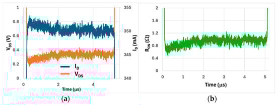
Figure 4.
Response to a single rectangular pulse of 5 μs duration for a drain current of 350 mA. (a) drain-source voltage VDS and drain current ID and (b) dynamic RON.
In fact, trapping of electrons in trap centers located in the 2DEG channel are responsible for scattering, decreasing free electrons mobility and channel conductivity and resulting in current collapse with an associated increase in RON. On the other hand, the release of electric field-assisted electrons from these centers must be associated with a current collapse reduction and a decrease in RON. When an equilibrium between trapping and release is established, then RON should remain constant with time. In addition, the ratio of empty to filled traps must be higher at low ID current, because electron trapping is proportional to the free charge carrier concentration while electron release is not dependent on it [13].
The values of RON as a function of pulse duration and for different drain currents are reported in Figure 5. It can be noticed that at low currents of 100 mA and 350 mA, trapping effects with increasing RON prevail for short pulse durations (1 μs and 5 μs) and then for longer pulse durations, RON decreases steadily. However, for a high current of 750 mA, RON decreases steadily with pulse duration. This behavior can be explained by the fact that with a finite concentration of traps in the 2DEG channel, the capture probability increases with increasing free carrier concentration [13], i.e., drain current, and hence the average trapping time, becomes shorter than 1 μs. RON at 750 mA reaches a constant value at 10 μs pulse duration, while for lower currents it takes 50 μs, which is five times longer. This means that the average release time is longer for a lower ID. RON at 100 mA has the lowest constant value, because the ratio of empty to filled traps is higher at low current. When the device is operated at much higher switching currents, these effects are less evident because the drain current plays an important role in the trapping process, leading to higher RON values.
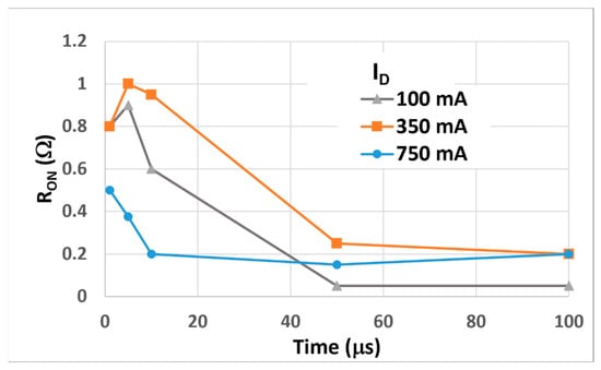
Figure 5.
Dynamic RON as a function of pulse duration for ID = 100 mA, 350 mA, and 750 mA.
To study the cumulative effect of the traps on drain current conduction and RON, we use a train of five gate voltage pulses with 50% duty cycle. An important difference with the single-pulse case is that during each on-to-off transition, electrons in the channel are pushed towards the buffer layer where they become trapped by bulk traps. When the device is driven back to the on-state by the next pulse of the train, these trapped electrons act as a “back gate” with negative bias, affecting threshold gate voltage VTH. Bulk traps in the buffer layer can be assumed to be distributed in the whole device active area; hence, the “back gate” is extended in the gate-to-drain region as well, and this affects also dynamic RON [11].
The time evolution of ID and VDS during a train of five pulses of 10 μs duration each, corresponding to a 50 kHz square wave, is shown in Figure 6 for a nominal drain current of 100 mA. The expanded vertical scale reveals that the drain current increases and the drain voltage decreases with pulse number, both reaching a sort of steady-state regime starting from the third pulse. Similar behavior is observed at ID = 350 mA but not at ID = 750 mA. The dynamic RON vs. pulse number reported in Figure 7 for comparison at ID = 100 mA, 350 mA, and 750 mA is almost constant with the pulse number for ID = 750 mA. At lower currents, RON is decreasing with pulse number, a behavior like the case of single voltage pulses reported previously in Figure 5.
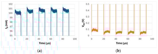
Figure 6.
Response to a train of five pulses of 10 μs duration each for nominal ID = 100 mA. (a) Drain current ID, (b) drain-source voltage VDS.
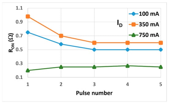
Figure 7.
Dynamic RON vs. gate voltage pulse number for ID = 100 mA, 350 mA, and 750 mA. The pulse duration is 10 μs.
It is worth noticing from comparing Figure 5 and Figure 7 that RON for the fifth pulse of the train is always higher than the one for an equivalent single pulse with 100 μs duration. This means that the release of electrons is less effective during a switching operation at higher repetition frequency.
The effect of the traps on the threshold gate voltage VTH vs. the pulse number is also investigated. By plotting the drain current as a function of the gate voltage for the same pulse, the corresponding graph shows a sort of hysteresis between the rising and falling edges of the drain current, as shown in Figure 8a for ID = 100 mA, where the negative values of ID during the falling edge are due to parasitic inductive effects.
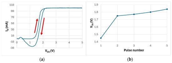
Figure 8.
(a) Current hysteresis ID vs. VGS between rising (up arrow) and falling (down arrow) edges at 100 mA, (b) threshold voltage VTH for the rising edge at 10 mA vs. pulse number.
The threshold gate voltage VTH taken at ID = 10 mA during a rising edge vs. the pulse number is reported in Figure 8b and shows an increase from 1.45 V to 1.84 V with the pulse number. This behavior is to be expected and can be explained by the electrons that, during the off-time between pulses, are pushed down towards the substrate where they become captured by traps in the buffer layer under the channel. These can act as a lower back gate equivalent to a negative bias, ultimately increasing the VTH needed for ID = 10 mA during the falling edge of each pulse. These traps can be considered filled after the fourth pulse.
When used in real switching applications, the GaN HEMT device is driven by a square-wave voltage and reaches a dynamic steady-state equilibrium between on and off states. In this situation a different ratio of empty to filled traps can be expected, resulting in different RON values as compared to the ones reported in Figure 7 for the case of a five pulses train. To check this, we drive the gate with a 50 kHz square wave (same period and duty cycle as the five pulses train) and evaluate RON after 1, 10, and 30 min after the application of the driving gate voltage and for different nominal ID. The measured RON values, shown in Figure 9, are pretty much constant with time. This means that the dynamic steady state is reached at most after 1 min with a new ratio of empty to filled traps established both in the 2DEG channel and in the buffer layer underneath.
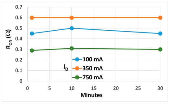
Figure 9.
Dynamic RON for a square-wave gate voltage measured at for different ID values.
It is worth noticing that the RON values are different than the ones reported in Figure 7 for the fifth pulse of the five pulses train case. In comparison to Figure 7, RON is lower (higher empty to filled traps ratio) at ID = 100 mA, almost the same at 350 mA, and higher (trapping by traps in the channel is stronger) at 750 mA. Moreover, dynamic RON values at the steady state reported in Figure 9 are at least four times higher than the DC values reported in the SGT120R65AL datasheet (0.075 Ω at low ID and VGS = 5 V). This proves that the dynamic RON is always higher than in DC, with associated switching losses that are more than expected from calculation based on DC RON values.
As a further check we measure the DC RON using a single long pulse of 30 min duration. The influence of thermal effects due to Joule heating of the drain power resistor load are minimized by mounting the resistor on a suitable heatsink. RON(t) for 100 mA and 350 mA drain current is reported in Figure 10. The trace for 100 mA is affected by noise but shows an almost zero average, the exact, very small DC RON value below the sensitivity that can be achieved by the oscilloscope. At 350 mA the average DC RON is below 0.1 Ω, a factor of six smaller than the square-wave dynamic RON value at the same drain current. This is due to an increased ratio of empty to filled traps in the channel, another evidence that electrons release increases with pulse duration.
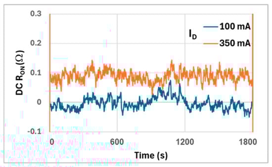
Figure 10.
DC RON vs. time for a single pulse of 30 min duration at ID = 100 mA and 350 mA.
To check whether surface/interface traps are present in the gate to drain region of the HEMT device under study, off-state DC stress tests are conducted at VDS = 55 V for 1 min, 10 min, and 30 min, with the gate terminal left floating. The small off-state leakage drain current flowing together with the high, horizontal electric field generated by VDS on the drain side of the gate can promote trapping of electrons coming in the barrier layers and interfaces in the drain access region [14]. These off-state stress tests are non-destructive and repeatable with no creation of permanent defects, such as those caused by the inverse piezoelectric effect at very high VDS when applied, even for relatively short times [15,16,17]. A subsequent single square pulse applied immediately after the stress test finds these trapped charges giving an increased and hence degraded dynamic RON.
For 1 min and 10 min off-state stress durations, no appreciable difference in dynamic RON with the pristine device is observed. On the contrary, after 30 min, the stressed device exhibits an appreciable degradation in its dynamic RON, as shown in Figure 11 for the same off-stressed and pristine (unstressed) device at a drain current of 750 mA, probed with a single pulse of 50 μs duration. It can be noted that the RON of the stressed device is about four times higher than the one of the unstressed devices. This result confirms the presence of residual surface/interface traps in the barrier layers and highlights that the adopted passivation techniques are unable to fully neutralize these traps.
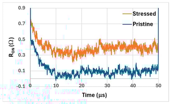
Figure 11.
Dynamic RON of the same device before (pristine) and after 30 min of off-state stress at VDS = 55 V, using a 50 µs single pulse and ID = 750 mA.
The double-pulse test (DPT) is a technique useful for testing high power switching devices driving inductive loads, as in the case where the load is made up of the windings of an electric motor. The circuit schematic for the DPT is the same as the one shown in Figure 2 but with inductive load on the drain terminal. The method has established itself as an industry standard, to the point that dedicated software programs for the oscilloscope are available to extract and measure all the switching parameters of the transistor device with a single measurement [18].
In the DPT, the gate of the HEMT is driven by two rectangular voltage pulses (0–5 V in our case) separated by an off-time interval, as shown in Figure 12a. During the first pulse, also called “storage pulse”, which is usually the longer one, the inductor is charged at constant voltage, hence, linearly increasing the current and storing magnetic energy in its internal volume. The second one is the “test pulse” and it is usually shorter than the storage pulse. The measurement and extraction of all the relevant switching parameters of the HEMT device are relative to the test pulse [19,20].
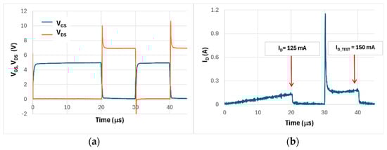
Figure 12.
Relevant voltages and drain current traces for the DPT method at nominal ID_TEST = 150 mA. (a) Double pulse of the gate voltage VGS and drain-source voltage VDS and (b) drain current ID.
In the DPT circuit schematic shown in Figure 2, the flyback power Schottky diode, connected in parallel with the inductor, reduces voltage overshoot across the inductor load during the on-to-off transitions, limiting the VDS across the switching device during the off-time and providing also a very short reverse recovery time. To prevent magnetic saturation, we use an air core inductor whose value is chosen for the desired drain current at the end of the storage pulse. The DPT measurements are conducted for drain current ID_TEST of the test pulse, ranging from 150 mA to 600 mA by changing the storage pulse duration and the drain supply voltage. The off-time and test pulse durations are both kept at 10 μs. The inductor value is accurately measured in advance as being L = 1.13 mH with an Rseries = 1.4 Ω.
The relevant traces of VGS, VDS, and ID for 20 μs storage pulse, 10 μs off-time, and 10 μs test pulse durations are reported in Figure 12. The spikes in the VDS trace are a signature of a time derivative effect due to a parasitic series capacitive coupling. The drain current in Figure 12b linearly increases with time during the storage pulse and it goes to zero during the off-time interval. At the rising edge of the subsequent test pulse there is a pronounced drain current spike. It is caused by the parasitic capacitive coupling of the current probe. These parasitic effects do not affect the accuracy of the DPT measurement, as we limit the RON extraction to the final part of the charging and test pulses.
The dynamic RON during the storage pulse, shown in Figure 13a, decreases with time, attaining a value of about 0.4 Ω at the end of the pulse. The dynamic RON for the test pulse, shown in Figure 13b, also obtains a very close value to 0.4 Ω at the end of the pulse.
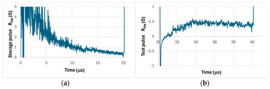
Figure 13.
RON vs. time in the DPT measurement. (a) RON during the storage pulse, (b) RON during the test pulse.
The dynamic RON vs. ID measured with the DPT method for the test pulse at 90% of its duration is compared to a 10 μs duration single-pulse measurement in Figure 14. It can be noted that the RON measured by the DPT method decreases with ID, a further proof that the ratio of trapped to free electrons in the channel becomes smaller at higher drain currents. In addition, the RON values are lower than the ones for 10 μs single rectangular pulses at the same ID (see Figure 5) because the DPT method is equivalent to the application of two VGS pulses. Only at high ID = 750 mA, where the ratio of trapped to free electrons in the channel becomes smaller, does the RON for the single pulse and DPT become quite close to each other.
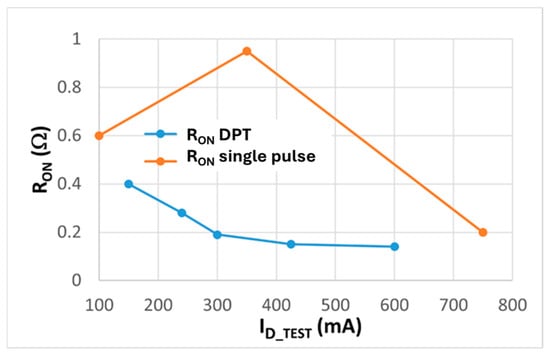
Figure 14.
Dynamic RON vs. ID measured for 10 μs test pulse of the DPT method compared to 10 μs single-pulse measurements.
4. Conclusions
Time domain measurements at relatively low ID and blocking voltage VDS allow us to study the degradation mechanisms of dynamic RON in commercial, normally off GaN on Si HEMT devices due to electron traps located in the 2DEG channel and in the buffer layer underneath. With single rectangular voltage pulses, the release of trapped electrons that is responsible for a decreased RON depends on the pulse duration as well as the drain current. At ID = 750 mA, trapping effects are dominant on a time scale below 1 μs, while for lower ID, the time scale is up to five times longer at 5 μs. Measurements of dynamic switching with a train of five pulses and a square wave show the role of cumulative effects with lower dynamic RON values as compared to the ones for single pulses. Measurements with longer pulses up to 30 min duration operate the HEMT in DC, where release mechanisms are at their maximum, giving a very low RON of about 100 mΩ at ID = 350 mA.
Devices subjected to an off-state stress test have an increased RON up to four times the one of pristine device, demonstrating the presence of surface/interface traps in the drain access region.
Finally, the values of RON measured by the DPT method show a decrease with ID with values of about 150 mΩ for currents above 350 mA, demonstrating good agreement with results from single-pulse measurements.
In summary, the presented results give useful insights into the short timescale dynamic and steady-state behavior of RON during a hard switching operation but highlight a limited device ability to maintain operational performance after prolonged off-time electrical stress. To improve the reliability and performance stability of GaN on Si HEMT devices for high-frequency and power applications, a reduction in defects and traps concentration of the GaN heterostructure, together with advanced device structures and processing techniques, is crucial and must be pursued.
Author Contributions
Conceptualization, P.C., F.V. and A.S.; methodology, P.C., F.V. and A.S.; software, F.V. and A.S.; investigation, P.C., F.V. and A.S.; writing—original draft preparation, P.C., F.V. and A.S.; writing—review and editing, P.C., F.V. and A.S.; supervision, P.C. All authors have read and agreed to the published version of the manuscript.
Funding
F. Vella and A. Sirchia acknowledge funding in the framework of the European Project “GaN4AP: GaN for Advanced Power Applications” under grant agreement No. PRJ-1035. Work carried out in the framework of the European Project “GaN4AP: Gallium Nitride for Advanced Power Applications” and the ECSEL-JU project REACTION (first and euRopEAn siC eigTh Inches pilOt liNe), Grant Agreement No. 783158.
Data Availability Statement
The original contributions presented in the study are included in the article. Further inquiries can be directed at the corresponding author.
Acknowledgments
The authors acknowledge G. Artale and A. Sferlazza for providing some of the instrumentation used for the measurements and N. Campagna for the realization of the surface mount to through hole adapter boards.
Conflicts of Interest
The authors declare no conflicts of interest.
Abbreviations
The following abbreviations are used in this manuscript:
| HEMT | High-Electron-Mobility Transistor |
| RON | Dynamic Conduction Resistance |
| DC RON | Static Conduction Resistance |
| DPT | Double-Pulse Test |
| 2DEG | Two-dimensional Electron Gas |
References
- Islam, N.; Mohamed, M.F.P.; Khan, M.F.A.J.; Falina, S.; Kawarada, H.; Syamsul, M. Reliability, Applications and Challenges of GaN HEMT Technology for Modern Power Devices: A Review. Crystals 2022, 12, 1581. [Google Scholar] [CrossRef]
- Udabe, A.; Baraia-Etxaburu, I.; Garrido Diez, D. Gallium Nitride Power Devices: A State of the Art Review. IEEE Access 2023, 11, 48628–48650. [Google Scholar] [CrossRef]
- Buffolo, M.; Favero, D.; Marcuzzi, A.; De Santi, C.; Meneghesso, G.; Zanoni, E.; Meneghini, M. Review and Outlook on GaN and SiC Power Devices: Industrial State-of-the-Art, Applications, and Perspectives. IEEE Trans. Electron. Devices 2024, 71, 1344–1355. [Google Scholar] [CrossRef]
- Scholz, F.; Bockowski, M.; Grzanka, E. GaN-Based Materials: Substrates, Metalorganic Vapor-Phase Epitaxy, and Quantum Well Properties. In Nitride Semiconductor Technology; Roccaforte, F., Leszczynski, M., Eds.; Wiley-VCH: Weinheim, Germany, 2020; pp. 41–98. [Google Scholar]
- Zhong, Y.; Zhang, J.; Wu, S.; Jia, L.; Yang, X.; Liu, Y.; Zhang, Y.; Sun, Q. A review on the GaN-on-Si power electronic devices. Fundam. Res. 2022, 2, 462–475. [Google Scholar] [CrossRef] [PubMed]
- Ajayan, J.; Kumar Panigrahy, A.; Sen, S.; Kumar, M.; Tayal, S. Reliability Issues and Degradation Mechanisms of p-GaN Gated E-Mode AlGaN/GaN Power HEMTs: A Critical Review. IEEE Access 2025, 13, 84541–84554. [Google Scholar] [CrossRef]
- Roccaforte, F.; Greco, G.; Fiorenza, P.; Iucolano, F. An Overview of Normally-Off GaN-Based High Electron Mobility Transistors. Materials 2019, 12, 1599. [Google Scholar] [CrossRef]
- Cusumano, P.; Vella, F.; Sirchia, A. Using Triangular Gate Voltage Pulses to Evaluate Hysteresis and Charge Trapping Effects in GaN on Si HEMTs. Electronics 2025, 14, 1991. [Google Scholar] [CrossRef]
- Hwang, I.; Kim, J.; Chong, S.; Choi, H.-S.; Hwang, S.-K.; Oh, J.; Shin, J.K.; Chung, U. Impact of Channel Hot Electrons on Current Collapse in AlGaN/GaN HEMTs. IEEE Electron. Device Lett. 2013, 34, 1494–1496. [Google Scholar] [CrossRef]
- Rossetto, I.; Meneghini, M.; Tajalli, A.; Dalcanale, S.; De Santi, C.; Moens, P.; Banerjee, A.; Zanoni, E.; Meneghesso, G. Evidence of Hot-Electron Effects During Hard Switching of AlGaN/GaN HEMTs. IEEE Trans. Electron. Devices 2017, 64, 3734–3739. [Google Scholar] [CrossRef]
- Tapajna, M.; Koller, C. Reliability Issues in GaN Electronic Devices. In Nitride Semiconductor Technology; Roccaforte, F., Leszczynski, M., Eds.; Wiley-VCH: Weinheim, Germany, 2020; pp. 199–241. [Google Scholar]
- Zulauf, G.; Guacci, M.; Kolar, J.W. Dynamic On-Resistance in GaN-on-Si HEMTs: Origins, Dependencies, and Future Characterization Frameworks. IEEE Trans. Power Electron. 2020, 35, 5581–5588. [Google Scholar] [CrossRef]
- Bisi, D. Characterization of Charge Trapping Phenomena in GaN-Based HEMTs. Ph.D. Thesis, University of Padua, Padua, Italy, 2015. Available online: https://www.research.unipd.it/handle/11577/3423886 (accessed on 8 June 2025).
- Tapajna, M.; Simms, R.J.T.; Pei, Y.; Kuball, M. Integrated optical and electrical analysis: Identifying location and properties of traps in AlGaN/GaN HEMTs during electrical stress. IEEE Electron. Device Lett. 2010, 31, 662–664. [Google Scholar] [CrossRef]
- Yao, Z.; Zhu, H.; Li, Y.; Xie, N.; Sun, Y.; Zhang, Y.; Liu, X.; Zhang, Z. Investigation of trap characteristics under the inverse piezoelectric effect in AlGaN/GaN HEMT devices at room temperature and low temperature. Semicond. Sci. Technol. 2023, 38, 055008. [Google Scholar] [CrossRef]
- Bisi, D.; Meneghini, M.; De Santi, C.; Chini, A.; Dammann, M.; Bruckner, P.; Mikulla, M.; Meneghesso, G.; Zanoni, E. Deep-level characterization in GaN HEMTs-Part I: Advantages and limitations of drain current transient measurements. IEEE Trans. Electron. Devices 2013, 60, 3166–3175. [Google Scholar] [CrossRef]
- Meneghini, M.; Rossetto, I.; De Santi, C.; Rampazzo, F.; Tajalli, A.; Barbato, A.; Ruzzarin, M.; Borga, M.; Canato, E.; Zanoni, E.; et al. Reliability and failure analysis in power GaN-HEMTs: An overview. In Proceedings of the IEEE International Reliability Physics Symposium (IRPS) 2017, Monterey, CA, USA, 2–6 April 2017. [Google Scholar]
- Double Pulse Testing Power Semiconductor Devices with Oscilloscope and Arbitrary Function Generator, Tektronix Appl. Note. Available online: https://www.tek.com/en/documents/application-note/double-pulse-test-tektronix-afg31000-arbitrary-function-generator (accessed on 6 June 2025).
- Wang, W.; Liang, Y.; Zhang, M.; Lin, F.; Wen, F.; Wang, H. Mechanism Analysis of Dynamic On-State Resistance Degradation for a Commercial GaN HEMT Using Double Pulse Test. Electronics 2021, 10, 1202. [Google Scholar] [CrossRef]
- Alemanno, A.; Santarelli, A.; Sangiorgi, E.; Florian, C. Characterization of the Dynamic RON of 600 V GaN Switches under Operating Conditions. Electronics 2023, 12, 943. [Google Scholar] [CrossRef]
Disclaimer/Publisher’s Note: The statements, opinions and data contained in all publications are solely those of the individual author(s) and contributor(s) and not of MDPI and/or the editor(s). MDPI and/or the editor(s) disclaim responsibility for any injury to people or property resulting from any ideas, methods, instructions or products referred to in the content. |
© 2025 by the authors. Licensee MDPI, Basel, Switzerland. This article is an open access article distributed under the terms and conditions of the Creative Commons Attribution (CC BY) license (https://creativecommons.org/licenses/by/4.0/).