Article

Comprehensive Study of Proton and Heavy Ion-Induced Damages for Cascode GaN-Based HEMTs

1
School of Optoelectronics and Communication Engineering, Xiamen University of Technology, Xiamen City 361024, China
2
Science and Technology on Reliability Physics and Application of Electronic Component Laboratory, China Electronic Product Reliability and Environmental Testing Research Institute, Guangzhou 511370, China
3
National Key Laboratory of Material Behavior and Evaluation Technology in Space Environment, Harbin Institute of Technology, Harbin 150001, China
*
Author to whom correspondence should be addressed.
Electronics 2025, 14(13), 2653; https://doi.org/10.3390/electronics14132653
Submission received: 13 May 2025 / Revised: 14 June 2025 / Accepted: 16 June 2025 / Published: 30 June 2025

Abstract

Proton and heavy ion irradiation experiments were carried out on Cascode GaN HEMT devices. Results show that device degradation from heavy ion irradiation is more significant than from proton irradiation. Under proton irradiation, obvious device degradation occurred. Low-frequency noise testing revealed a notable increase in internal defect density, reducing channel carrier concentration and mobility, and causing electrical performance degradation. Under heavy ion irradiation, devices suffered from single-event burnout (SEB) and exhibited increased leakage current. Failure analysis of post-irradiation devices showed that those with leakage current increase had conductive channels without morphological changes, while burned out devices showed obvious damage between the gate and drain regions. SRIM simulation indicated that ionization energy loss-induced electron–hole pairs and displacement damage from nuclear energy loss were the main causes of degradation. Sentaurus TCAD simulation of heavy ion irradiated GaN HEMT devices confirmed the mechanisms of leakage current increase and SEB.

1. Introduction

Gallium Nitride has several advantages compared to other semiconductor substrate, such as wide bandgap (3.39 eV), high electron mobility, high thermal conductivity, high breakdown voltage, high-temperature and high-pressure resistance, and strong radiation tolerance [1]. Based on these outstanding characteristics, Gallium Nitride based devices display great competitiveness in the field of high-frequency and high-power electronic devices [2].
In recent years, several studies have been performed on the impact of proton irradiation on GaN HEMT device performance and the single-event effects (SEEs) in GaN HEMT devices due to heavy ion irradiation. X. W. Hu et al. [3] reported that the drain saturation current of AlGaN/GaN HEMT decreased after 1.8 MeV proton irradiation when the total dose reached 1 × 1012 cm−2. D. Keum et al. [4] studied 1 MeV and 2 MeV proton irradiated AlGaN/GaN HEMT, where the drain saturation current decreased and the threshold voltage showed positive drift when the total dose reached 5 × 1014 cm−2 under 1 MeV and 2 MeV proton irradiation. L. Lv et al. [5] found that after 70 keV proton irradiation (with a total dose of 1013 cm−2), the maximum drain saturation current density and the maximum transconductance density of AlGaN/GaN MIS-HEMT decreased, and the threshold voltage increased. References [6,7,8,9] studied single-event effects in GaN HEMT using protons and reported that a significantly negative effect on the device occurs only when the total proton dose exceeds 1014 cm−2. In references [10,11,12], heavy ion irradiation was used to study the DC and RF characteristics of the devices before and after irradiation, and the results indicated that heavy ion irradiation increased the gate leakage current and source-drain leakage current of the devices.
Currently, a substantial amount of research primarily focuses on depletion-mode GaN devices and p-type gate structure enhancement-mode GaN devices subject to low-energy protons or low-energy heavy ions. However, there is a lack of reported research on the effects of high-energy protons or high-energy heavy ions on Cascode GaN HEMTs, particularly the comparative studies on the impacts of high-energy protons and high-energy heavy ions on Cascode GaN HEMTs.
In this work, proton and heavy ion irradiations were both performed on Cascode GaN HEMTs. The variations in the radiation damage induced by the two kinds of radiation sources were comparatively studied. The mechanisms of different radiation damages were analyzed based on electrical characterization and failure analysis techniques. After heavy ion irradiation, the devices were positioned using Emission Microscopy Imaging (EMMI) to locate the burnout points, and the device’s failure modes were observed using a Focused Ion Beam (FIB) microscope, and finally the Sentaurus TCAD simulation facilitating the explanations of the damage mechanism.

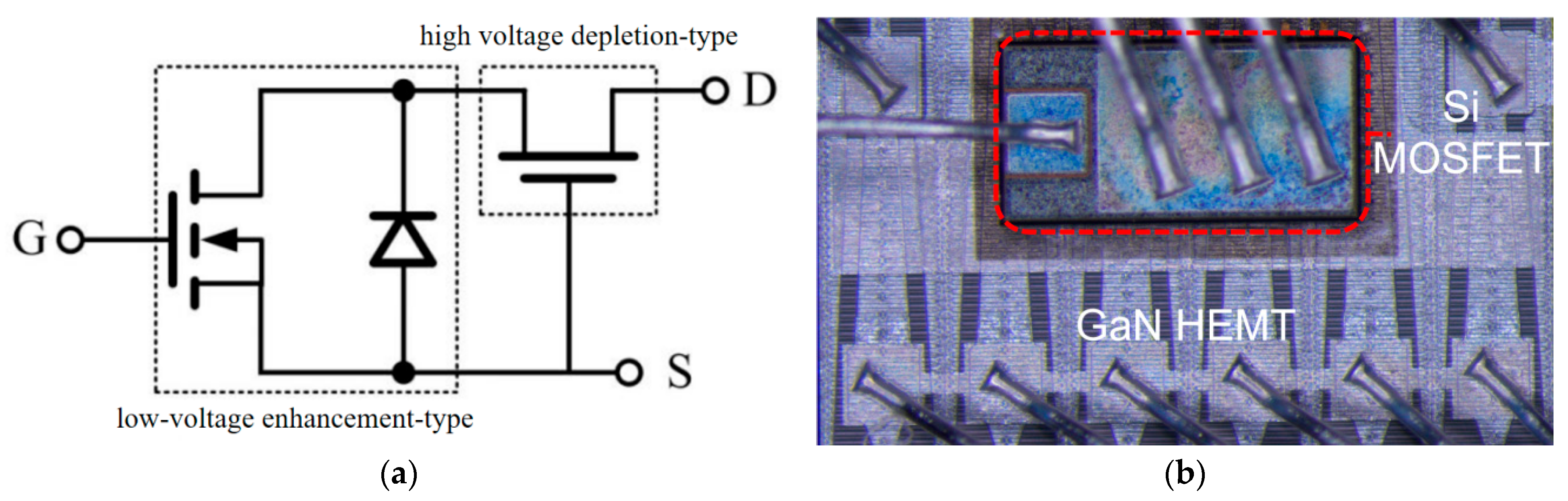
2. Samples and Experimental Setups

The devices under test (DUTs) selected in this work are normally-off cascade AlGaN/GaN HEMT devices (TP65H050WS, 650 V, 50 mΩ) from Transphorm company, Goleta, CA, USA. Figure 1 shows the Cascode device structure. It consists of a lower layer with a high-voltage depletion-mode GaN HEMT and an upper layer with a low-voltage enhancement-mode Si MOSFET, both of which are cascade-connected with a common source and gate. When the Si MOSFET is turning on, the drain-source voltage of the Si MOSFET is forward close to 0 V, at which point the gate-source voltage of the GaN HEMT is negatively close to 0 V and greater than its negative threshold voltage, enabling the GaN HEMT to conduct. When the Si MOSFET is turned off, the externally applied source-drain bias divides across the channels of the GaN HEMT and Si MOSFET, causing the normally-on GaN HEMT’s gate-source voltage to be less than its threshold voltage, thus turning it off.
The proton and heavy ion irradiation experiments were both carried out at the Space Environment Simulation and Research Infrastructure (SESRI) at Harbin Institute of Technology. This facility encompasses multiple key technologies including vacuum, cryogenics, dust particles, electromagnetic radiation, electron/proton radiation, plasma sources, weak magnetic fields, in situ or semi in situ online measurement and analysis, and life behavioral characteristic analysis. The protons had an energy level of 300 MeV, a dose rate of 2 × 108 cm−2·s−1, and a beam spot area of 1.5 × 3 cm2, resulting in a total dose of 1 × 10¹¹ p/cm2. Proton experiments were performed at room temperature with a high voltage of 650 V applied to the drain. The Keysight B1500A semiconductor parameter analyzer was employed to conduct comprehensive parameter characterization of the devices before and after irradiation. A theoretical analysis was performed on the post-irradiation variations in electrical characteristics. Subsequently, the low-frequency noise testing system was utilized to measure and analyze defects in the devices pre- and post-proton irradiation, thereby validating the conclusions derived from the semiconductor parameter analyzer. Finally, SRIM simulation software (V2013) is used to simulate the ionization and nuclear energy losses induced by 300 MeV proton irradiation into the devices with depth to analyze and verify the defect formation mechanism due to electron–hole pair excitation and displacement damage effects of proton irradiation on Si MOSFET and GaN HEMT devices.
The heavy ion irradiation used Kr ions with an energy of 500 MeV, a beam spot area of 1.5 × 3 cm2, and a total dose of 3.167 × 10⁵ p/cm2, with a linear energy transfer (LET) of 37 MeV·cm2/mg and a range of 110.61 um in GaN. The heavy ion experiment was conducted at room temperature, with three devices from the same batch subjected to different drain biases of 100 V, 150 V, and 200 V (#1 device with 100 V bias, #2 device with 150 V bias, and #3 device with 200 V bias). The output characteristics, transfer characteristics, and gate leakage current of the device were measured using the Keysight Company (Santa Rosa, CA, USA) B1500 semiconductor parameter analyzer before and after heavy ion irradiation, and the causes of the changes in electrical parameters caused by irradiation were analyzed.
After irradiation, the experimental devices underwent a decapsulation process. The decapsulated devices were used to locate the failure areas with an emission microscope (EMMI) (Advaced Company, Shanghai, China), and a focused ion beam (FIB) (ThermoFisher Company, Waltham, MA, USA) was used to spot cut and observe the device burnout. The SRIM simulation software was used to simulate the irradiation of 500 MeV Kr ions incident on Cascode GaN HEMT devices, clarifying the impacts of ionization and nuclear energy loss effects from heavy ion irradiation on the devices. Finally, the Sentaurus TCAD simulation software (V2019) was utilized to deeply reveal the microscopic physical mechanisms causing the increased leakage current and single-event burnout effect in Cascode GaN HEMT devices.

3. Results and Discussions

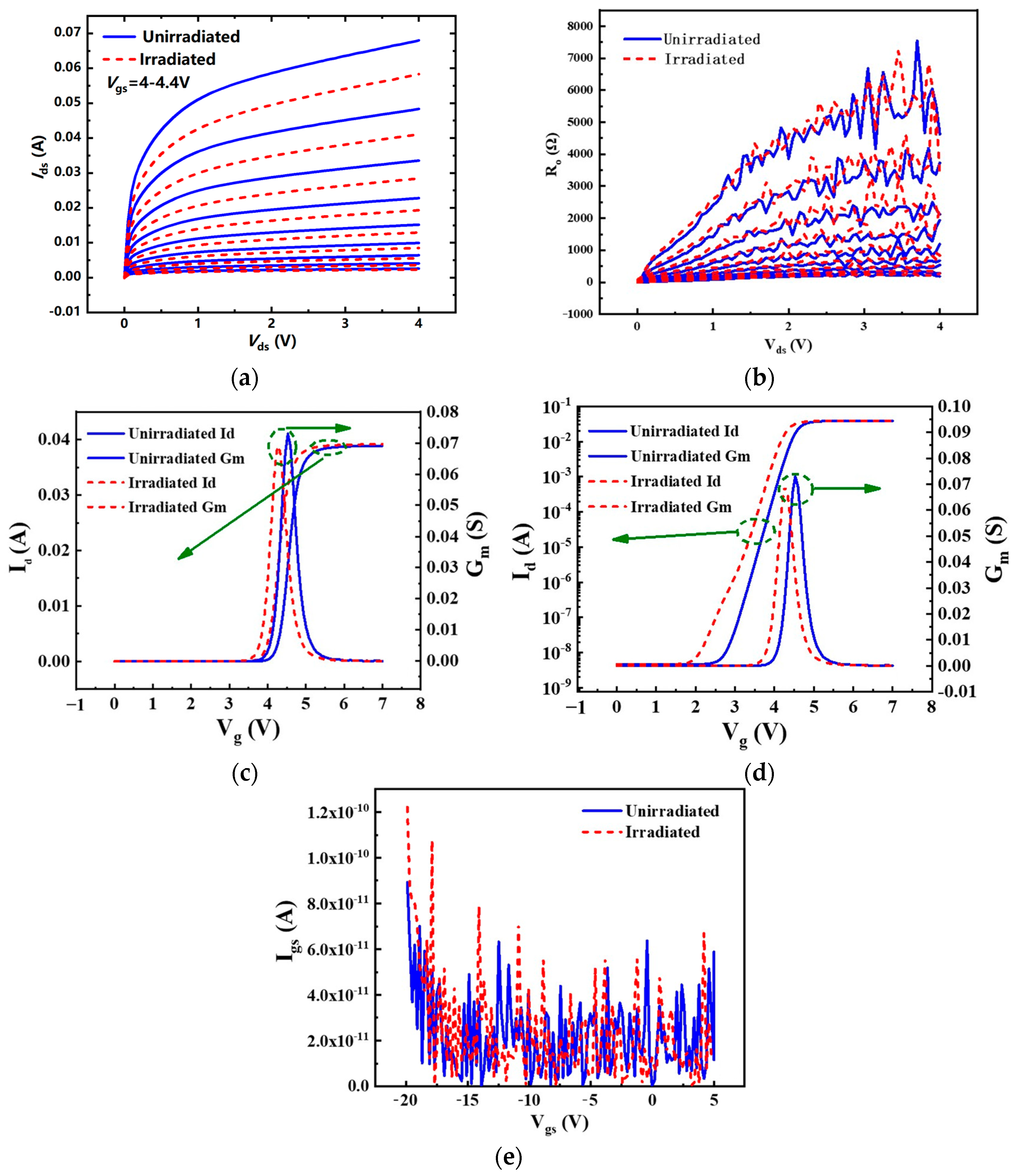
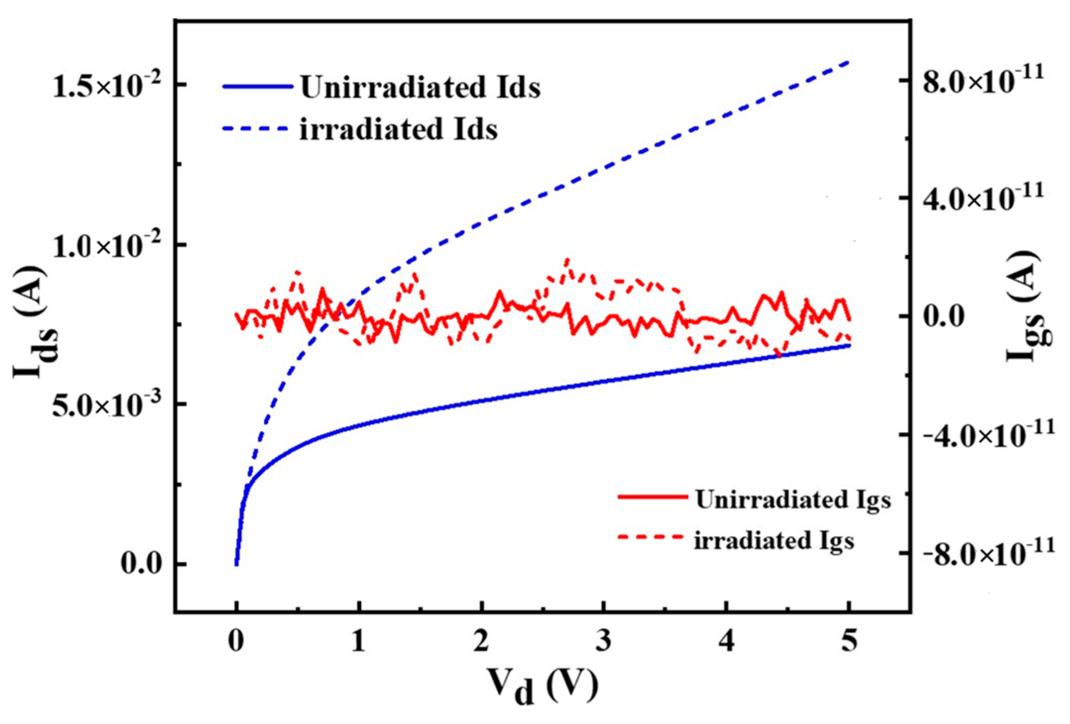
3.1. Degradation of Electrical Parameters of Devices Induced by Proton Irradiation

Electrical characterization of samples before and after proton irradiation reveals significant degradation in the electrical performance of the enhanced Cascode GaN HEMT devices. However, it is worth to note that the Cascode GaN HEMT device did not exhibit the Single Event Burnout (SEB) effect under 300 MeV proton irradiation with a drain bias of 650 V. Figure 2a depicts the output characteristics of the GaN HEMT device before and after irradiation, with configuration of Vgs = 4.0–4.4 V and a drain voltage swept of 0–4.0 V. A noticeable decrease in the saturated output current can be observed after irradiation. For instance, the maximum drain current of the device decreases by 14.23% after irradiation for the output curves at Vgs = 4.4 V. Figure 2b further illustrates the output resistance curves of the device before and after irradiation, indicating that the output resistance of the device does not change significantly after proton irradiation. Figure 2c,d show the transfer characteristics curves in linear and logarithmic scale of the device before and after irradiation, with a test condition of Vds = 0.05 V and Vgs = 0–7 V. The peak transconductance of the device decreases by 5.59% after irradiation, and the threshold voltage negatively shifts by 0.27 V. Figure 2e displays the Igs-Vgs characteristic curve before and after irradiation, showing minimal change in gate leakage current.

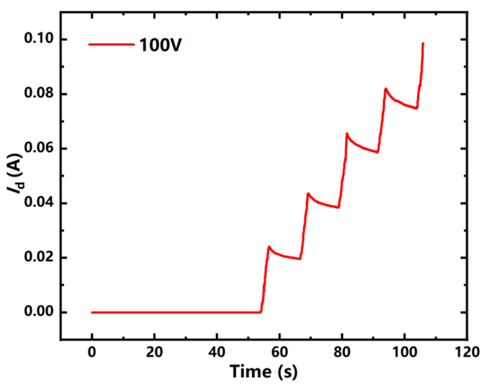
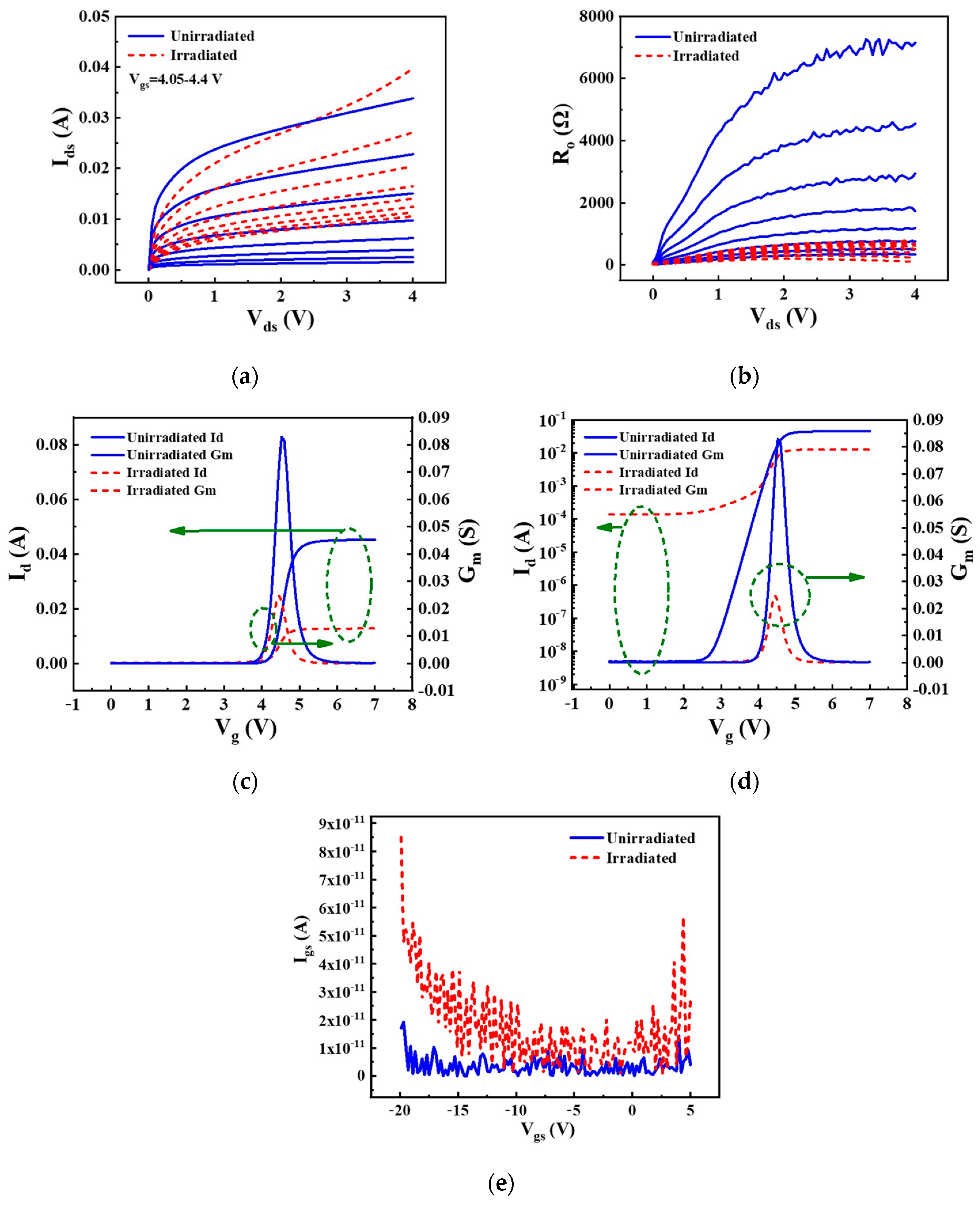
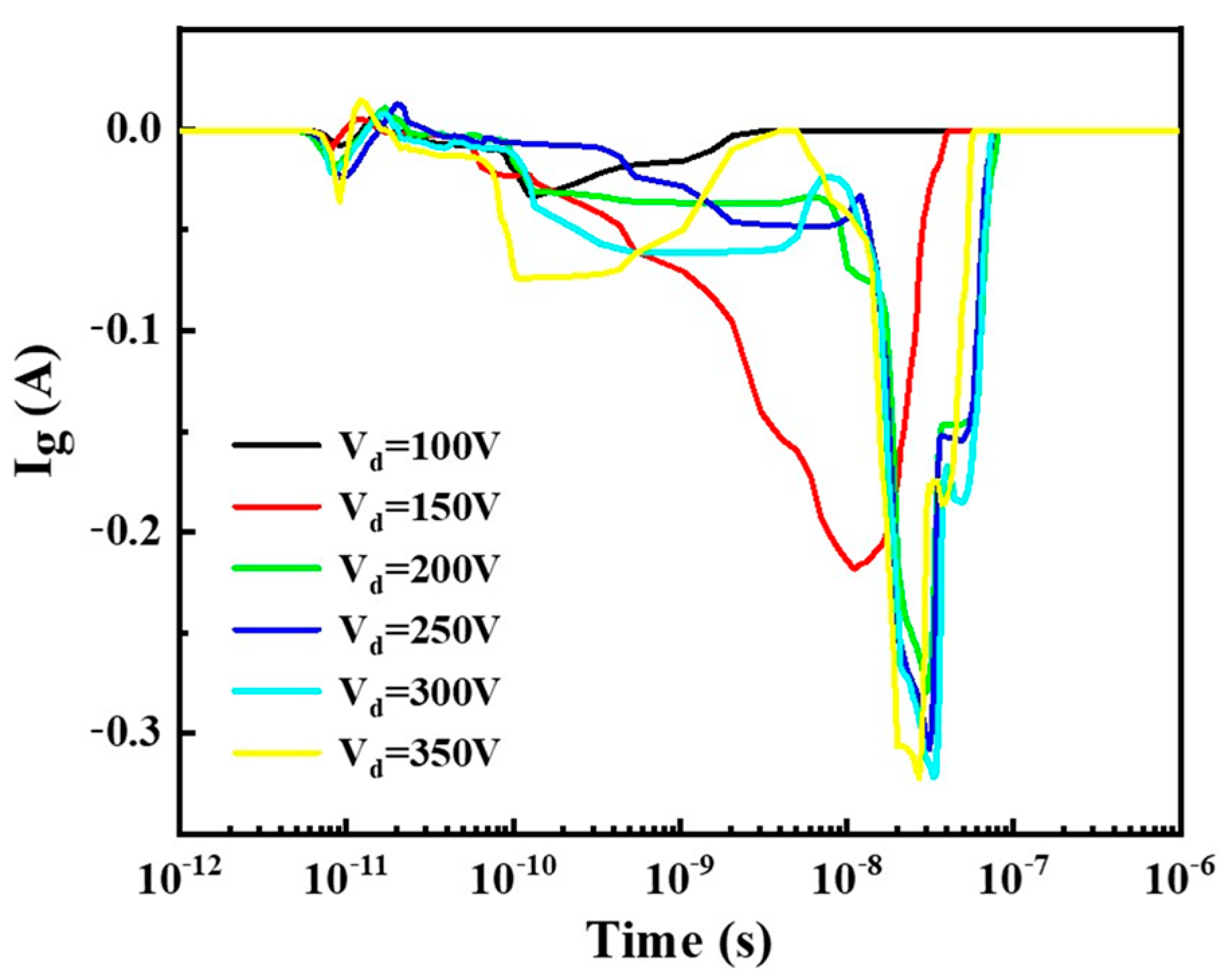
3.2. Heavy Ion Irradiation Effects

Heavy ion irradiation was conducted under three different voltage conditions. Device #1 drain biased at 100 V, #2 biased at 150 V and #3 at 200 V during irradiation. After heavy ion irradiation, device #1 exhibited a 5-order-of-magnitude increase in leakage current, and single-event burnout (SEB) occurred in devices #2 and #3. The drain current evolution with an ion energy of 500 MeV at 100 V drain bias are shown in Figure 3.
When the drain bias is set to 100 V, the drain current gradually increases with heavy ion irradiation. At a total dose of 3.167 × 10⁵ p/cm2, the current does not reach limit state, and the damage induced by the heavy ion irradiation to the device leads to a continuous increase in the drain current. Figure 4 presents the test results of device #1. In Figure 4a, the test conditions are Vgs = 4.05–4.4 V with a step size of 0.05 V, and the drain voltage varied from 0 to 4 V. Unlike proton irradiation, the output current significantly increases after irradiation. When the device is biased at Vgs = 4.05–4.4 V, the device operates in the subthreshold region. The increased output current at this bias suggests an introduction of additional leakage current paths after irradiation. Figure 4b represents the output resistance curve of the device before and after irradiation, indicating that, unlike proton irradiation, the output resistance of the device after heavy ion irradiation decreases and approaches 0, indicating serious electrical degradation or structural damage within the device. Under high-energy heavy ion irradiation, the device exhibits leakage-induced degradation. As leakage current rises with increasing irradiation dose, the device ultimately loses its reverse-blocking ability. Figure 4c,d show the transfer characteristics of the device before and after irradiation, with test conditions of Vds = 0.05 V and Vgs = 0–7 V. After irradiation, the peak transconductance of the device decreases by 70.17%, the transfer slope also decreases, and the threshold voltage negatively shifts by 0.11 V. From the logarithmic coordinate characteristics curve, it can be observed that the off-state leakage current of the device increases by five orders of magnitude after heavy ion irradiation. Figure 4e demonstrates that the reverse leakage current and forward leakage current of the device show no significant change after irradiation.
Considering the electrical characteristics before and after irradiation, the enhancement-type Cascode GaN HEMT device was more sensitive to heavy ion irradiation. Compared with the results of proton irradiation experiments shown in Figure 2, Kr ions also led to a more severe decrease in device transconductance. Moreover, the off-state leakage current of the device increased by five orders of magnitude after Kr ion irradiation.

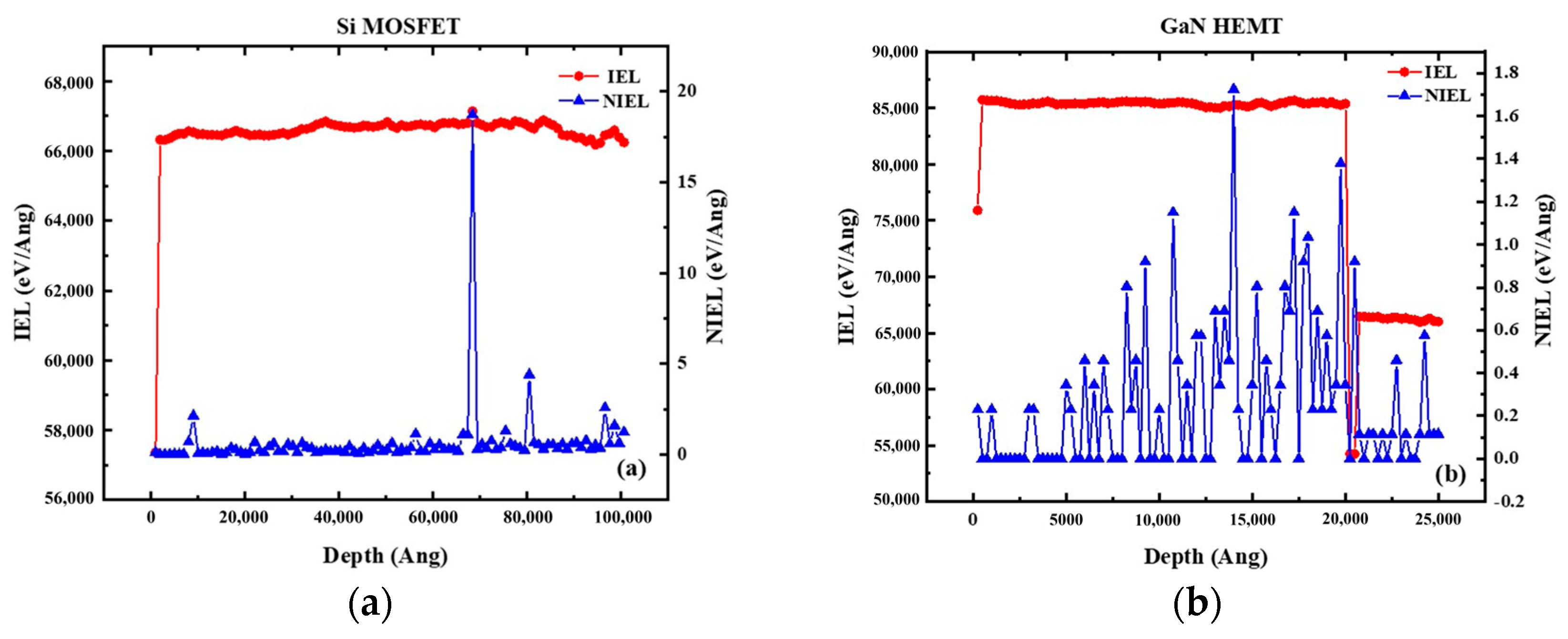
3.3. Analysis and Discussions

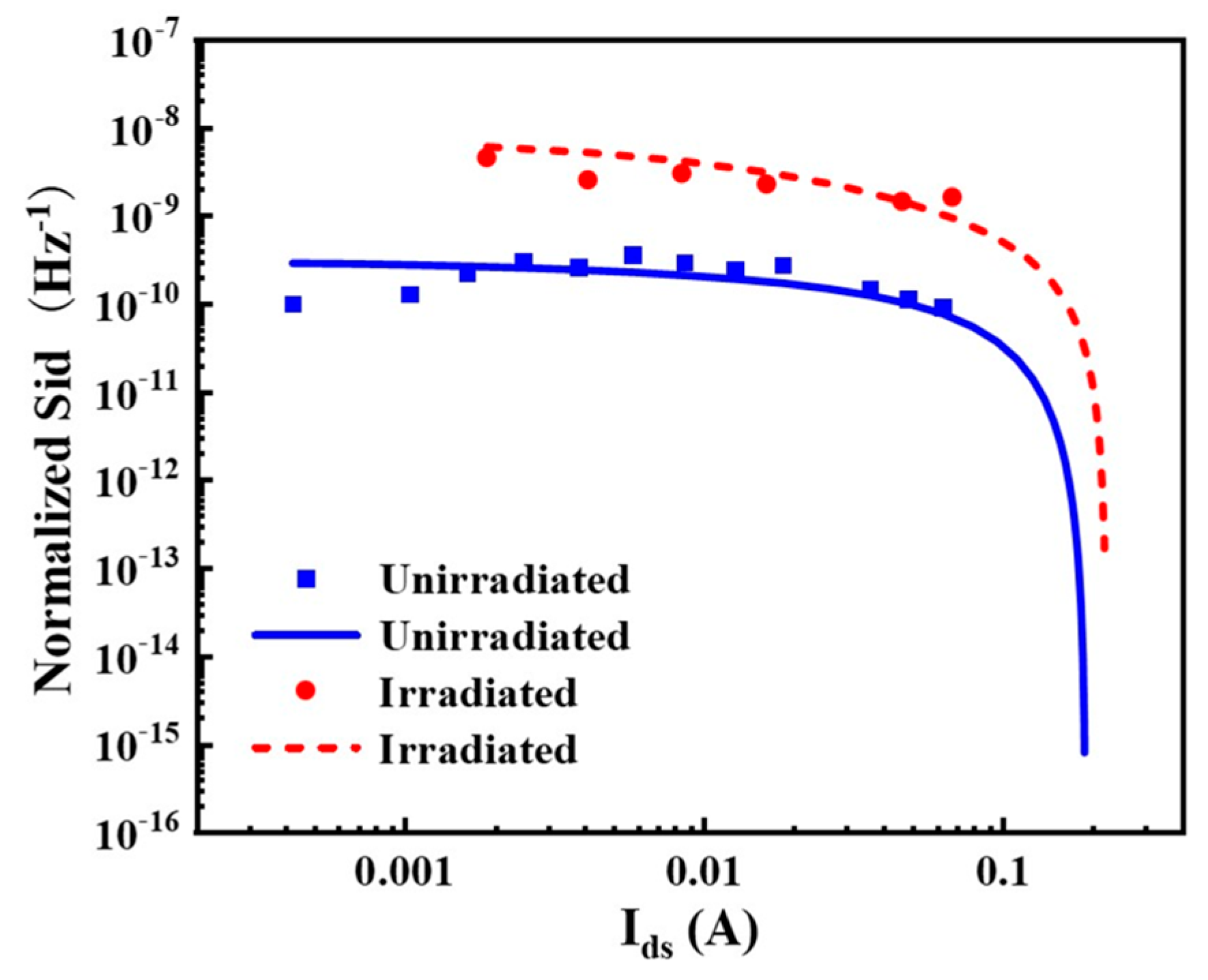
3.3.1. Characterization of Low-Frequency Noise Defects in Devices After Proton Irradiation

Through comparison and analysis of the electrical characteristics of the device before and after proton irradiation, it can be inferred that the 300 MeV proton irradiation causes an increase in internal defects of the device. These radiation-induced defects serve as generation–recombination or trapping centers for a large number of carriers, resulting in a decrease in carrier concentration and carrier mobility at the channel of the device. This ultimately leads to the degradation of electrical characteristics such as saturation output current, threshold voltage, and transconductance.
In order to further characterize the changes in defects within the GaN HEMT device before and after 300 MeV proton irradiation, the flat-band voltage noise power spectrum density (SVfb) is used to assess the device’s internal defects before and after the proton irradiation [13,14]. The relationship between the normalized channel current noise power spectrum density (Sid/Ids2) and the flat-band voltage noise power spectrum density can be expressed as follows [15]:
S id I ds 2 = ( g m I ds ) 2 S Vfb ,
S Vfb = qkT N t fWL C b 2 ( V gs - V th ) 2 · ( I ds g m ) 2 .
The parameter gm represents the transconductance of the AlGaN/GaN HEMT device, q is the elementary charge, k is Boltzmann’s constant, T is the absolute temperature, and Nt is the volume trap density (cm−3) in the gate oxide per eV. Additionally, f represents the frequency, W and L denote the width and length of the gate, respectively, Cb refers to the capacitance of the AlGaN barrier, and (Vgs-Vth) is the overdrive voltage. The magnitude of SVfb is entirely dependent on parameters such as trap charge and structural dimensions in the vicinity of the channel and is unrelated to the device’s channel current and frequency [16,17,18,19,20]. Figure 4 illustrates the functional relationship between the noise power spectral density and the drain current before and after device irradiation. Based on Equation (1), the calculated values of SVfb for the device before and after proton irradiation are 3.2205 × 10⁻¹² V2·Hz−1 and 7.9659 × 10⁻¹¹ V2·Hz−1, respectively. The relationship between defect density (Nt) and SVfb can be approximated as follows [19]:
N t = W L C b 2 f q 2 k T λ S V f b ,
λ is the conduction band alignment of the AlGaN/GaN heterojunction. As calculated in (3), after 300 MeV proton irradiation, the defect density Nt in the AlGaN/GaN device increased from 3.27 × 1016 cm−3eV−1 to 7.17 × 1016 cm−3eV−1. This indicates an increase of 3.9 × 1016 cm−3eV−1 in defect density within the device after 300 MeV proton irradiation. As can be seen from Figure 5, after proton irradiation, the defect density curve shifts upward, indicating an increase in the interface defects. This observation corroborates the aforementioned results.
The low-frequency noise testing of Cascode GaN HEMT devices measures the gate oxide layer of the cascaded Si MOSFET. Thus, threshold voltage changes are mainly influenced by Si MOSFET performance variations. From the internal equivalent circuit diagram (Figure 1) of the Cascode structure, it can be seen that the most significant feature of this device is the cascading of low-voltage enhancement Si MOSFET devices, and the overall threshold voltage of the Cascode structure is mainly controlled by the Si-based MOS tube. The mathematical model of the MOSFET threshold voltage Vth.Si is [20]
V t h . S i = q C O X ( N i t N o t ) + 4 ε S i q N A ϕ F P C O X + 2 ϕ F P + ϕ M S ,
ϕ F p = k T q l n N A N i
where Not is the oxide trap charge, Nit is the interface trap charge, Cox is the unit area gate oxide capacitance, εSi is the dielectric constant of Si, NA is the effective doping concentration in the P-type channel region, Ni is the intrinsic carrier concentration in silicon, ΦFP is the Fermi potential of P-type substrate, and ΦMS is the metal-semiconductor work function difference. The negative drift of Vth is mainly caused by electron–hole pairs induced by proton irradiation in the gate oxide layer. Due to the higher electron mobility in the oxide layer compared to holes, electrons can leave the gate oxide layer in a relatively short time. When most of the holes move toward the SiO2/Si interface, they are captured by traps to form Not and Nit. Since oxide traps capture charges more easily than interface traps, Not increases much more than Nit, causing Vth.Si to decrease. Vth of the cascade device is directly related to the Vth.Si of the MOSFET device, so a decrease in Vth. When the Cascode device operates in the saturation region, the source-drain output current, IDS, is mainly limited by the Ids.Si of the Si MOSFET, and thus IDS is forced to limit as Ids.Si decreases [21].
The SRIM software was employed to simulate the ionization energy loss distribution of 300 MeV proton irradiation on Cascode GaN HEMT devices, which generates numerous electron–hole pairs. The nuclear energy loss distribution was also examined to reveal the displacement damage effects caused by proton irradiation, thereby explaining the proton irradiation damage mechanism. The simulation results are shown in Figure 6. Figure 6a presents the depth-dependent variations in ionization energy loss and nuclear energy loss in the enhancement-mode Si MOSFET device, while Figure 6b displays the corresponding depth-dependent variations in ionization energy loss and nuclear energy loss in the depletion-mode GaN HEMT device. The ionization energy of Si is 3.6 eV, and that of GaN is 8.9 eV, which is the energy needed to form an electron–hole pair upon irradiation. This suggests that GaN HEMT devices have better resistance to ionization-induced damage than Si MOSFET devices. As shown in Figure 6, after 300 MeV proton irradiation, ionization energy loss occurs in the devices. In the Si MOSFET, the ionization energy loss at the SiO2/Si interface is 6.632 × 10⁴ eV/Å, while in the GaN HEMT, the corresponding value at the AlGaN/GaN interface is 8.572 × 10⁴ eV/Å. Analysis shows that proton irradiation causes more severe ionization damage in Si MOSFET devices. This generates a large number of electron–hole pairs, which in turn affect the electrical performance of the device.
It can also be seen from Figure 6 that nuclear energy loss occurs in the device under proton irradiation, indicating that displacement damage effects have taken place. The nuclear energy loss in Si MOSFET devices is higher than that in GaN HEMT devices. The displacement damage caused by nuclear energy loss creates numerous defects in the material, which ultimately leads to the degradation of the device’s electrical properties. This is consistent with the above LFN experimental results. The SRIM software calculates that the energy required to form a vacancy in Si is 2.333 eV/Vacancy and in GaN is 2.875 eV/Vacancy. This shows that under proton irradiation, Si MOSFET devices are more susceptible to displacement damage and trap charge formation. As a result, their post-irradiation degradation is more pronounced. Therefore, the degradation of Cascode GaN HEMT devices under proton irradiation is mainly due to the influence of Si MOSFET devices. Although GaN HEMTs are also affected by irradiation, the impact is relatively small.

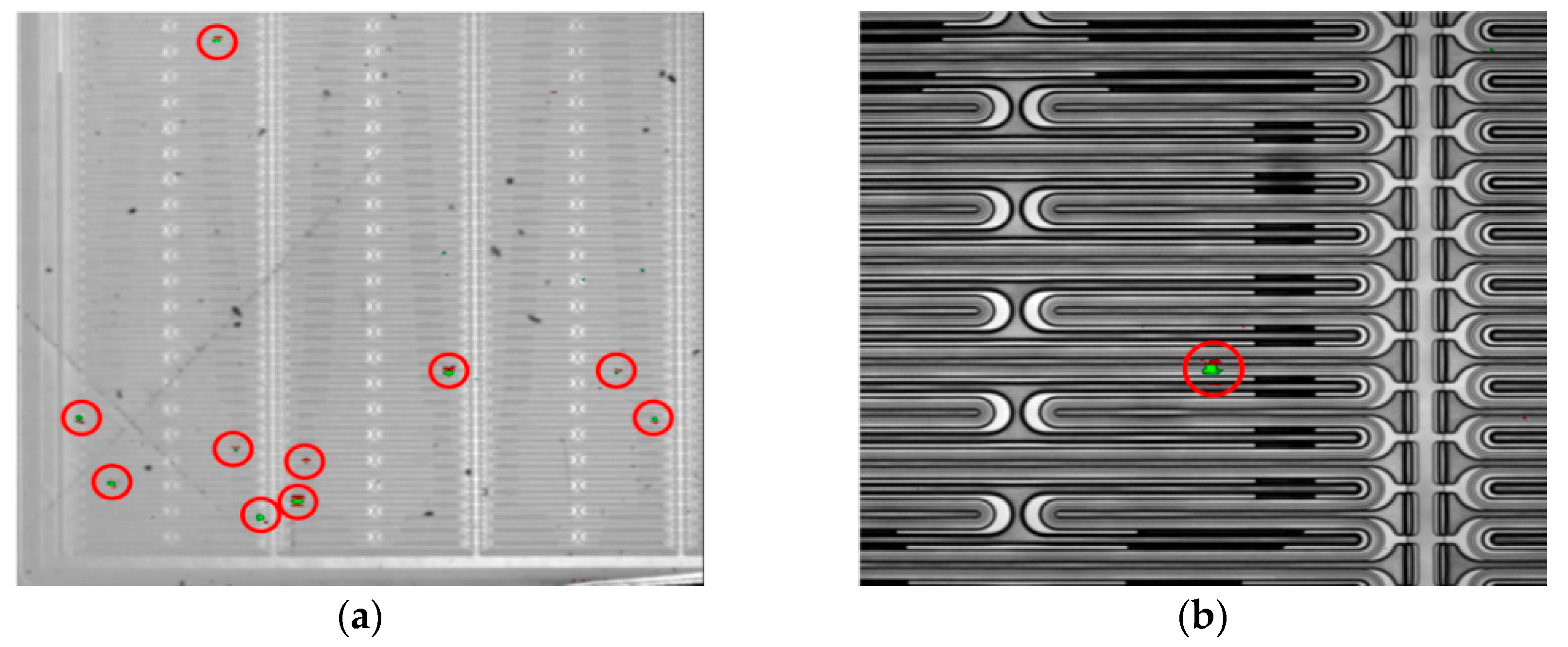
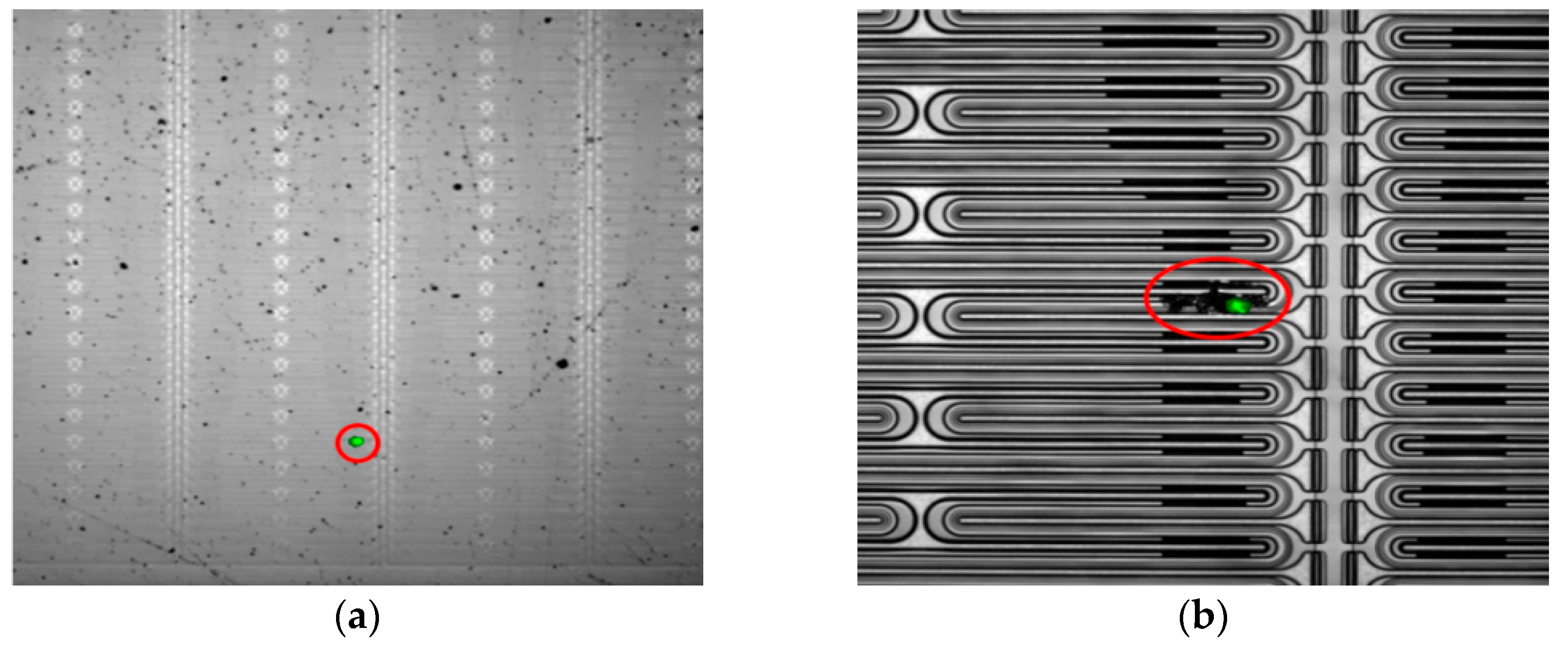
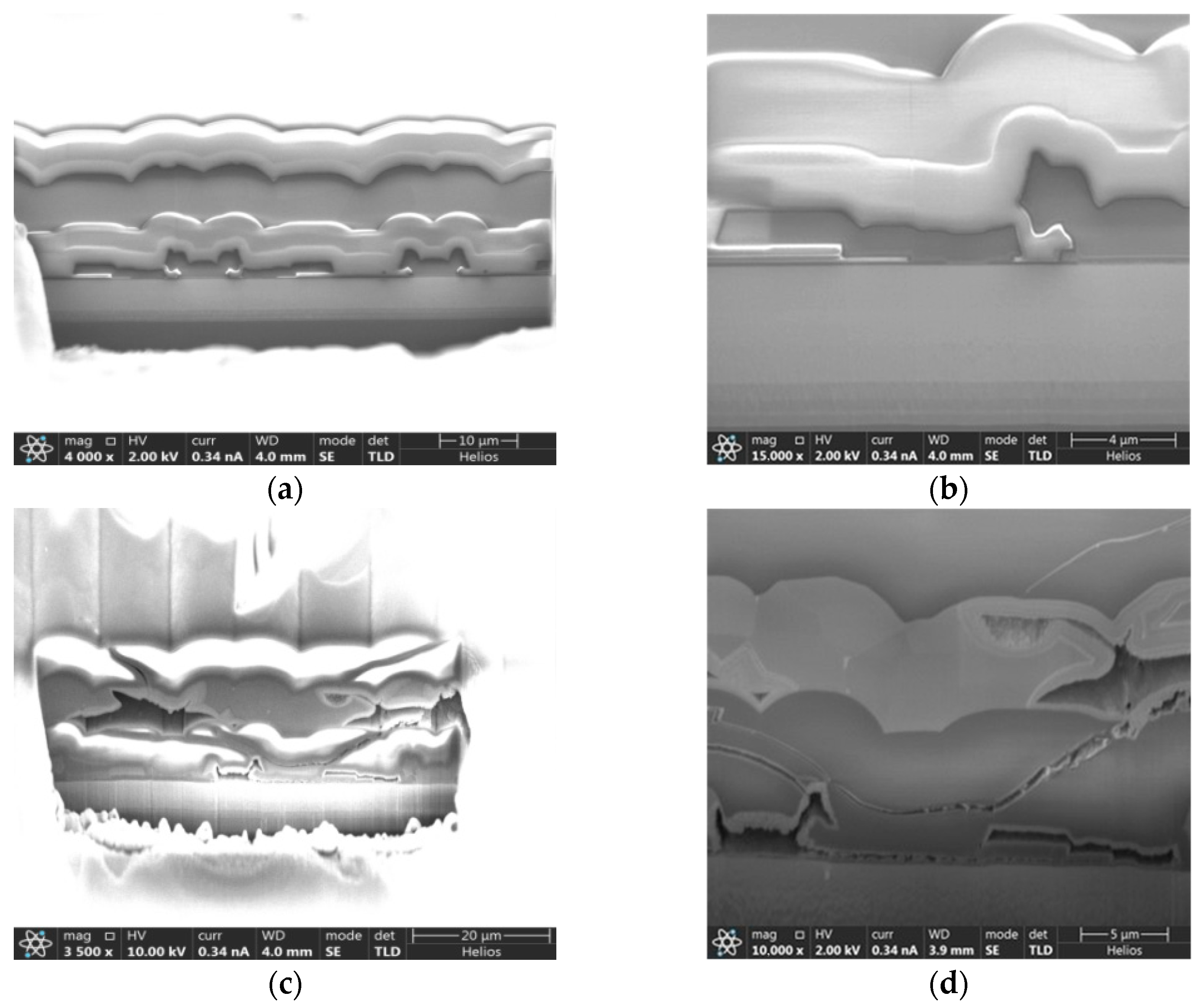
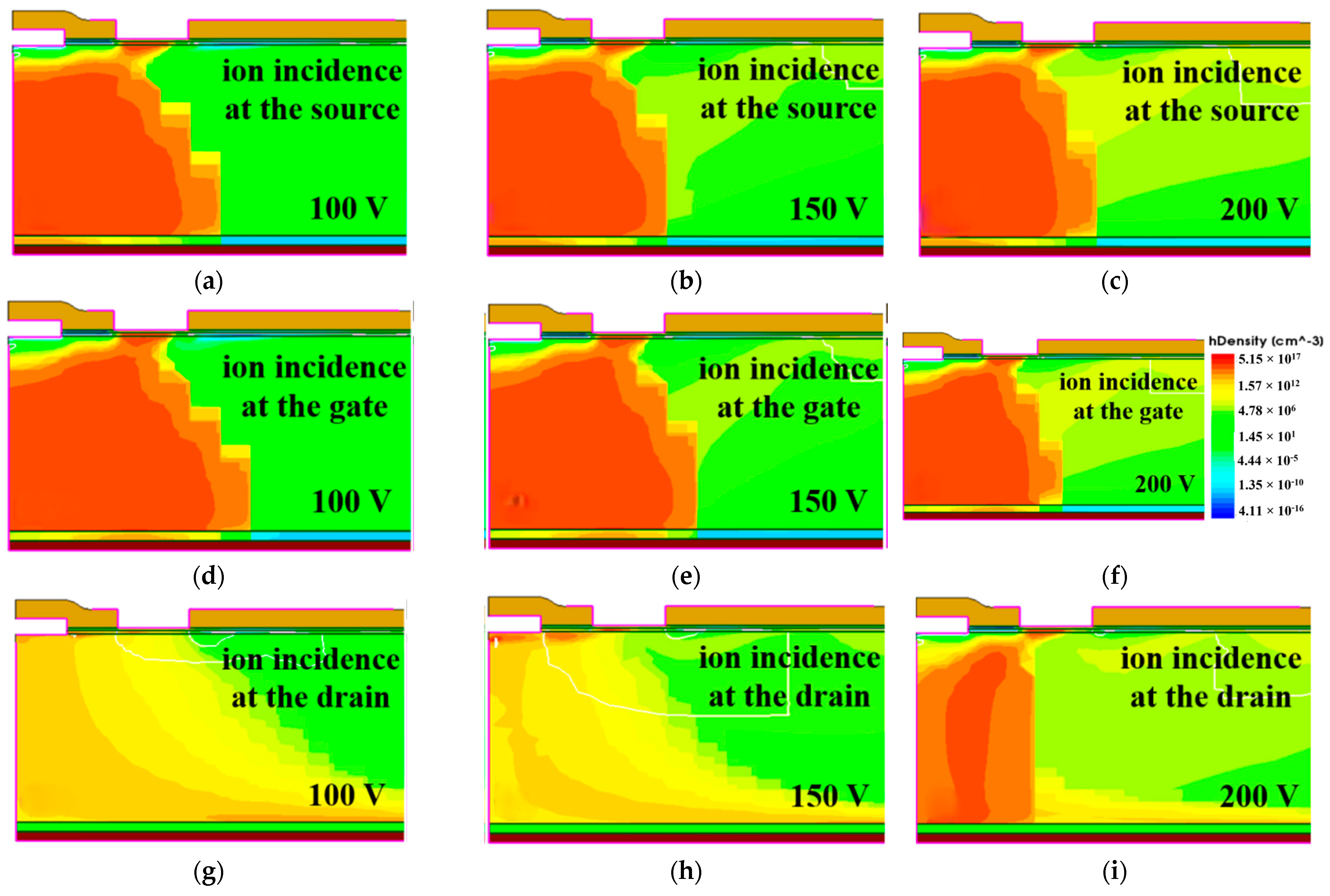
3.3.2. Failure Analysis of Devices After Heavy Ion Irradiation

Compared to proton irradiation, Kr ion irradiation leads to a more severe reduction in transconductance. Furthermore, there is a five-orders-of-magnitude increase in off-state leakage current. From the analysis of the output characteristic curve in Figure 4a, it can be observed that the output current of the device decreased after proton irradiation compared to before irradiation, whereas the device irradiated with heavy ions exhibits an increasing trend. This is due to the increase in off-state leakage current that causes the output leakage current to rise in the heavy ion irradiated device when it is not fully turned on. That is, it indicates the presence of conductive channels between the source-drain regions of the device.
Considering that the metal wiring at the front side of GaN HEMT might cover the light emission, the EMMI analysis was conducted from the back side with the back metal stripped by grinding. The #1 device was opened, and an emission microscope (EMMI) was used to detect photons emitted and locate the fault points as shown in Figure 7. Multiple failure points distributed in different locations were found on the depletion GaN, while the enhancement Si MOSFET did not have any fault points. Each fault point represents a conductive channel and contributes to the increase in leakage current after heavy ion irradiation. The microscope was used to capture detailed images of the fault area of the device. It can be seen from Figure 7b that no significant material damage or morphological changes were observed at the failure location. Figure 8 presents the test results of the EMMI for device #2. It shows that the depletion-mode GaN HEMT device within the Cascode structure exhibits a Single Event Burnout (SEB) phenomenon, primarily occurring in the metal interconnect layer. The extracted details of the device fault points from Figure 8b reveal a significant burnout phenomenon between the gate and drain regions.
Using EMMI for fault localization, targeted cutting of the burnt points was performed using focused ion beam microscopy (FIB) to observe the sectioned burnt points of the device. A comparison between Figure 9 indicates that there exists a void burnt between the gate and drain regions of the #2 device. The cross-sectional image cut by FIB in Figure 9c,d reveals that the internal metal of the device has been burned into a void due to the SEB effect.
Figure 10 illustrates the gate and drain current characteristics of the Cascode device as a function of drain voltage (Vd) at a gate voltage (Vg) of 4.2 V under off-state conditions after heavy ion irradiation. It can be observed that the gate current remains at the nA level before and after irradiation, indicating that the gate-source region is in the off state. However, the drain current increases with increasing drain voltage, suggesting the presence of a conductive channel between the source and drain regions. Further analysis suggests that the weakened Schottky barrier leads to a decrease in gate controllability, resulting in increased leakage current. When the leakage current becomes sufficiently large, a conductive channel forms between the source and drain.Based on the analysis of the internal circuit structure of the cascaded GaN device shown in Figure 1, it is evident that the TP65H050WS GaN device consists of a low-voltage enhancement-mode Si MOSFET and a high-voltage depletion-mode GaN HEMT connected in a common source and common gate configuration. When the device is in the reverse-biased cutoff state, the low-voltage enhancement-mode Si MOSFET is cutoff. The drain of the high-voltage depletion-mode GaN HEMT, the gate of the GaN HEMT, and the source of the Si MOSFET can form a leakage path between the source and drain, leading to high current phenomena at the source-drain terminals of the device. This is likely the primary reason for the SEB region in the high-voltage depletion-mode GaN HEMT observed in Figure 8 [22,23].
To deeply explore the failure mechanisms of Cascode GaN HEMTs caused by Kr ions, 2D device simulations were conducted using the Sentaurus TCAD. The models used included carrier statistical, hot electron emission, heterojunction, carrier mobility, generation–recombination, piezoelectric polarization, tunneling, and heavy ion effects models. During simulation, the GaN HEMT was set to the off-state, with radiation particles vertically incident from the gate-drain region. To match the irradiation experiment, the ion LET value was set to 0.543 pC/μm (about 37 MeV·cm2/mg for GaN). The ion penetration depth was 3 μm to cover the entire device. The ion-induced failure factors in the device were examined by varying the drain bias [24].
Based on the aforementioned model, heavy ion irradiation simulation experiments were conducted on depletion-mode GaN HEMTs. The simulation structure diagram of the device is shown in Figure 11. From top to bottom: metal contact layer, silicon oxide passivation layer, AlGaN barrier layer, GaN channel layer, GaN or AlGaN buffer layer (Al composition of 0.02), AlN seed layer, and oxide layer. From left to right: source, gate, drain. Relevant parameters are listed in Table 1. Although discrepancies exist between the simulation device data/structure and the experimental device structure, the conclusions drawn through qualitative analysis suffice to provide theoretical guidance for this study.
Figure 12 presents the drain transient current variations in GaN HEMT devices caused by radiation ion incidence at different drain biases. As shown in Figure 12, at a drain bias of 100 V, the device’s drain transient current variation is insignificant, and no SEB occurs. However, when the drain bias ranges from 150 V to 350 V, the drain current surges, exceeding 1 A. The resulting transient temperature rise causes thermal damage, leading to SEB in the device.
Figure 13 presents the gate transient current variations in GaN HEMT devices caused by radiation ion incidence at different drain biases. As shown in Figure 13, as the drain bias and particle irradiation time increase, the gate current rises and then drops to 0 A. This is because heavy ion incidence generates numerous electron–hole pairs. Electrons move towards the drain and are collected, while holes migrate towards the gate and accumulate. The accumulated holes in the AlGaN layer at the Schottky interface form a positive charge region, counteracting the electrons on the metal side and weakening the Schottky barrier.
Figure 14 shows that regardless of the incidence angle of heavy ions, numerous holes gather below the gate. As the drain bias increases, more holes are driven towards the gate by the electric field, leading to hole accumulation at the gate. These holes are captured by defects at the interface caused by irradiation, forming a local positive charge layer. This partially offsets the intrinsic polarization-induced negative charge in the AlGaN layer, weakening the polarization electric field and narrowing the depletion region. The narrowed depletion region reduces the band bending of the Schottky barrier, lowering the barrier height. The reduced Schottky barrier allows more electrons to tunnel through, increasing leakage current. At higher drain biases, as shown in Figure 12, local transient large currents occur and persist for a while, gradually increasing the maximum lattice temperature within the device, causing thermal damage and SEB. As a conclusion, the degradation mechanisms observed in this study are compared to similar studies conducted on other semiconductor devices under radiation, as shown in Table 2.

4. Conclusions

Proton and heavy ion irradiation experiments were carried out on Cascode GaN HEMT devices. Results show that under 650 V drain bias, proton irradiation degrades the device’s electrical characteristics without causing single-event burnout (SEB). Under 100 V drain bias, heavy ion irradiation significantly alters electrical properties, increasing the off-state drain current by five orders of magnitude. At 150 or 200 V drain bias, heavy ion irradiation induces SEB. Post-irradiation failure analysis and simulation results indicate that the electrical degradation after proton and heavy ion irradiation is due to the combined effects of ionization energy loss-generated electron–hole pairs and displacement damage caused by nuclear energy loss. The increased leakage current and SEB after heavy ion irradiation are attributed to a weakened Schottky barrier.

Author Contributions

Conceptualization, X.W. and J.Y.; methodology, Z.L.; formal analysis, Z.W.; investigation, C.P.; resources, X.C.; data curation, T.M.; writing—original draft preparation, Z.Z.; writing—review and editing, H.H. and H.S.; supervision, Y.H.; project administration, Y.C.; funding acquisition, G.L. All authors have read and agreed to the published version of the manuscript.

Funding

This research was funded by National Natural Science Foundation of China, grant number 12375268 and 12075065 and Foundation of National Key Laboratory of Materials Behavior and Evaluation Technology in Space Environment, grant number 6142910220209.

Data Availability Statement

The data presented in this study are available on request from the corresponding author due to privacy.

Conflicts of Interest

The authors declare no conflicts of interest. The funders had no role in the design of the study; in the collection, analyses, or interpretation of data; in the writing of the manuscript; or in the decision to publish the results.

References

  1. Shen, L.; Heikman, S.; Moran, B.; Coffie, R.; Zhang, N.-Q.; Buttari, D.; Smorchkova, I.; Keller, S.; DenBaars, S.; Mishra, U. AlGaN/AlN/GaN high-power microwave HEMT. IEEE Electron Device Lett. 2001, 22, 457–459. [Google Scholar] [CrossRef]
  2. Ambacher, O.; Smart, J.; Shealy, J.R.; Weimann, N.G.; Chu, K.; Murphy, M.; Schaff, W.J.; Eastman, L.F.; Dimitrov, R.; Wittmer, L.; et al. Two-dimensional electron gases induced by spontaneous and piezoelectric polarization charges in N-and Ga-face AlGaN/GaN heterostructures. J. Appl. Phys. 1999, 85, 3222–3233. [Google Scholar] [CrossRef]
  3. Hu, X.; Choi, B.; Barnaby, H.; Fleetwood, D.; Schrimpf, R.; Lee, S.; Shojah-Ardalan, S.; Wilkins, R.; Mishra, U.; Dettmer, R. The energy dependence of proton-induced degradation in AlGaN/GaN high electron mobility transistors. IEEE Trans. Nucl. Sci. 2004, 51, 293–297. [Google Scholar] [CrossRef]
  4. Keum, D.; Kim, H. Energy-dependent degradation characteristics of AlGaN/GaN MISHEMTs with 1, 1.5, and 2 MeV proton irradiation. ECS J. Solid State Sci. Technol. 2018, 7, Q159–Q163. [Google Scholar] [CrossRef]
  5. Lv, L.; Lin, Z.; Guo, H.; Pan, X.; Yan, X. Proton irradiation effects on enhancement-mode AlGaN/GaN MIS-HEMTs devices. Mod. Appl. Phys. 2021, 12, 86–92. [Google Scholar]
  6. Puzyrev, Y.S.; Roy, T.; Zhang, E.X.; Fleetwood, D.M.; Schrimpf, R.D.; Pantelides, S.T. Radiation-induced defect evolution and electrical degradation of AlGaN/GaN high-electron-mobility transistors. IEEE Trans. Nucl. Sci. 2011, 58, 2918–2924. [Google Scholar] [CrossRef]
  7. Anderson, T.J.; Koehler, A.D.; Specht, P.; Weaver, B.D.; Greenlee, J.D.; Tadjer, M.J.; Hite, J.K.; A Mastro, M.; Porter, M.; Wade, M.; et al. Failure mechanisms in AlGaN/GaN HEMTs irradiated with 2 MeV protons. ECS Trans. 2015, 66, 15–20. [Google Scholar] [CrossRef]
  8. Lv, L.; Ma, X.; Zhang, J.; Bi, Z.; Liu, L.; Shan, H.; Hao, Y. Proton irradiation effects on AlGaN/AlN/GaN heterojunctions. IEEE Trans. Nucl. Sci. 2015, 62, 300–305. [Google Scholar] [CrossRef]
  9. Koehler, A.D.; Anderson, T.J.; Khachatrian, A.; Roche, N.J.-H.; Buchner, S.; Weaver, B.D.; Hobart, K.D.; Kub, F.J. Displacement damage and single event effects in AlGaN/GaN HEMTs. ECS Trans. 2017, 75, 13–20. [Google Scholar] [CrossRef]
  10. Rostewitz, M.; Hirche, K.; Latti, J.; Jutzi, E. Single event effect analysis on DC and RF operated AlGaN/GaN HEMTs. IEEE Trans. Nucl. Sci. 2013, 60, 2525–2529. [Google Scholar] [CrossRef]
  11. Poling, B.S.; Via, G.D.; Bole, K.D.; Johnson, E.E.; McDermott, J.M. Commercial-off the-shelf AlGaN/GaN HEMT device reliability study after exposure to heavy ion radiation. Microelectron. Reliab. 2017, 68, 13–20. [Google Scholar] [CrossRef]
  12. Lei, Z.-F.; Guo, H.-X.; Zeng, C.; Chen, H.; Wang, Y.-S.; Zhang, Z.-G. Influence of heavy ion irradiation on DC and gate-lag performance of AlGaN/GaN HEMTs. Chin. Phys. B 2015, 24, 056103. [Google Scholar] [CrossRef]
  13. Liu, Y.; Chen, H.B.; He, Y.J.; Wang, X.; Yue, L.; En, Y.F.; Liu, M.H. Radiation effects on the low frequency noise in partially depleted silicon on insulator transistors. Acta Phys. Sin. 2015, 64, 078501. [Google Scholar]
  14. Christensson, S.; Lundström, I.; Svensson, C. Low frequency noise in MOS transistors-I theory. Solid State Electron. 1968, 11, 797–812. [Google Scholar] [CrossRef]
  15. Chen, Y.Q.; Zhang, Y.C.; Liu, Y.; Liao, X.Y.; En, Y.F.; Fang, W.X.; Huang, Y. Effect of hydrogen on defects of AlGaN/GaN HEMTs characterized by low-frequency noise. IEEE Trans. Electron Devices 2018, 65, 1321–1326. [Google Scholar] [CrossRef]
  16. Yue, S.; Lei, Z.; Peng, C.; Zhong, X.; Wang, J.; Zhang, Z.; En, Y.; Wang, Y.; Hu, L. High-fluence proton-induced degradation on AlGaN/GaN high-electron-mobility transistors. IEEE Trans. Nucl. Sci. 2020, 67, 1339–1344. [Google Scholar] [CrossRef]
  17. Koehler, A.D.; Hobart, K.D.; Weatherford, T.R.; Kub, F.J.; Specht, P.; Anderson, T.J.; Weaver, B.D.; Greenlee, J.D.; Tadjer, M.J.; Porter, M.; et al. Proton radiation-induced void formation in Ni/Au-Gated AlGaN/GaN HEMTS. IEEE Electron Device Lett. 2014, 35, 1194–1196. [Google Scholar] [CrossRef]
  18. Chen, Z.; Yue, S.; Wang, J.; Zhang, Z.; Huang, Y.; Wang, L.; Peng, C.; Zhong, X.; Lei, Z. Proton-induced effect on AlGaN/GaN HEMTs after hydrogen treatment. IEEE Trans. Device Mater. Reliab. 2021, 21, 297–302. [Google Scholar] [CrossRef]
  19. Silvestri, M.; Uren, M.J.; Killat, N.; Marcon, D.; Kuball, M. Localization of off-stress-induced damage in AlGaN/GaN high electron mobility transistors by means of low frequency 1/f noise measurements. IEEE Trans. Electron Devices 2013, 103, 043506. [Google Scholar] [CrossRef]
  20. Bai, R.; Guo, H.; Zhang, H.; Wang, D.; Zhang, F.; Pan, X.; Ma, W.; Hu, J.; Liu, Y.; Yang, Y.; et al. Study of high-energy proton radiation effects in GaN power devices with enhanced Cascode structure. Acta Phys. Sin. 2023, 72, 63–69. [Google Scholar] [CrossRef]
  21. Huang, Y. Investigation of the mechanism of weak radiation-induced failure in GaN-based Cascode-type devices. China Integr. Circuits 2023, 32, 62–66. [Google Scholar]
  22. Chen, R.; Liang, Y.; Han, J.; Wang, X.; Yang, H.; Chen, Q.; Yuan, R.; Ma, Y.; Shangguan, S. Experimental study on single-event and total-dose effects of gallium nitride-based high electron mobility transistors. Acta Phys. Sin. 2021, 70, 252–259. [Google Scholar]
  23. Wan, P.; Yang, J.; Ying, T.; Lv, G.; Lva, L.; Dong, S.; Dongb, L.; Yu, X.; Zhen, Z.; Li, W.; et al. Effects of Ionization and Displacement Damage in AlGaN/GaN HEMTs Devices Caused by Various Heavy Ions. IEEE Trans. Nucl. Sci. 2021, 68, 1265–1271. [Google Scholar] [CrossRef]
  24. Peng, C.; Lei, Z.; Zhang, Z.; He, Y.; Chen, Y.; Lu, G.; Huang, Y. Mechanism of SiC Schottky barrier diode damage due to heavy ion irradiation. Acta Phys. Sin. 2022, 71, 176101. [Google Scholar] [CrossRef]
  25. Witulski, A.F.; Arslanbekov, R.; Raman, A.; Schrimpf, R.D.; Sternberg, A.L.; Galloway, K.F.; Javanainen, A.; Grider, D.; Lichtenwalner, D.J.; Hull, B. Single-Event Burnout of SiC Junction Barrier Schottky Diode High-Voltage Power Devices. IEEE Trans. Nucl. Sci. 2018, 65, 256–261. [Google Scholar] [CrossRef]
  26. Ma, Y.; Gao, B.; Gong, M.; Willis, M.; Yang, Z.; Guan, M.; Li, Y. High fluence swift heavy ion structure modification of the SiO2/Si interface and gate insulator in 65nm MOSFETs. Nucl. Instrum. Methods Phys. Res. Sect. B Beam Interact. Mater. At. 2017, 396, 56–60. [Google Scholar] [CrossRef]
  27. Chen, R.; Liang, Y.-N.; Han, J.-W.; Wang, X.; Yang, H.; Chen, Q.; Yuan, R.-J.; Ma, Y.-Q.; Shangguan, S.-P. Single event effect and total dose effect of GaN high electron mobility transistor using heavy ions and gamma rays. Acta Phys. Sin. 2021, 70, 116102-1–116102-8. [Google Scholar] [CrossRef]
  28. Li, X.; Jiang, W.; Wang, Y.; Zhang, H.; Peng, C.; Zhang, X.; Liang, X.; Fu, W.; Zhang, Z.; Lei, Z.; et al. Single-event burnout in β-Ga2O3 Schottky barrier diode induced by high-energy proton. Appl. Phys. Lett. 2024, 125, 092101. [Google Scholar] [CrossRef]
Figure 1. Cascode device structure. (a) Equivalent schematic; (b) physical diagram of the device.
Electronics 14 02653 g001
Figure 2. Electrical characteristic curves of Cascode GaN HEMTs under 300 MeV proton irradiation. (a) Output characteristics curve before and after irradiation; (b) the output resistance curve before and after irradiation; (c) the transfer characteristic curve before and after irradiation in linear scale and (d) the transfer characteristic curve before and after irradiation in logarithmic scale; (e) the Igs-Vgs characteristic change curve before and after irradiation.
Electronics 14 02653 g002
Figure 3. Monitoring of drain current during heavy ion Irradiation.
Electronics 14 02653 g003
Figure 4. Electrical characterization curves of Cascode GaN HEMTs under 500 MeV heavy ion irradiation. (a) Output characteristics curve before and after irradiation; (b) the output resistance curve before and after irradiation; (c,d) the transfer characteristic curve before and after irradiation in linear and logarithmic scale, respectively; (e) the Igs-Vgs characteristic change curve before and after irradiation.
Electronics 14 02653 g004
Figure 5. The variation in channel current noise power spectral density with channel current before and after the proton irradiation.
Electronics 14 02653 g005
Figure 6. Depth dependence of ionization and nuclear energy loss in the device. (a) Si MOSFET; (b) GaN HEMT.
Electronics 14 02653 g006
Figure 7. (a) EMMI test results for device #1; (b) enlarge of a failure point. Failure points are emphasized by red circles.
Electronics 14 02653 g007
Figure 8. (a) EMMI test results for device #2; (b) enlarge of the failure point. Failure points are emphasized by red circles.
Electronics 14 02653 g008
Figure 9. (a) Cross-sectional image of device #1 with off-state leakage current increase; (b) enlarge of the cross-section for device #1; (c) cross-sectional image of device #2 with SEB; (d) enlarge of the cross-section for device #2.
Electronics 14 02653 g009
Figure 10. Variation in gate drain current with drain voltage of Cascode device in off-state mode after heavy ion irradiation.
Electronics 14 02653 g010
Figure 11. Depletion-mode GaN HEMT device simulation structure diagram. Gold: Silicon oxide passivation; Blue: AlGaN/GaN layer; Brown: oxide layer.
Electronics 14 02653 g011
Figure 12. Drain transient current induced in GaN HEMT devices by ion incidence at different drain biases.
Electronics 14 02653 g012
Figure 13. Gate transient current produced in GaN HEMT devices by ion incidence at different drain biases.
Electronics 14 02653 g013
Figure 14. Hole distribution in GaN HEMT devices by ion incidence at different positions and drain biases. (a) source, 100 V; (b) source, 150 V; (c) source, 200 V; (d) gate, 100 V; (e) gate, 150 V; (f) gate, 200 V; (g) gate, 100 V; (h) gate, 150 V; (i) gate, 200 V.
Electronics 14 02653 g014
Table 1. Depletion-mode GaN HEMT device simulation structural parameters.
ParametersValues
Source and drain length0.5 µm
Gate Length0.7 µm
Silicon oxide passivation0.2 µm
AlGaN barrier layer0.03 µm
GaN trench layer0.03 µm
GaN or AlGaN buffer layer2 µm
AlN seed layer0.1 µm
Oxide layer0.1 µm
Table 2. Degradation mechanisms comparisons to previous research.
DevicesRadiation SourceFailure Mode
SiC Schottky diode [25]Ta, LET = 81.3 MeV·cm2/mgSingle event burnout
65 nm N-channel MOSFET [26]Sn ionsNegative drift of threshold voltage, increased leakage current
p-gate GaN HEMT [27]Ge, LET = 37 MeV·cm2/mgIncreased leakage current
Cascode GaN HEMT [27]Ti, LET = 21.8 MeV·cm2/mgSingle event burnout
Ga2O3 Schottky diode [28]300 MeV protonSingle event burnout occurs at reverse 400 V.
Disclaimer/Publisher’s Note: The statements, opinions and data contained in all publications are solely those of the individual author(s) and contributor(s) and not of MDPI and/or the editor(s). MDPI and/or the editor(s) disclaim responsibility for any injury to people or property resulting from any ideas, methods, instructions or products referred to in the content.

