Next Article in Journal
STALE: A Scalable and Secure Trans-Border Authentication Scheme Leveraging Email and ECDH Key Exchange
Previous Article in Journal
Virtualized Computational RFID (VCRFID) Solution for Industry 4.0 Applications
 
 
Due to scheduled maintenance work on our database systems, there may be short service disruptions on this website between 10:00 and 11:00 CEST on June 14th.
Article

8-W 2-Stage GaN Doherty Power Amplifier Module on 7 × 7 QFN for the 5G N78 Band

by
Sooncheol Bae
1,
Kuhyeon Kwon
2,
Hyeongjin Jeon
1,3,
Young Chan Choi
1,
Soohyun Bin
1,
Kyungdong Bae
1,3,
Hyunuk Kang
2,
Woojin Choi
2,
Youngyun Woo
2 and
Youngoo Yang
1,3,*
1
Department of Electrical and Computer Engineering, Sungkyunkwan University, 2066 Seobu-ro, Jangan-gu, Suwon 16419, Gyeonggi-do, Republic of Korea
2
Samsung Electronics Company Ltd., 129 Samsung-ro, Yeongtong-gu, Suwon 16677, Gyeonggi-do, Republic of Korea
3
para-PA Inc., 2066 Seobu-ro, Jangan-gu, Suwon 16419, Gyeonggi-do, Republic of Korea
*
Author to whom correspondence should be addressed.
Electronics 2025, 14(12), 2398; https://doi.org/10.3390/electronics14122398
Submission received: 16 May 2025 / Revised: 8 June 2025 / Accepted: 11 June 2025 / Published: 12 June 2025

Abstract

:
This paper presents a 2-stage GaN Doherty power amplifier module (DPAM) on a compact 7 × 7 quad flat no-lead (QFN) package, designed for the needs of 5G massive MIMO base transceiver systems. The interstage and input matching networks employ high-quality factor integrated passive devices (IPDs) to achieve a small form factor. This multi-chip module consists of three GaN-HEMT bare dies used for the driver stage, carrier amplifier, and peaking amplifier. Additionally, two IPD dies are included for the interstage and input matching networks. The external load network is developed using a printed circuit board (PCB). Utilizing a 5G NR signal of 100 MHz bandwidth and a 9.3 dB PAPR within the 3.4–3.8 GHz band, the developed DPAM demonstrated a power gain exceeding 26.8 dB and a power-added efficiency (PAE) greater than 37.8% at a 39 dBm average output power.

1. Introduction

Particularly in 5G communication systems and beyond, massive multi-input multi-output (MIMO) technology has been employed to boost data throughput and spectral efficiency at base stations. From this perspective, DPAMs, which are capable of maintaining high efficiency in the output power back-off (output PBO) region, have gained increasing attention in recent research [1,2,3,4,5,6,7,8,9,10,11,12]. With the adoption of massive MIMO systems featuring extensive arrays, there is a critical demand for reduced module sizes, despite a reduction in output power capacity, stimulating numerous studies on DPAM miniaturization methods.
Various architectural strategies have been proposed for the realization of multi-stage Doherty power amplifier modules (DPAMs). Among them, hybrid module approaches, which integrate high-power packaged transistors with printed circuit boards (PCBs) are widely adopted due to their relatively low fabrication cost and design flexibility. However, the resulting modules typically exhibit increased physical dimensions, making them more appropriate for high-power applications in macro-cell base transceiver stations rather than compact system-level integrations [5,6,7].
Monolithic microwave integrated circuit (MMIC) technology enables the implementation of DPAs with a high degree of integration, as both transistors and passive components are fabricated through a unified semiconductor process. This integration approach facilitates significant size reduction, making it suitable for compact system designs [8,9]. However, passive devices fabricated using MMIC technology often exhibit relatively low-quality factors compared to surface-mounted components, potentially compromising performance. Moreover, passive elements produced by MMIC processes are generally more expensive than those derived from an IPD process.
Recently, several DPAMs employing multi-chip modules (MCM) techniques have been reported, where high-power transistor bare dies and high-Q IPDs are compactly integrated within a single package [10,11,12]. In [10], an MCM for a DPAM with a 2-stage dual-driver structure was presented with matching networks using GaAs IPD and four GaN-on-SiC bare dies. Since the components using IPD process have relatively low-quality factors compared to the conventional high-Q surface-mounted components, a relatively low PAE of 32.8% was reported at an average output power of 29.9 dBm. In [11], a GaN-HEMT DPAM with an integrated interstage matching network (ISMN) was reported. The load network was implemented on a PCB including a coupler based on a low temperature co-fired ceramic (LTCC). Though this DPAM has a relatively large form factor of 25 × 25 mm2, it exhibited a PAE of 42% at an average output power of 38.0 dBm.
In this paper, we present an 8-W 2-stage GaN Doherty power amplifier multi-chip module for the 5G N78 band. The proposed DPAM comprises input and interstage matching networks integrated using IPD, along with three GaN-HEMT bare dies for MCM housed in a 7 × 7 QFN package. The interstage matching network features a power splitter and phase delay control circuit, as the design employs a single-driver structure rather than a dual-driver configuration to reduce the number of GaN dies and simplify the overall design. To achieve high output power and efficiency by minimizing loss, the load network was implemented on a PCB and surface-mount components with high-quality factor. The measured performances of this module will be discussed and compared with previous DPAMs.

2. Design of 2-Stage DPAM

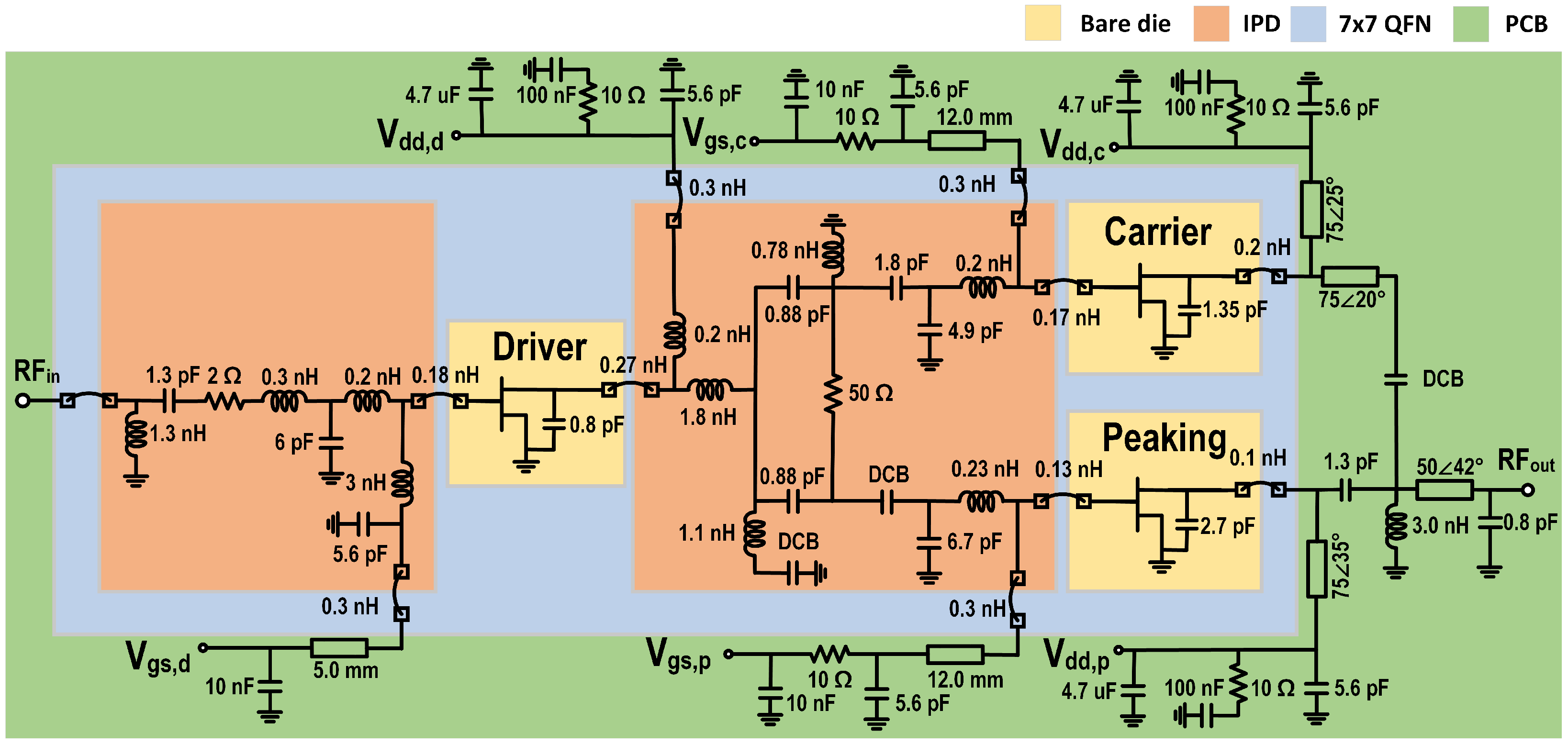
2.1. The Circuits for the 2-Stage DPAM

Figure 1 illustrates the circuit diagram of the proposed 2-stage DPAM implemented using IPD. The proposed DPAM employs a 2-stage single driver structure to achieve high gain and a compact form factor. The main stage incorporates two GaN-HEMT bare dies, serving as the carrier and peaking amplifiers, respectively. The driver stage consists of a single GaN-HEMT bare die. The input and interstage matching networks are compact, achieved through simplification methods and exhibit low loss due to high-Q IPD. These small-sized networks are connected to the GaN-HEMT dies using bond wires for integration into a compact QFN package. The load network is implemented with high-Q surface-mountable passive components on a PCB to ensure high output power with minimal loss. The input matching network for the driver stage, designed using an IPD, features a low-pass structure complemented by an L-section high-pass circuit, transitioning an input impedance from approximately 2 Ω to 50 Ω .

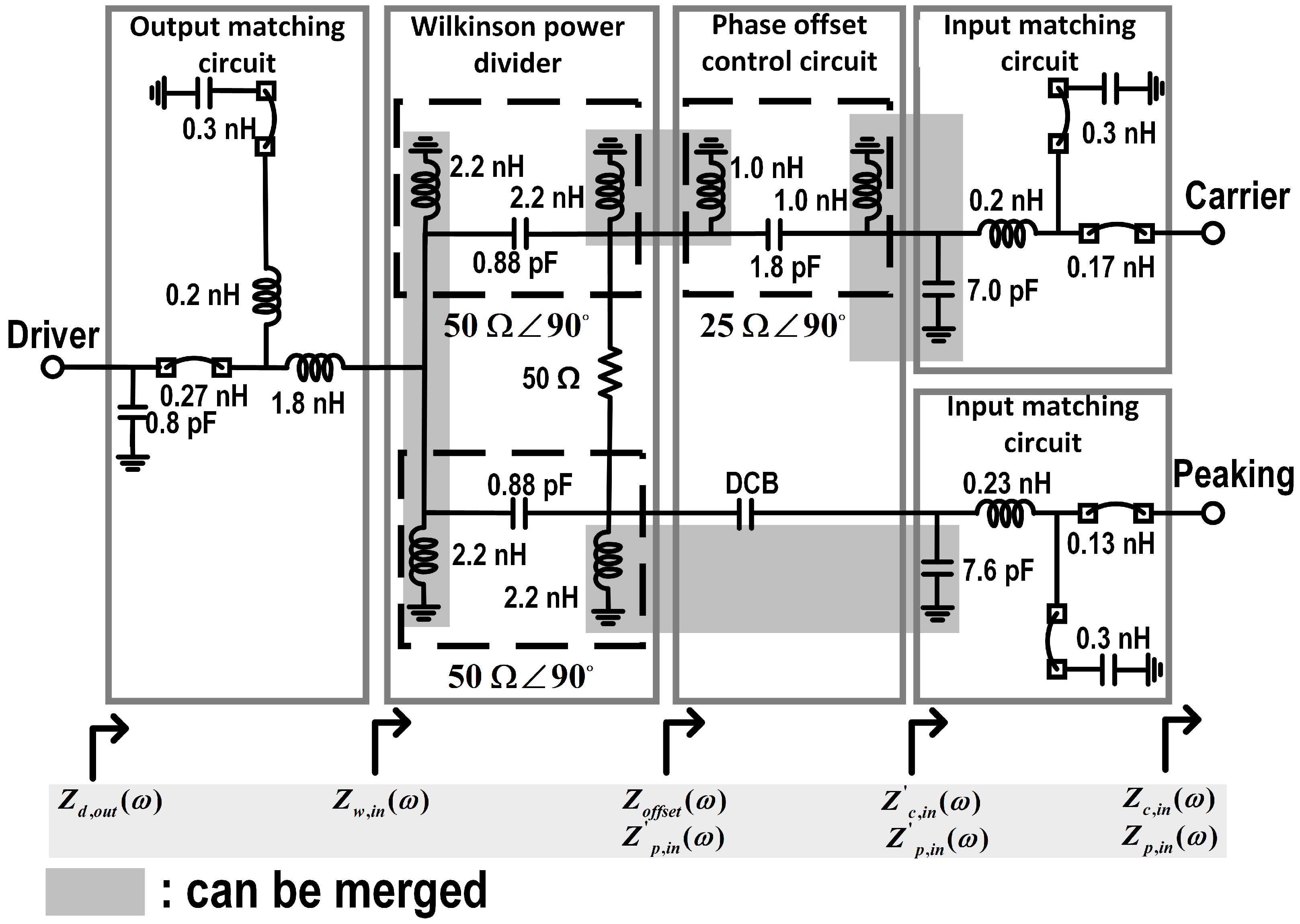
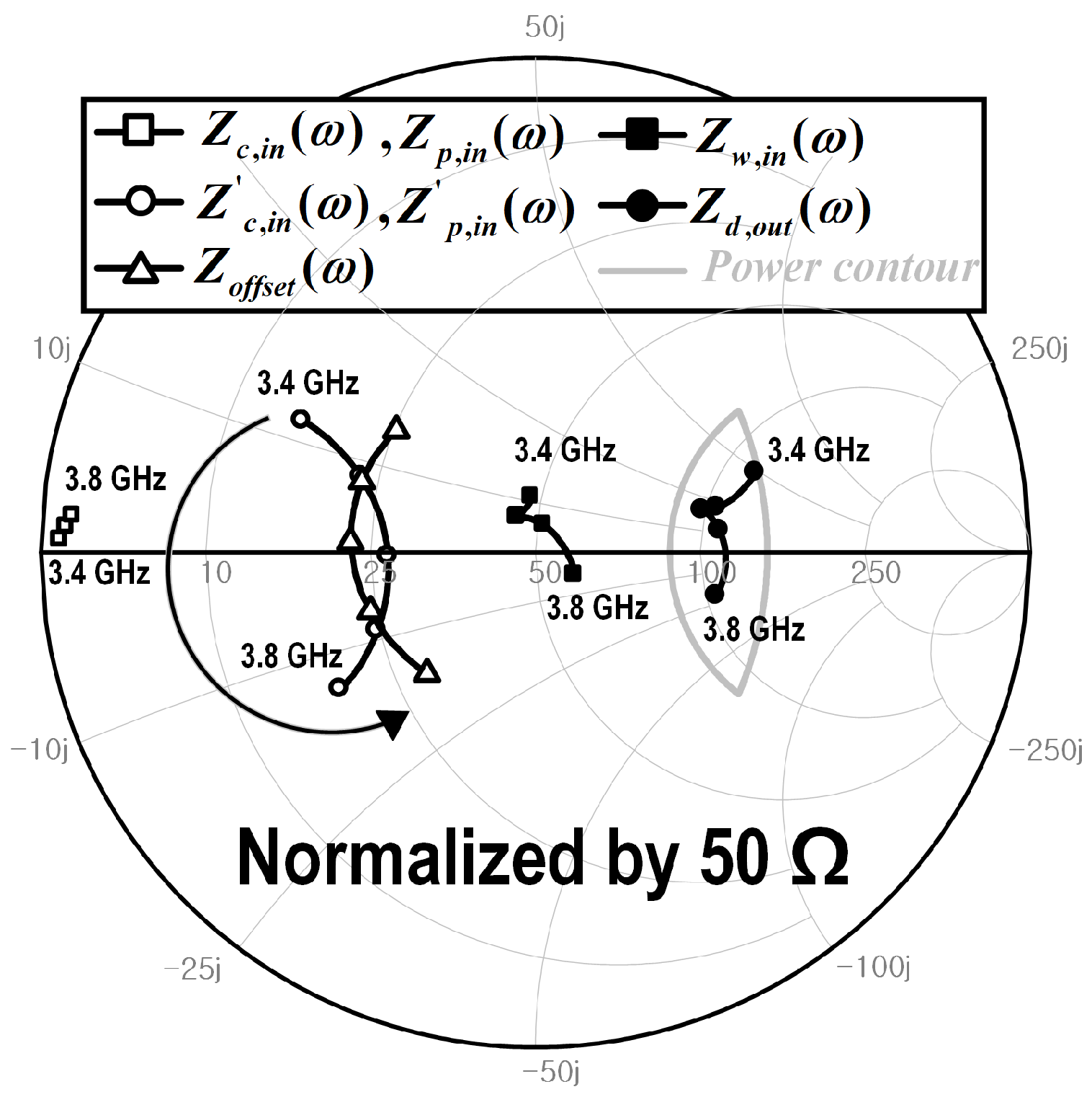
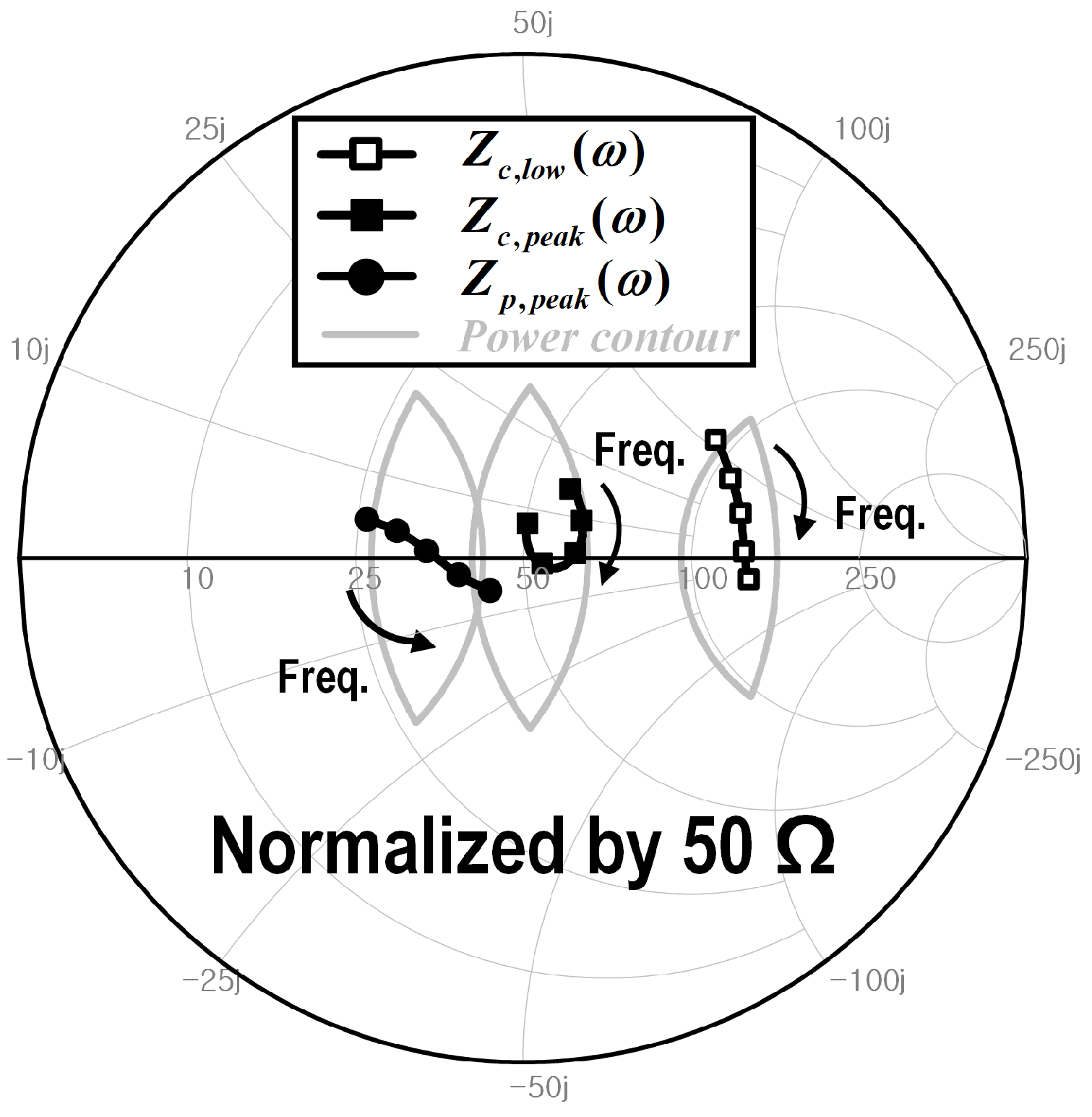
2.2. Interstage Matching Network

Figure 2 depicts a schematic of the interstage matching network utilizing IPD technology to support a single-driver structure. It comprises input matching circuits for the carrier and peaking amplifiers of the main stage, the output matching circuit of the driver stage, a Wilkinson power divider, and the phase offset control circuit. Figure 3 illustrates the impedance transformation within the interstage matching network, featuring a 1 dB power contour for the driver amplifier. The input matching circuits for the carrier and peaking amplifier of the main stage utilize an L-section low-pass structure, inclusive of bond wires, which transforms the input impedances of Z c , i n and Z p , i n , both distributed around 1 Ω , to Z c , i n and Z p , i n for the carrier and peaking amplifiers, respectively. Z c , i n and Z p , i n aim for approximately 25 Ω and feature expansive distribution on the Smith chart. The phase offset control circuit consists of a 25 Ω quarter-wave transmission line (TL), realized through a high-pass L-C-L network, which rotates Z c , i n to Z o f f s e t around the central value of 25 Ω . For power division, the Wilkinson power divider is composed of 50 Ω quarter-wave TLs, designed with lumped elements, to equally split the input power between the carrier and peaking amplifiers of the main stage. The input node impedance of the Wilkinson power divider, Z w , i n , is carefully matched to remain close to 50 Ω . The output matching circuit of the driver amplifier also utilizes an L-section low-pass structure and includes the output capacitance of the transistor and the inductance of bond wires. The output matching network transforms the input node impedance of the Wilkinson power divider, Z w , i n to Z d , o u t for the driver amplifiers, which consistently remains within the 1 dB power contour centered at 100 Ω as demonstrated. Additionally, several shunt components located at the same node have been consolidated into single equivalent components to reduce circuit complexity and improve manufacturability.

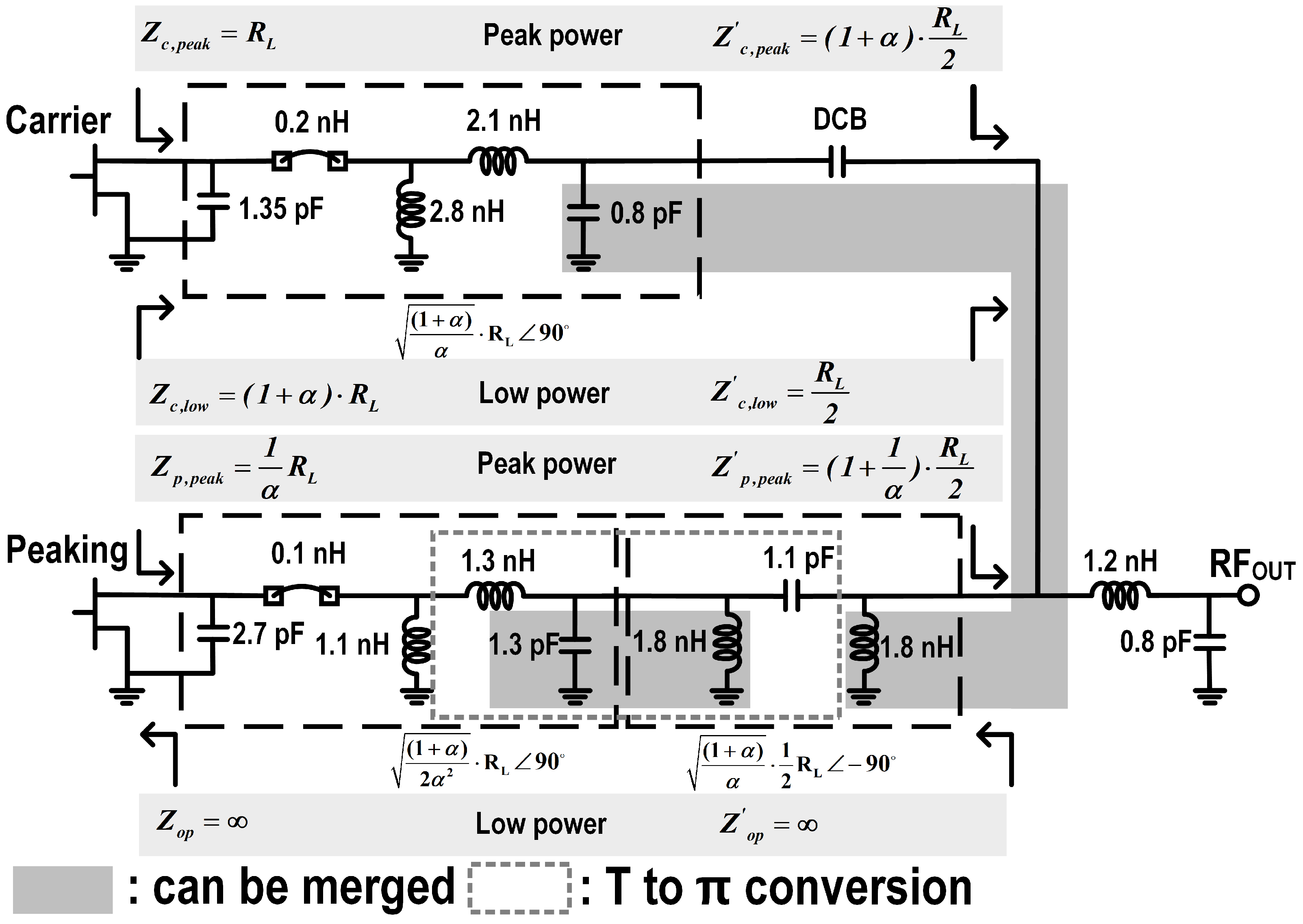
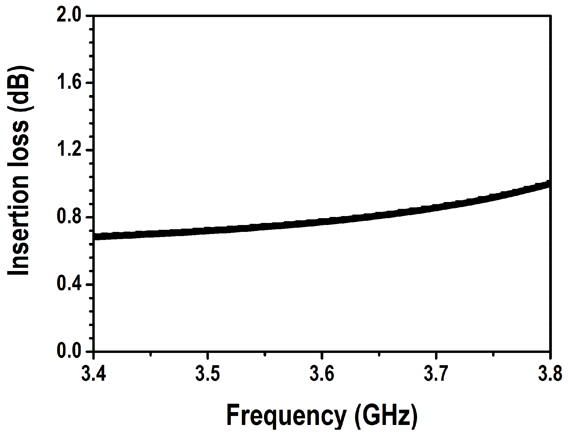
2.3. Load Network Design

Figure 4 shows the schematic of the load network of the proposed 2-stage DPAM, which includes output matching circuits for both the carrier and peaking amplifiers, along with a post matching network. The output matching circuit for the carrier amplifier employs a TL with an electrical length of 90° utilizing the output capacitance of the transistor, bond wires, a shunt inductor for DC supply, an L-section matching circuit, and a DC blocking capacitor. For the peaking amplifier, the output matching circuit consists of a TL with an electrical length of 0°, also including the output capacitance of the transistor, the inductance of the bond wires, a shunt inductor for DC, and an L-section matching network. This structure is further enhanced by a high-pass TL composed of lumped components, offering an equivalent electrical length of −90°. The power combining node and the current source plane’s impedances for both low and peak power levels can be determined using the peak power ratio ( α ) between the carrier and peaking amplifiers. The post matching network consists of a simple L-section low-pass structure that serves to match the output impedance of the combining node to the standard 50 Ω load. In the entire load network, high-Q multi-layer chip capacitors are included, and TLs with high characteristic impedance replace inductors in the matching network.
The proposed DPAM exhibits an output PBO of 8.3 dB, and the peak power ratio α between the carrier and peaking amplifiers is set to 1.6 for asymmetric structures. The optimum load impedance of the carrier amplifier at peak power, marked as R L , is established at 50 Ω . Using these parameter values, other design parameters are derived as illustrated in Figure 4. In addition, to reduce circuit complexity, multiple shunt components located at the same node can be combined into a single equivalent element.
Figure 5 illustrates the distribution of load impedances over frequency at the current source plane for both low and peak power levels. At the low power level, as the peaking amplifier operates in class-C, the output impedance, Z o p , can be approximated as infinity. The class-AB carrier amplifier is matched from Z c , l o w of R L / 2 to Z c , l o w of ( 1 + α ) · R L . For the frequency range of 3.4–3.8 GHz, the load impedances of the carrier amplifier remain within a 1 dB power contour centered at 130 Ω . At peak power level, matching for the carrier amplifier is executed from Z c , p e a k of ( 1 + α ) · ( R L / 2 ) to Z c , p e a k of R L , whereas the peaking amplifier matches from Z p , p e a k of ( 1 + 1 / α ) · ( R L / 2 ) to Z p , p e a k of ( 1 / α ) · R L . In the 3.4–3.8 GHz range, the load impedances of the carrier amplifier stay within a 1 dB power contour centered at 50 Ω , and that of the peaking amplifier also stay within a 1 dB power contour centered at 31 Ω , as demonstrated in Figure 5.
Figure 6 shows the simulated insertion loss of the load network across the frequency range. Achieving high output power and maintaining high efficiency require that insertion loss within the load network be minimized across the operating bandwidth. For this purpose, the load network was designed using high-Q multi-layer chip capacitors and transmission lines (TLs) implemented on a PCB. As a result, the designed load network exhibits an insertion loss ranging from 0.68 to 0.98 dB over the 3.4–3.8 GHz band.

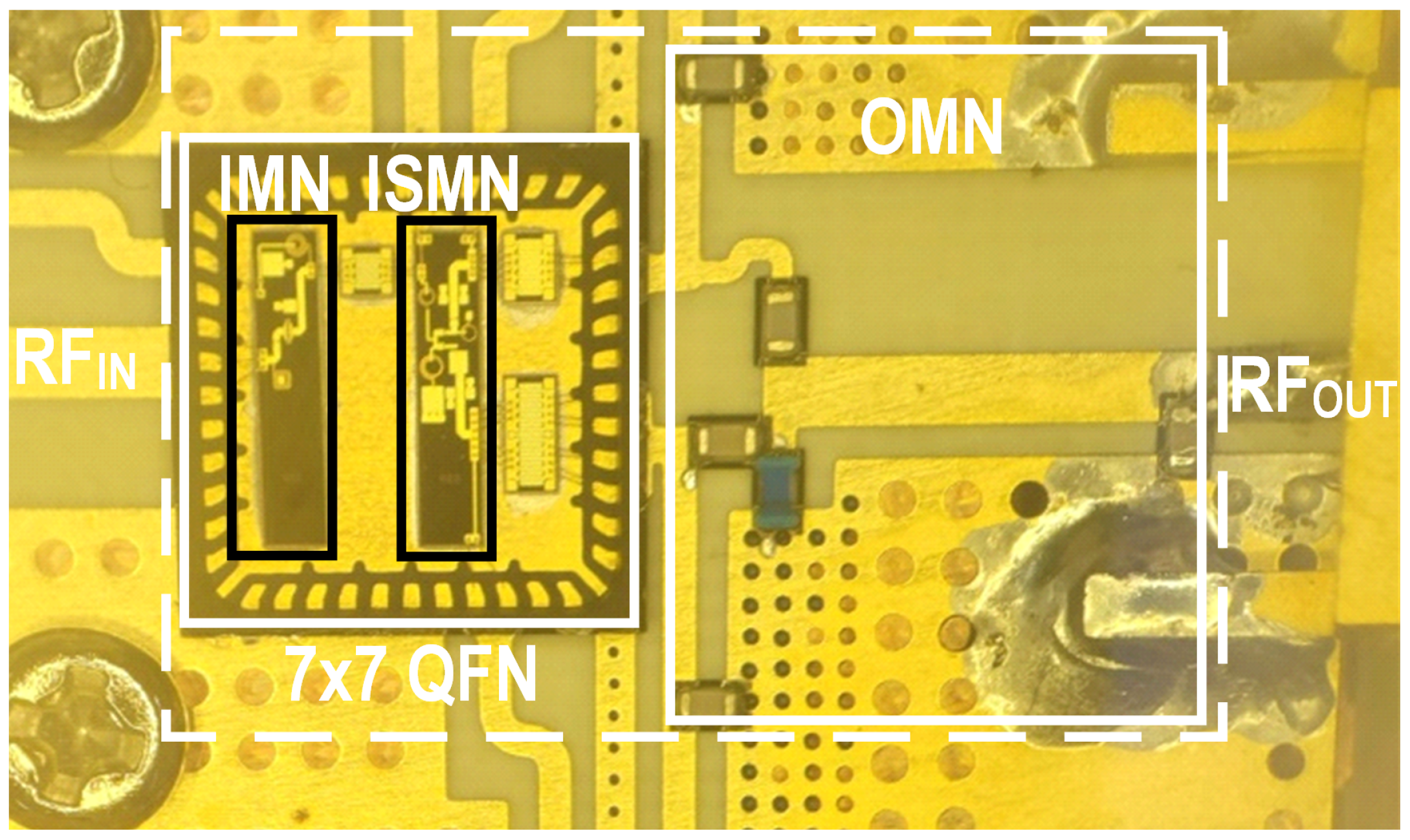
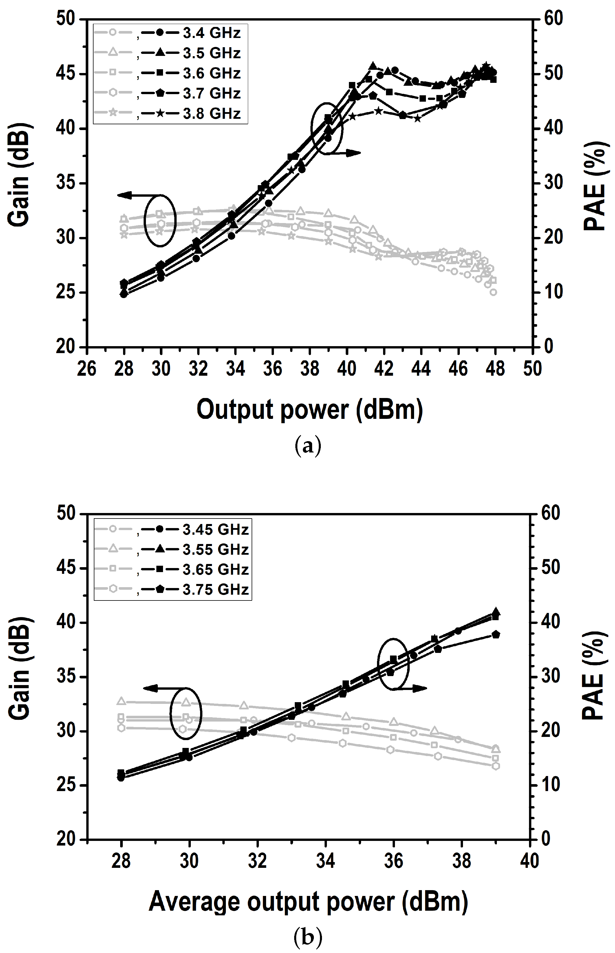
3. Implementation and Measurement

Figure 7 depicts a photograph of the implemented 2-stage DPAM based on IPD on a 7 × 7 QFN. The total area of the DPAM is 9.5 × 14.8 mm2, which includes the external load network. Wavice’s 0.3 μm GaN-HEMT process was used to fabricate the transistor dies for both driver and main stages. The total gate widths of the carrier and peaking amplifiers are 3500 μm and 7000 μm, respectively. The gate width for the driver amplifier is 2100 μm. The interstage and input matching networks were implemented using Wavice’s GaN-on-SiC IPD process, and each IPD block occupies an area of 4700 × 1075 μm2. The evaluation board featuring the load network was designed using Rogers’ 20 mil RO435OB, which exhibits a dielectric constant of 3.48. The load network includes high-Q components consisting of Murata’s GQM series capacitors and LQW series inductors. The drain supply voltage for both the main and driver stages is set at 48 V. Quiescent currents of 30 mA and 50 mA were applied to the driver stage and the carrier amplifier of the main stage, respectively.
Figure 8 displays the measured output power, gain, and PAE:Figure 8a using a pulsed continuous wave (CW) signal with a duty cycle of 10% and a period of 5 ms and Figure 8b using a down-link 5G NR modulated signal with a signal bandwidth of 100 MHz and a PAPR of 9.3 dB. For the 3.4–3.8 GHz band, the DPAM demonstrated peak output power between 47.5 and 47.9 dBm along with efficient performance curves. Using the modulated signal, a power gain between 26.8 and 28.4 dB and a PAE between 37.8 and 41.9% at an average output power of 39 dBm were achieved.
Figure 9a displays the measured ACLR across the carrier frequencies within the 3.4–3.8 GHz, ranging from −19.0 to −28.0 dBc at an average output power of 39.0 dBm. Figure 9b shows the power spectral density (PSD) at a carrier frequency of 3.55 GHz, measured before and after digital predistortion (DPD) was applied. As a result of DPD linearization, the ACLR improved dramatically from −25.21 dBc to −43.01 dBc. Table 1 presents a performance comparison to previously reported results, demonstrating notable efficiency across the frequency band, even with a higher output PBO of 8.5 dB than previous works.

4. Conclusions

This paper presents a GaN 2-stage DPAM on a 7 × 7 QFN package for the 3.4–3.8 GHz band. The input matching network and the interstage matching network were implemented using IPD and integrated with GaN-HEMT bare chips as MCM within the 7 × 7 QFN for the main and driver stages. To minimize insertion loss, the load network was implemented on a PCB, and the low-pass and high-pass structures were initially designed using lumped passive components. These structures were subsequently replaced with TLs featuring high characteristic impedance and high-Q multi-layer chip capacitors to enhance output power and efficiency. Additionally, to reduce circuit complexity, multiple shunt components located at the same node were merged in both the interstage and load matching networks. The DPAM features an output PBO of 8.5 dB using an asymmetric structure. The overall dimensions of the proposed DPAM are 9.5 × 14.8 mm2, including the load network. A gain of over 26.8 dB and a PAE of over 37.8% were achieved at an average output power of 39 dBm in the 3.4–3.8 GHz frequency band in the measurement results when using the downlink 5G NR signal with a bandwidth of 100 MHz and a PAPR of 9.3 dB.

Author Contributions

Conceptualization, S.B. (Sooncheol Bae); methodology, S.B. (Sooncheol Bae) and K.K.; software, S.B. (Soohyun Bin), H.J. and K.B.; validation, S.B. (Sooncheol Bae) and Y.Y.; formal analysis, S.B. (Sooncheol Bae) and Y.C.C.; investigation, S.B. (Sooncheol Bae); resources, Y.W.; data curation, H.K. and W.C.; writing—original draft preparation, S.B. (Sooncheol Bae); writing—review and editing, Y.W. and Y.Y.; visualization, S.B. (Soohyun Bin); supervision, Y.Y.; project administration, Y.Y.; funding acquisition, Y.Y. All authors have read and agreed to the published version of the manuscript.

Funding

This work is supported by Samsung Electronics Co., Ltd. This research was supported by the SungKyunKwan University and the BK21 FOUR (Graduate School Innovation) funded by the Ministry of Education (MOE, Republic of Korea) and National Research Foundation of Korea (NRF).

Data Availability Statement

Data is contained within the article.

Conflicts of Interest

The Authors Kuhyeon Kwon, Hyunuk Kang, Woojin Choi, and Youngyun Woo were employed by the company Samsung Electronics Co., Ltd. Authors Hyeongjin Jeon, Kyungdong Bae, and Youngoo Yang were employed by the company para-PA Inc. The remaining authors declare that the research was conducted in the absence of any commercial or financial relationships that could be construed as a potential conflict of interest.

References

  1. Kim, B.; Kim, J.; Cha, J. The Doherty power amplifier. IEEE Microw. Mag. 2006, 7, 42–50. [Google Scholar] [CrossRef]
  2. Oh, H.; Kang, H.; Lee, H.; Koo, H.; Kim, M.; Lee, W.; Lim, W.; Park, C.-S.; Hwang, K.C.; Lee, Y.-K.; et al. Doherty power amplifier based on the fundamental current ratio for asymmetric cells. IEEE Trans. Microw. Theory Tech. 2017, 65, 4190–4197. [Google Scholar] [CrossRef]
  3. Choi, Y.C.; Choi, W.; Oh, H.; Chen, Y.; Shin, J.; Jeon, H.; Hwang, K.C.; Lee, K.-Y.; Yang, Y. Doherty power amplifier with extended highefficiency range based on the utilization of multiple output power back-off parameters. IEEE Trans. Microw. Theory Tech. 2022, 70, 2258–2270. [Google Scholar] [CrossRef]
  4. Chen, Y.; Choi, W.; Shin, J.; Jeon, H.; Bae, S.; Choi, Y.C.; Woo, S.; Woo, Y.Y.; Oh, H.; Lee, K.-Y.; et al. Generalized expression and design method of modified load networks for Doherty power amplifier with extended back-off range. IEEE Access 2022, 10, 77487–77497. [Google Scholar] [CrossRef]
  5. Choi, W.; Shin, J.; Chen, Y.; Jeon, H.; Choi, Y.C.; Bae, S.; Woo, Y.Y.; Kang, H.; Yang, Y. Two-Stage Doherty Power Amplifier Using Broadband Interstage Matching Network. IEEE Microw. Wirel. Technol. Lett. 2023, 33, 1454–1457. [Google Scholar] [CrossRef]
  6. Lee, H.; Kwon, J.; Lim, W.; Lee, W.; Kang, H.; Hwang, K.C.; Lee, K.-Y.; Park, C.-s.; Yang, Y. Optimized current of the peaking amplifier for two-stage Doherty power amplifier. IEEE Trans. Microw. Theory Tech. 2017, 65, 209–217. [Google Scholar] [CrossRef]
  7. Ghim, J.; Cho, K.; Kim, J.; Stapleton, S.P. A high gain Doherty amplifier using embedded drivers. In Proceedings of the 2006 IEEE MTT-S International Microwave Symposium Digest, San Fransisco, CA, USA, 11–16 June 2006; pp. 1838–1841. [Google Scholar]
  8. Abounemra, A.M.E.; Chen, W.; Huang, F.; Maktoomi, M.; Zhang, W.; Helaoui, M.; Ghannouchi, F.M. Systematic design methodology of broadband Doherty amplifier using unified matching/combining networks with an application to GaN MMIC design. IEEE Access 2017, 9, 5791–5805. [Google Scholar] [CrossRef]
  9. Lee, H.; Lim, W.; Bae, J.; Lee, W.; Kang, H.; Hwang, K.C.; Lee, K.-Y.; Park, C.-S.; Yang, Y. Highly efficient fully integrated GaN-HEMT Doherty power amplifier based on compact load network. IEEE Trans. Microw. Theory Tech. 2017, 65, 5203–5211. [Google Scholar] [CrossRef]
  10. Lin, H.C.; Chang, D.C.; Fan, T.H.; Chiou, H.K. A 3.6–4.5 GHz Doherty RF Power Amplifier Using 0.25 um GaN/SiC HEMT and GaAs IPD Technology. In Proceedings of the 2023 IEEE CPMT Symposium Japan (ICSJ), Kyoto, Japan, 15–17 November 2023; pp. 156–159. [Google Scholar]
  11. Chang, D.P.; Noh, Y.S.; Yom, I.B. GaN high power amplifier MMIC for 30 W compact Doherty amplifier for LTE active antenna system. In Proceedings of the 2015 10th European Microwave Integrated Circuits Conference (EuMIC), Paris, France, 7–8 September 2015; pp. 265–268. [Google Scholar]
  12. Dai, W.; Luo, S.; Wu, Q.; Xu, R.; Yan, B.; Wu, C.; Xu, Y. A 2.6-GHz-band High power GaN Doherty Power Amplifier Based on GaAs Integrated Passive Devices. In Proceedings of the 2023 IEEE MTT-S international Microwave Workshop Series on Advanced Materials and Processes for RF and THz Applications (IMWS-AMP), Chengdu, China, 13–15 November 2023; pp. 1–3. [Google Scholar]
Figure 1. Schematic of the proposed 2-stage DPAM.
Electronics 14 02398 g001
Figure 2. Schematic of the interstage matching network using an IPD.
Electronics 14 02398 g002
Figure 3. Impedance transformation with a 1 dB output power contour for the driver amplifier.
Electronics 14 02398 g003
Figure 4. Schematic of the load network.
Electronics 14 02398 g004
Figure 5. Distribution of load impedance over frequency at the current source plane for low power and peak power levels.
Electronics 14 02398 g005
Figure 6. Insertion loss of load network over frequency.
Electronics 14 02398 g006
Figure 7. Implemented 2-stage DPAM on a 7 × 7 QFN.
Electronics 14 02398 g007
Figure 8. Measured output power, gain, and PAE: (a) pulsed CW, (b) 5G NR signal.
Electronics 14 02398 g008
Figure 9. Measured ACLR (a), and PSD before and after DPD at the carrier frequency of 3.55 GHz (b).
Electronics 14 02398 g009
Table 1. Performance comparison to the previously reported 2-stage DPAs.
Ref.TypeProcessDriverFreq.PavgOutput PBOGainavgPAEavgACLR SignalSize
(IPD)Topology(GHz)(dBm)(dB)(dB)(%)(dBc) (mm2)
[6]Hybrid ModuleGaN-HEMTDual2.65547.86.025.053.0 *−30.0/
LTE136 × 120
[8]MMICGaN-HEMTDual3.3–3.736.06.027.4–30.638.0–52.0−25.5/
−47.0
LTE4.4 × 3.5
[10]MCMGaN-HEMT (GaAs)Dual3.6–4.529.96.018.532.8N/A5G NR8.18
This workMCMGaN-HEMT (GaN)Single3.4–3.839.08.526.8–28.437.8–41.9−25.0/
−47.0
5G NR7.0 × 7.0
* Drain efficiency, Before linearization/after linearization, N/A: Not Available.
Disclaimer/Publisher’s Note: The statements, opinions and data contained in all publications are solely those of the individual author(s) and contributor(s) and not of MDPI and/or the editor(s). MDPI and/or the editor(s) disclaim responsibility for any injury to people or property resulting from any ideas, methods, instructions or products referred to in the content.

