Next Article in Journal
Design of a Land Area Measuring Instrument Based on an STM32 and a BeiDou Positioning Chip
Previous Article in Journal
GNSS Spoofing Detection Based on Wavelets and Machine Learning
Previous Article in Special Issue
Theoretical Design and Simulation of a Dual-Band Sheet Beam Extended Interaction Oscillator
 
 
Due to scheduled maintenance work on our database systems, there may be short service disruptions on this website between 10:00 and 11:00 CEST on June 14th.
Article

Co-Design of Single-Layer RCS-Reducing Surface and Antenna Array Based on AMC Technique

1
The School of Electronic and Information Engineering, Nanjing University of Information Science and Technology, Nanjing 210044, China
2
Institute of Electronic Engineering, China Academy of Engineering Physics, Mianyang 621900, China
*
Authors to whom correspondence should be addressed.
Electronics 2025, 14(12), 2392; https://doi.org/10.3390/electronics14122392
Submission received: 8 May 2025 / Revised: 1 June 2025 / Accepted: 10 June 2025 / Published: 11 June 2025
(This article belongs to the Special Issue Broadband High-Power Millimeter-Wave and Terahertz Devices)

Abstract

:
A co-design of radar cross section (RCS) reducing surface and array antenna on a single-layer printed board is presented in this paper. To achieve this goal, two kinds of artificial magnetic conductors (AMCs) are designed and optimized. The first kind of AMC shares the same geometry with the array element and thus is simultaneously used as the array element. The other kind of AMC generates opposed-phased reflections for a normal incident wave, and when they are in a checkerboard configuration, the RCS is reduced via phase cancellation of opposed-phased reflections. In the range of 10 GHz to 16 GHz, the designed bi-functional surface achieves an 8 dB decline in monostatic RCS, while the array antenna obtains a gain of 15 dBi, a side-lobe less than −10 dB, and a cross-polarization less than −20 dB at 13.5 GHz. To validate the calculation results, a prototype is fabricated and measured. To feed the array antenna, a T-type power divider network is etched under the ground and the array is fed via coupling slots on the ground. The measured results agree with the simulation results.

1. Introduction

Radar cross section (RCS) reduction has garnered great attention in the development of stealth platforms such as unmanned aerial vehicles, cruise missiles, and war ships [1]. On the other hand, these stealth platforms also need wireless communication systems to navigate, detect, and send or receive commands. In order to increase the gain of the antenna, the common solution is to enlarge the antenna’s radiation aperture. However, the large radiation aperture will significantly increase the RCS and worsen the stealth of the platforms. There are usually some trade-offs between the antennas and RCS reduction because the two functions of directional radiation enhancement and radiation attenuation are generally contradictory.
The common method is to apply various coatings or radar-absorbent materials to the antennas’ surface. For the out-of-band frequency, the wave backscattered towards the opponent radar will be efficiently reduced and the antenna performance will be preserved [2,3,4,5]. However, this method is still incompetent in relation to the in-band co-design of RCS reduction and antenna. For example, researchers in [3] covered the patch antenna with an absorbent frequency selective radome (AFSR). The AFSR is designed with a transmission window at 8.90 GHz and two separate absorption bands (from 4.8 to 7.5 GHz and from 10 to 13 GHz) while the patch antenna works at 8.9 GHz. Another disadvantage of this approach is that the introduced coating leads to the increase in thickness as well as weight. The co-design of RCS reduction and antenna array on a single layer is therefore more attractive. Recently, new two-dimensional materials such as artificial magnetic conductors (AMCs) [6,7] and polarization conversion metasurfaces (PCMs) [8] have been widely used in RCS reduction. Generally, the working mechanism of RCS reduction based on AMCs is that two different AMC unit cells in a checkerboard arrangement provide out-of-phase reflections, thus reducing the scattering towards the backscatter direction via phase cancellation. The checkerboard-arranged PCM works via a similar mechanism in which two PCM unit cells convert the incident wave to its opposite cross-polarizations, which then cancel each other out. By removing some AMC or PCM units and replacing them with the array antenna or arranging the antenna array with AMC or PCM units, the co-design of the RCS-reducing surface and antenna array on a single layer is realized [9,10,11]. For example, a microstrip antenna operating at 10.5 GHz is proposed in [9], and an in-band RCS from 8.8 GHZ to 17.3 GHz is realized by two AMC unit cells in a checkerboard configuration around the microstrip antenna.
Another method is by shaping the array units to the AMC or PCM; in other words, designing the bi-functional units to simultaneously generate radiation and reduce the backward RCS [12,13,14,15,16,17,18,19,20,21]. For example, P. Wang et al. proposed a circularly polarized antenna array with a low RCS based on PCM [13] without increasing the structural complexity. The PCM patch is cut into two separated units. The radiation is realized by feeding the small units, and the polarization conversion relies on the slots between the two separated units. The bi-functional unit of radiation and PCM scattering has great advantages in the co-design of RCS reduction and antenna array. Similarly, the bi-functional units with radiation and AMC scattering also have the potential to be used as a co-design strategy. D. Zhang et al. proposed an orbital angular momentum (OAM) antenna with RCS reduction based on bi-function strategy [16]. Two kinds of AMC units are designed with opposed-phased reflections and similar radiation patterns. This strategy can be implemented into the co-design of far-field antennas and RCS reduction surfaces. However, this strategy will also lead to a narrow-band RCS reduction. To realize similar radiation patterns and opposed-phased reflections, resonance is introduced by slots, which leads to a narrow bandwidth of opposed-phased reflections. Y. Liu et al. used two different antenna elements, which have similar radiation performances and different reflection phases, to form a low RCS patch antenna array [18]. The X-polarization scattering between two elements is out of phase and will cancel each other, and the Y-polarization incident wave will be absorbed by the antenna elements. Generally, studies on the integration of scattering reduction and radiation using PCM technology demonstrate superior performance, whereas research based on the AMC technology remains in a less mature stage.
This paper proposes a co-design of RCS reduction and array antenna based on a single-layer AMC surface. The proposed co-design is based on a bi-functional strategy, and we make improvements to guarantee a broad RCS reduction without increasing the structural complexity. This work is organized as follows. Section 2 discusses the design strategy and the configuration of the patch units, and gives the radiation performances and scattering performance of the proposed bi-functional surface. Section 3 conducts the fabrication and far-field measurement. Finally, Section 4 concludes the article.

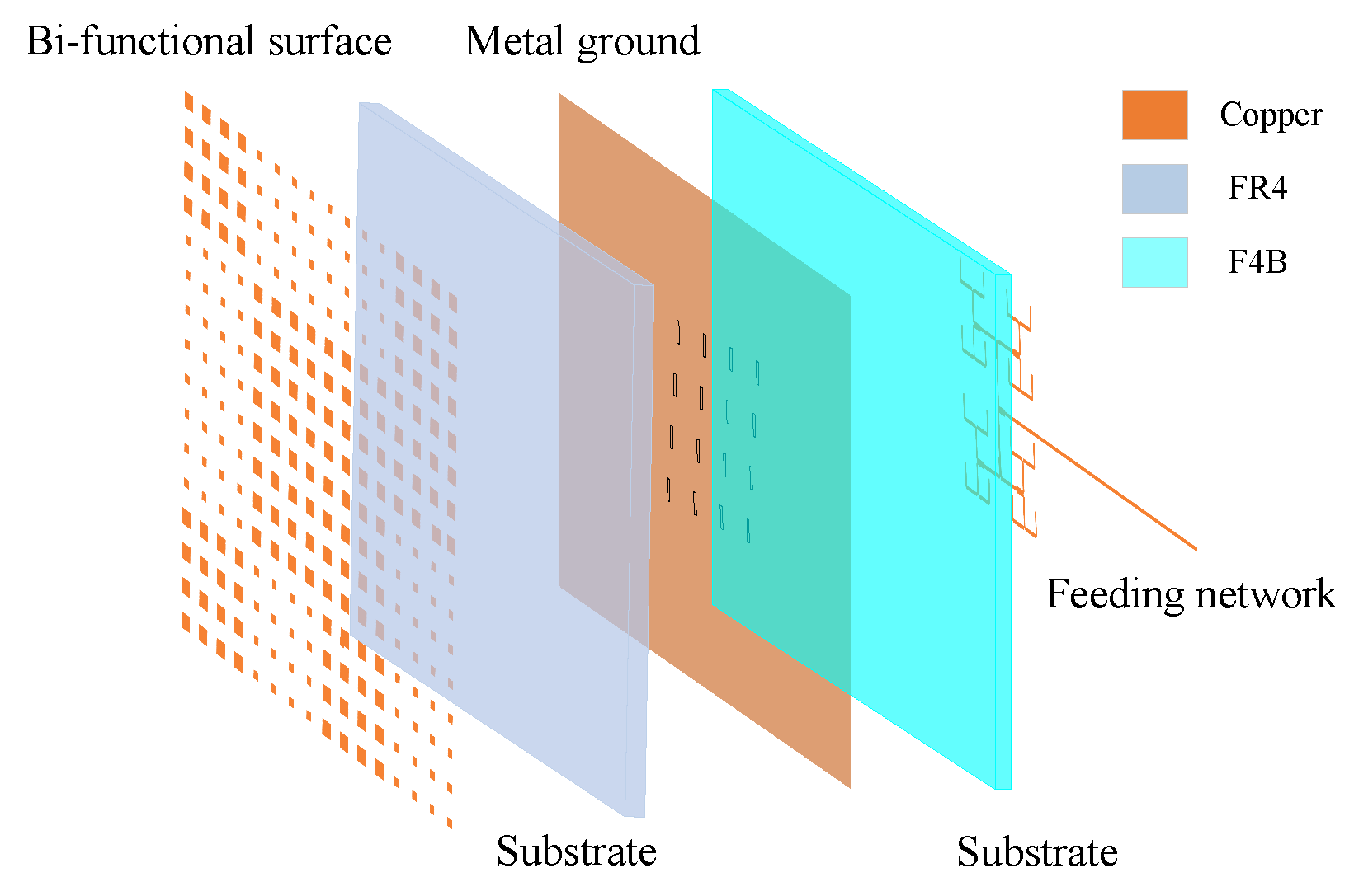
2. Co-Design Strategy and Implementation

2.1. Co-Design Strategy

The RCS reduction of the AMC surface is based on phase cancellation, which requires two kinds of AMC surfaces to provide opposed-phased reflections. Simultaneously, the antenna units an have in-band radiation pattern. Furthermore, we do not introduce additional structures that may complicate the device. Considering the three requirements, one feasible co-design strategy is to assign one kind of AMC with a bi-function of reflection and radiation and assign the other kind of AMC with opposed-phased reflection to reduce the RCS. The co-design procedure is as follows:
(1)
Configure the patch shape according to the requirements of the antenna, including the operating frequency, the gain, the side-lobe level, and the polarization. This patch is named as the radiation-scattering AMC unit.
(2)
Design the second AMC unit, which has the opposed-phased reflection unlike the radiation-scattering AMC unit. This unit is named as the opposed-phase AMC unit.
(3)
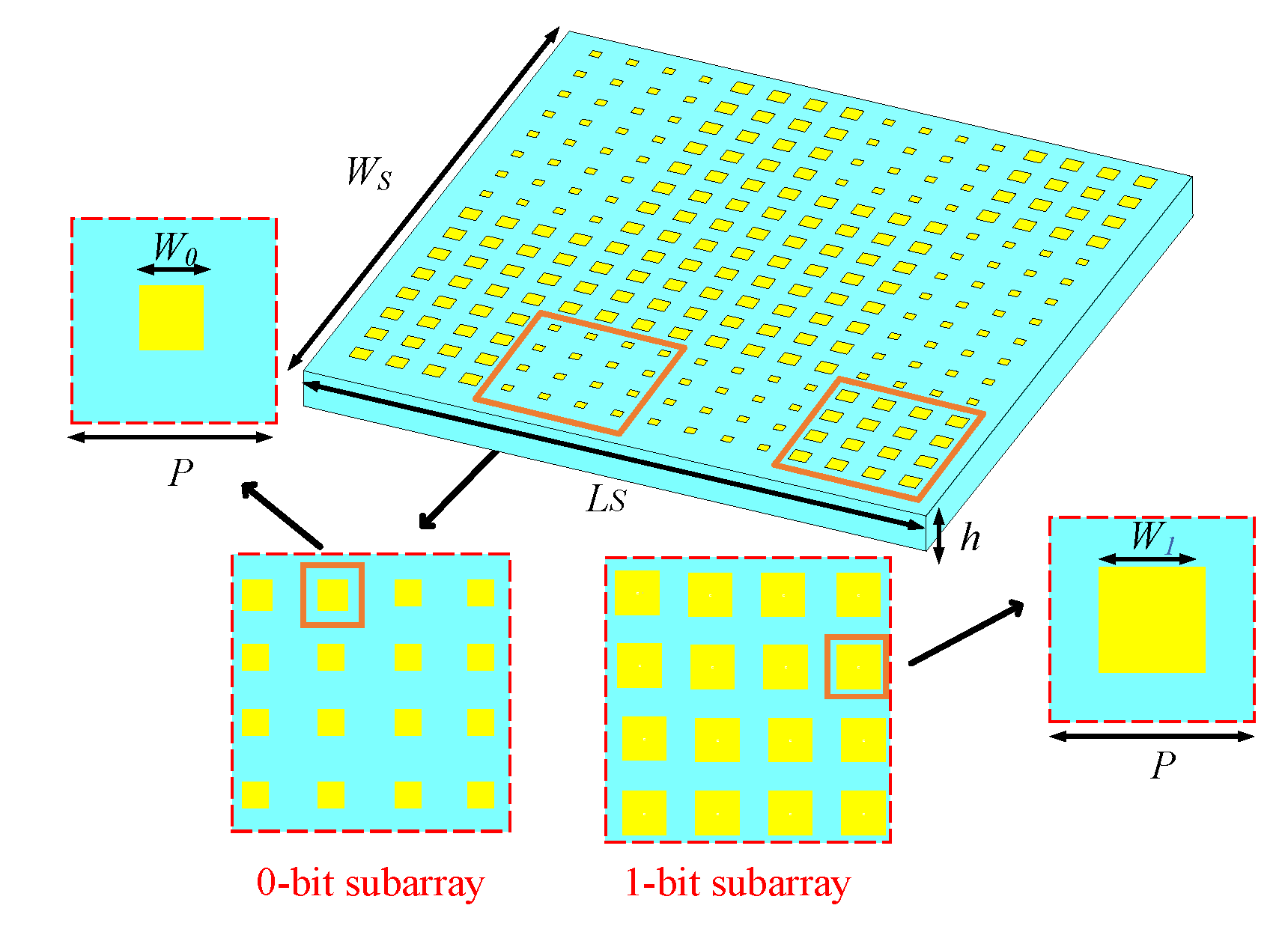
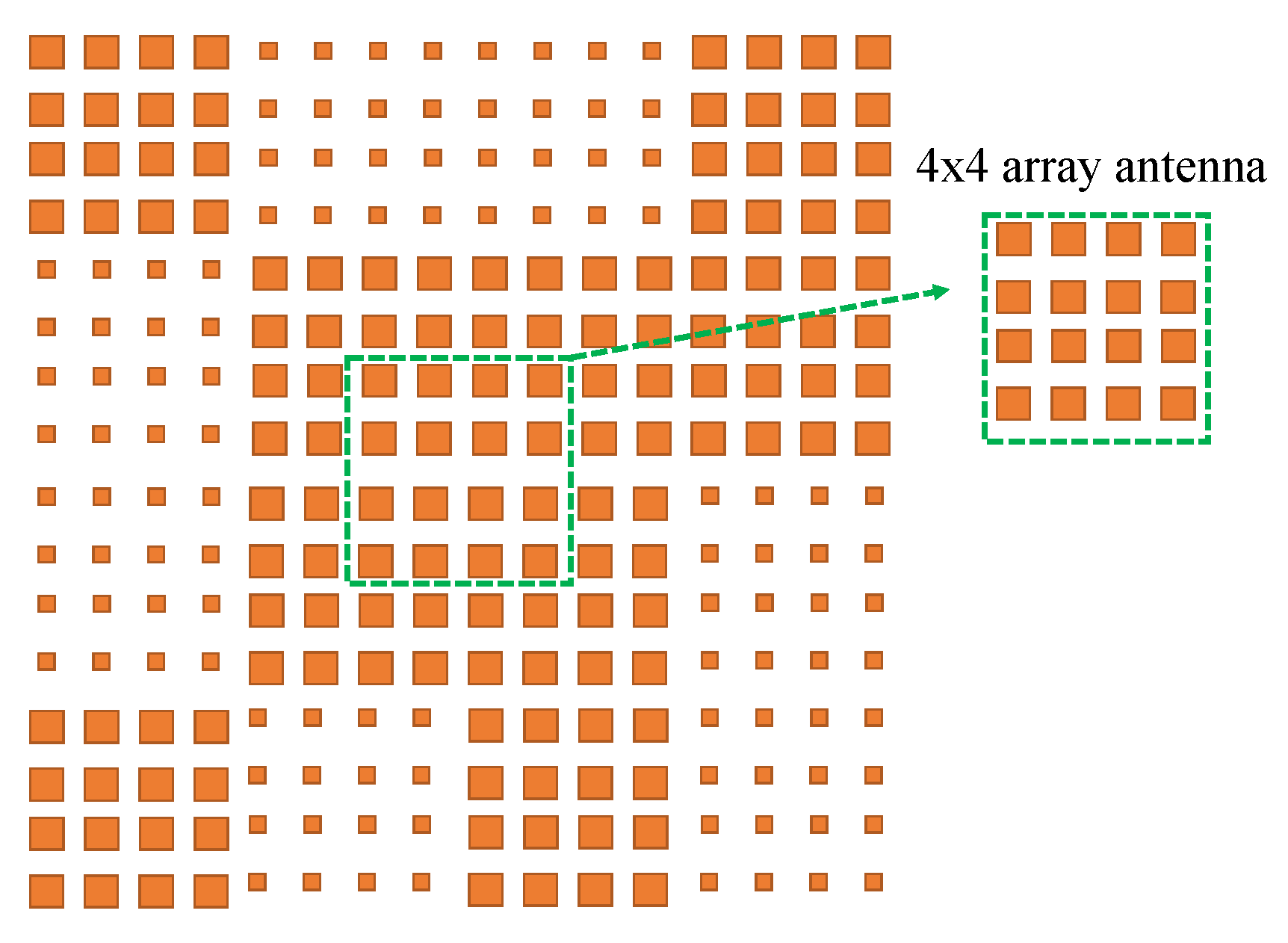
Configure the checkerboard configuration of the two AMC units and choose the suitable radiation-scattering AMC units to form the antenna array.
(4)
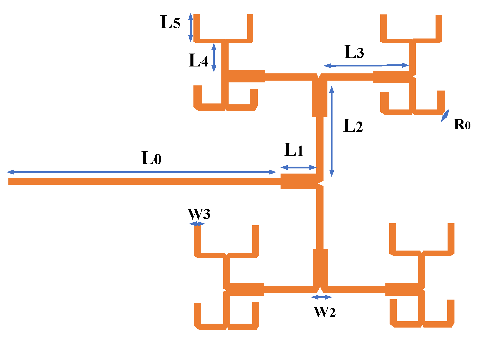
Design the feeding network according to the antenna array layout.
In summary, we assigned the bi-functions of reflection and radiation to one kind of AMC unit and designed the other kind of AMC unit for the opposed-phase matching. Such an arrangement ensures opposed-phased reflection between the two kinds of AMC units in a broad bandwidth and further ensures broadband RCS reduction.

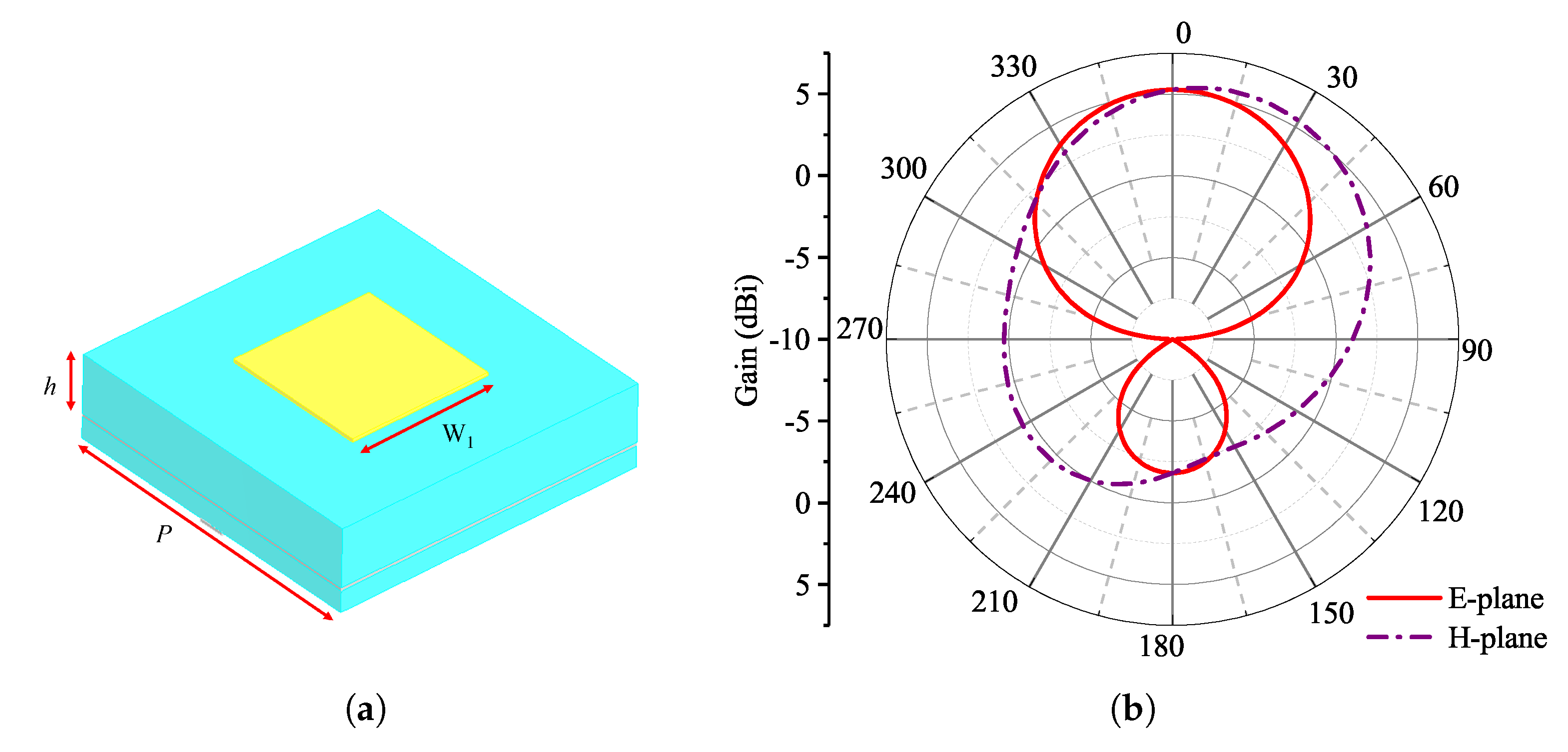
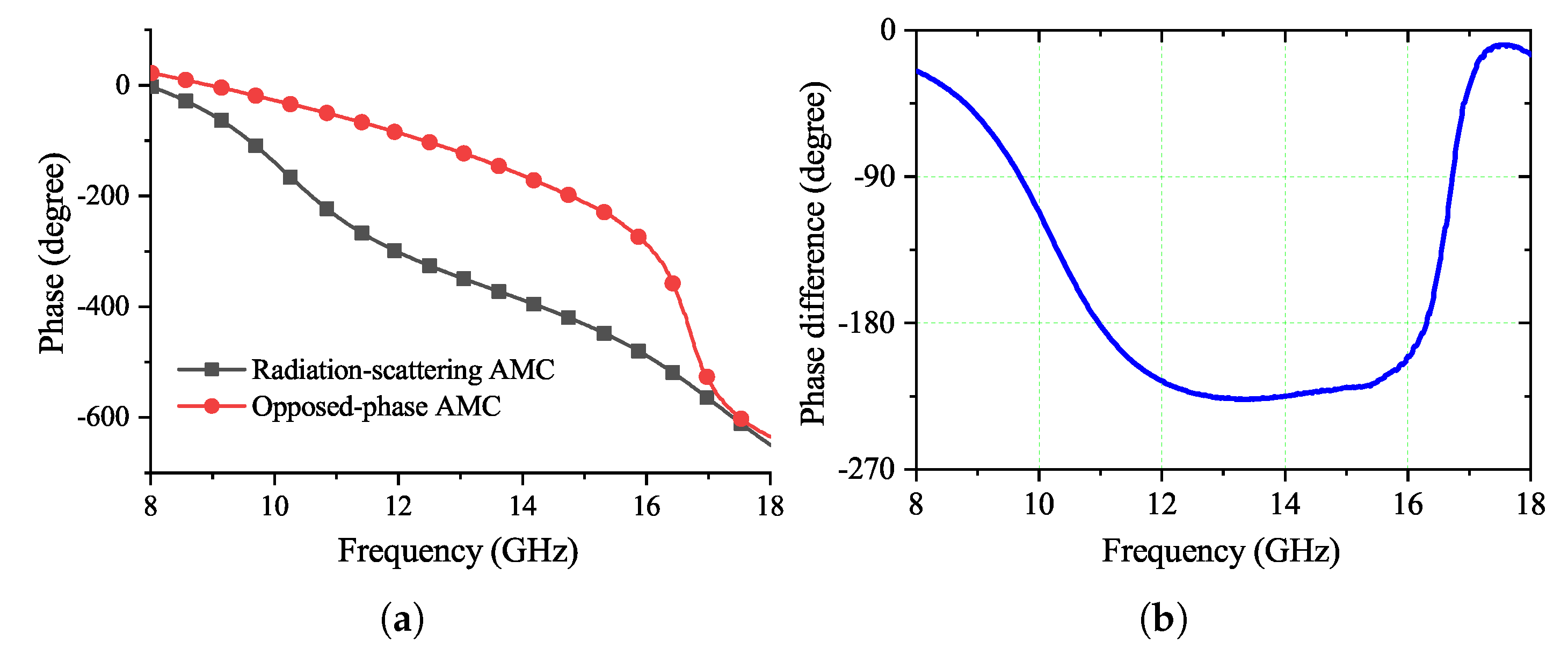
2.2. Radiation-Scattering AMC and Opposed-Phase AMC
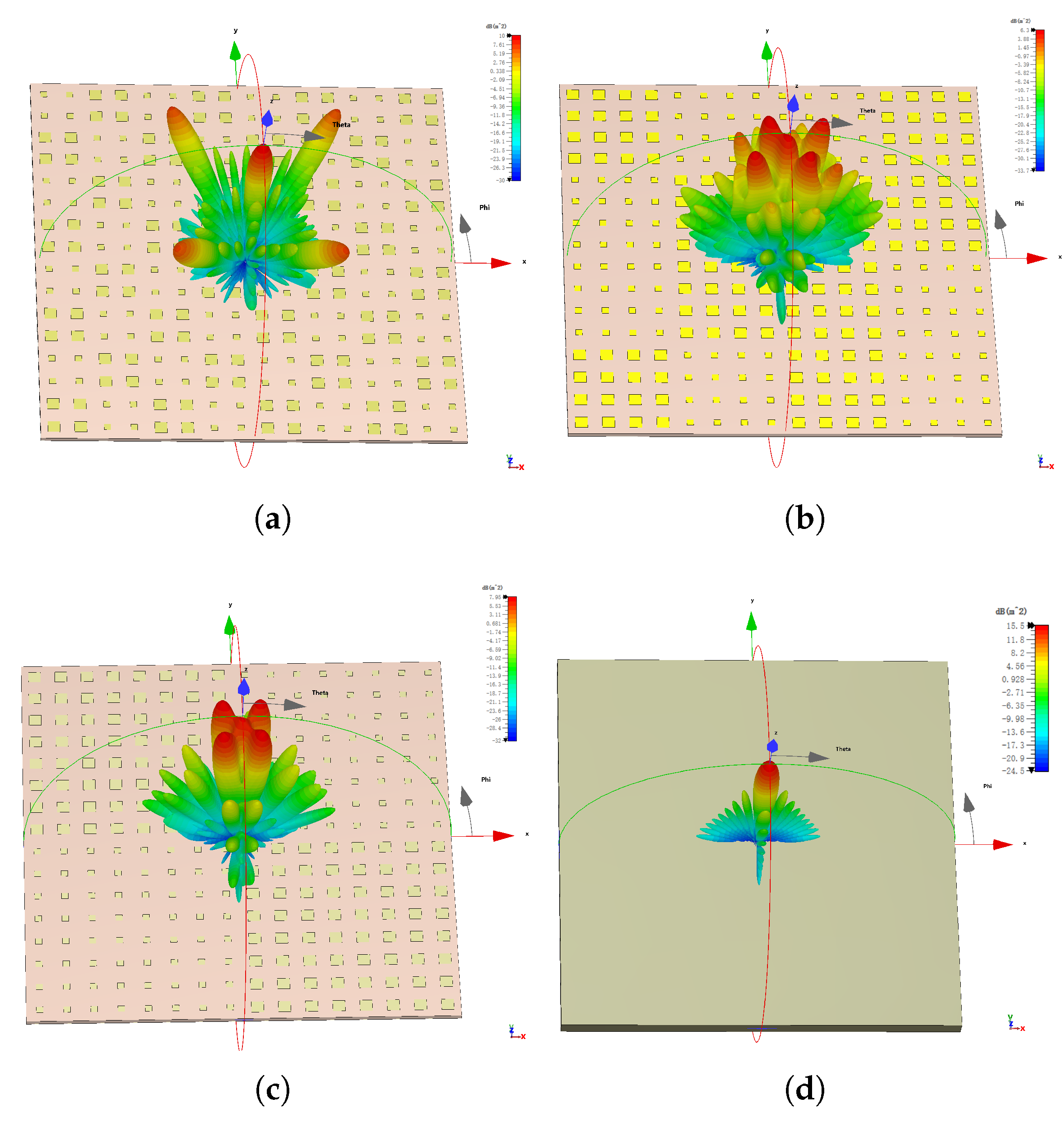
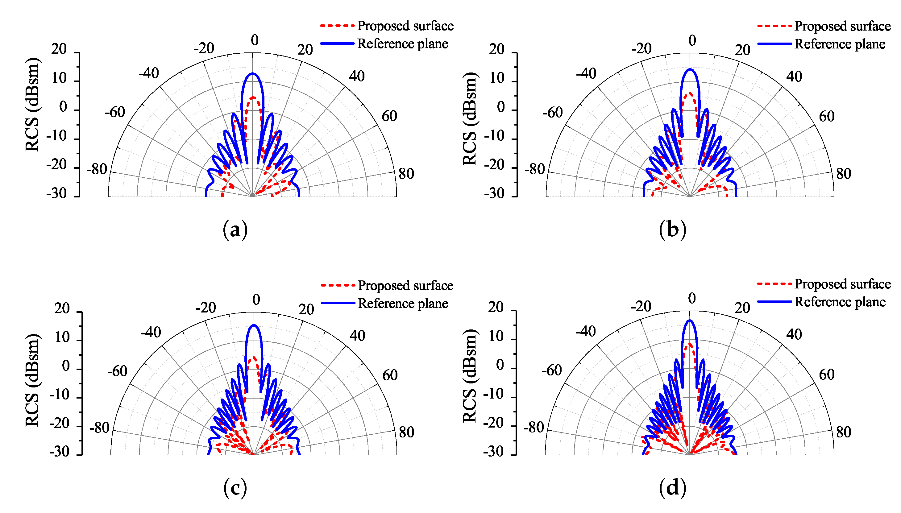
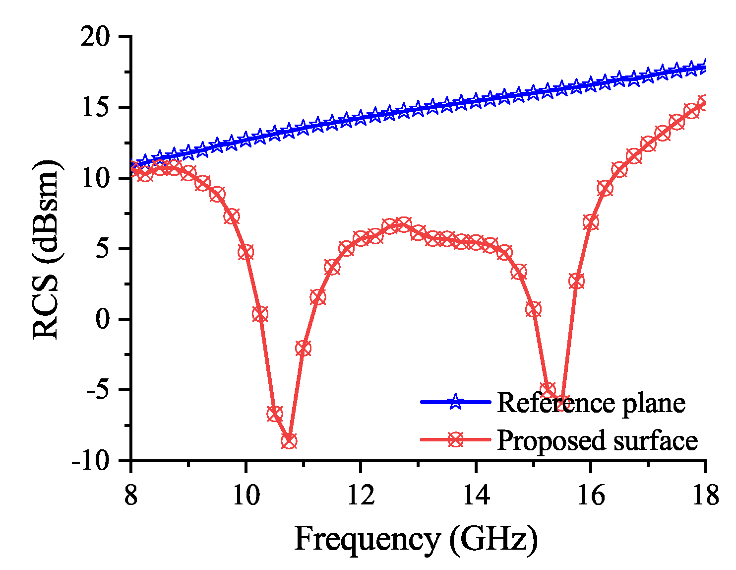
Following the above procedures, a single-layer surface with bi-functions of RCS reduction and array antenna is designed. The operating frequency f 0 of the antenna is set as 13.5 GHz, and the substrate material is FR4 with a relative permittivity ϵ r of 4.3, a loss tangent of 0.025, and a height h of 2.2 mm. According to the experience formula of patch antenna [22],
W = c 2 f 0 2 ε r + 1
ε e f f = ε r + 1 2 + ε r 1 2 1 + 12 h W
L = c 2 f 0 ε e f f 0.842 h ε e f f + 0.3 W h + 0.264 ε e f f 0.258 W h + 0.8
the width of the patch W is 6.82 mm and the length of the patch L is 4.18 mm. Since stealth platforms prefer RCS reduction along any polarizations, the radiation-scattering AMC unit should have geometric symmetry. Therefore, the patch is set to a square and the width W 1 is set as the average value of W and L, in other words, W 1 is 5.5 mm.
W 1 = W + L / 2
Figure 1 gives the radiation pattern of the radiation-scattering AMC unit. The radiation pattern along the E-plane exhibits a highly symmetric distribution, while the radiation pattern along the H-plane is relatively symmetric. According to the common arrangement scheme of array antenna, the periodic length P of the radiation-scattering AMC unit is about half of the wavelength. Moreover, the radiation-scattering AMC unit and the opposed-phase AMC unit should have the same periodic length. Considering the two requirements, P is set as 12 mm.
Now that the geometry of the radiation-scattering AMC unit is fixed, we move on to designing the opposed-phase AMC unit. After conducting parameter sweeping, the patch width W 0 of the opposed-phase AMC unit is set as 3 mm. The reflection phase of the radiation-scattering AMC and opposed-phase AMC units is given in Figure 2 under a periodic boundary. As it can be seen, from 10.2 GHz to 16.4 GHz, the reflection phases of the two AMC units have a difference close to 180 ± 47 . According to the analysis in [23], a phase difference of 180 ± 37 ensures an RCS reduction that is larger than 10 dB. This indicates that the proposed two kinds of AMCs have the potential to realize an RCS reduction close to 10 dB.

2.3. RCS Reduction

The next procedure is configuring the checkerboard configuration of the two AMC units. The ideal AMC units are placed under periodic infinite boundary. In practice, two kinds of AMC units are first placed by N rows and N columns to form N × N sub-arrays, and then the two sub-arrays are arranged alternately in a finite surface. We choose 16 radiation-scattering AMC units placed in 4 rows and 4 columns to form the 1-bit sub-array, and 16 opposed-phase AMC units placed in 4 rows and 4 columns to form the 0-bit sub-array. Periodic boundary is approximately implemented within each sub-array. The checkerboard configuration of the two sub-arrays is given in Figure 3. To facilitate the arrangement of the antenna array, four 1-bit sub-arrays are placed at the center of surface. Figure 4 shows the 3D reflection pattern of the surface with the 2 × 2 sub-array, 4 × 4 sub-array, and 8 × 8 sub-array under a normal injection. For comparison, a metal surface with the same shape is used as the reference plane. As can be seen, the reflection pattern of the metal surface exhibits a single beam in the normal direction, while the reflection pattern of the proposed surface has multiple beams. Owing to the phase cancellation of AMC units, the injection beam is refracted into an oblique direction and the normal reflection is attenuated compared with the reference plane. The surfaces with 2 × 2, 4 × 4, and 8 × 8 sub-array arrangements, respectively, show a maximum RCS of 10 dBsm, 6.3 dBsm, and 7.95 dBsm. This proves that the 4 × 4 sub-array arrangement leads to a better RCS reduction. Figure 5 shows the 2D reflection patterns of the proposed surface and the reference plane. Figure 6 displays the mono-static RCS reduction in oblique incident angle. Compared with the reference plane, the proposed surface has a reduction in mono-static RCS larger than 8 dB in the range of 10 GHz to 16 GHz.

2.4. Antenna Array

After the checkerboard configuration of AMC units, we choose 16 radiation-scattering AMC units placed in the center of the surface to be the array elements, as shown in Figure 7. Slots (5.5 mm × 0.8 mm) are grooved on the metal ground below each array patch, and a feeding network realized by power dividers is used to feed these patches with equal power and the same phase. Figure 8 shows the feeding network, and Table 1 lists the parameters of the feeding network. The feeding network is placed under the metal ground. The metal ground has the same area as the bi-functional surface and a thickness of 0.127 mm. It should be noted that the substrate of the feeding network is Rogers F4B, manufactured by Jiangsu Wangling Technology Co. LTD, Taizhou, China, with a relative permittivity of 3.5, a loss tangent of 0.0025, and a height of 0.88 mm. The purpose of using two different substrates above and below the metal ground is to reduce the cost as FR4 is cheap and exhibits high ohmic losses, while Rogers F4B is more expensive with low ohmic losses. The S 11 of the feeding network is less than −10 dB in the range of 13.1 GHz to 14.1 GHz, and less than −18 dB at 13.5 GHz, as shown in Figure 9. Figure 10 gives the overall structure of the bi-functional surface. Figure 11 shows the E-plane and H-plane patterns of the array antenna. The maximum gain is 15 dBi at normal direction and the 3 dB beam-angle is 24 . The side-lobe exhibits a 10 dB decrease, and the cross-polarization shows a 19 dB decrease compared with the main-lobe.

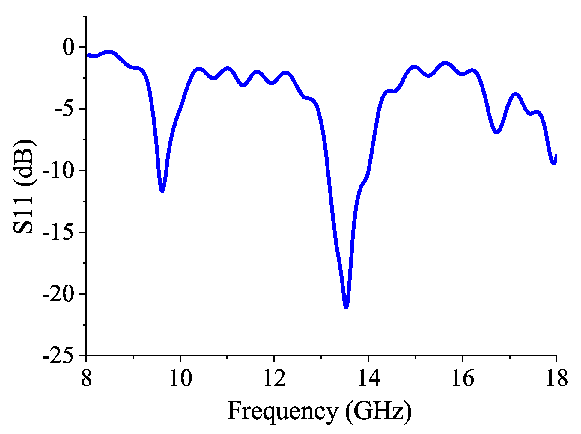
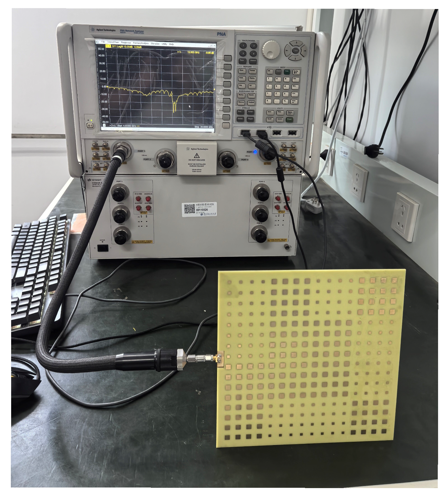
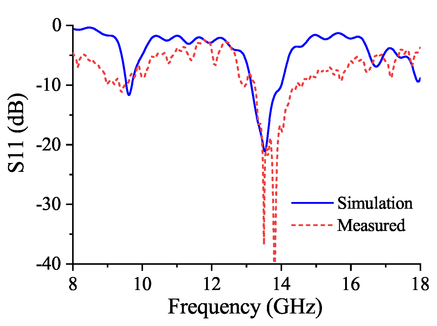
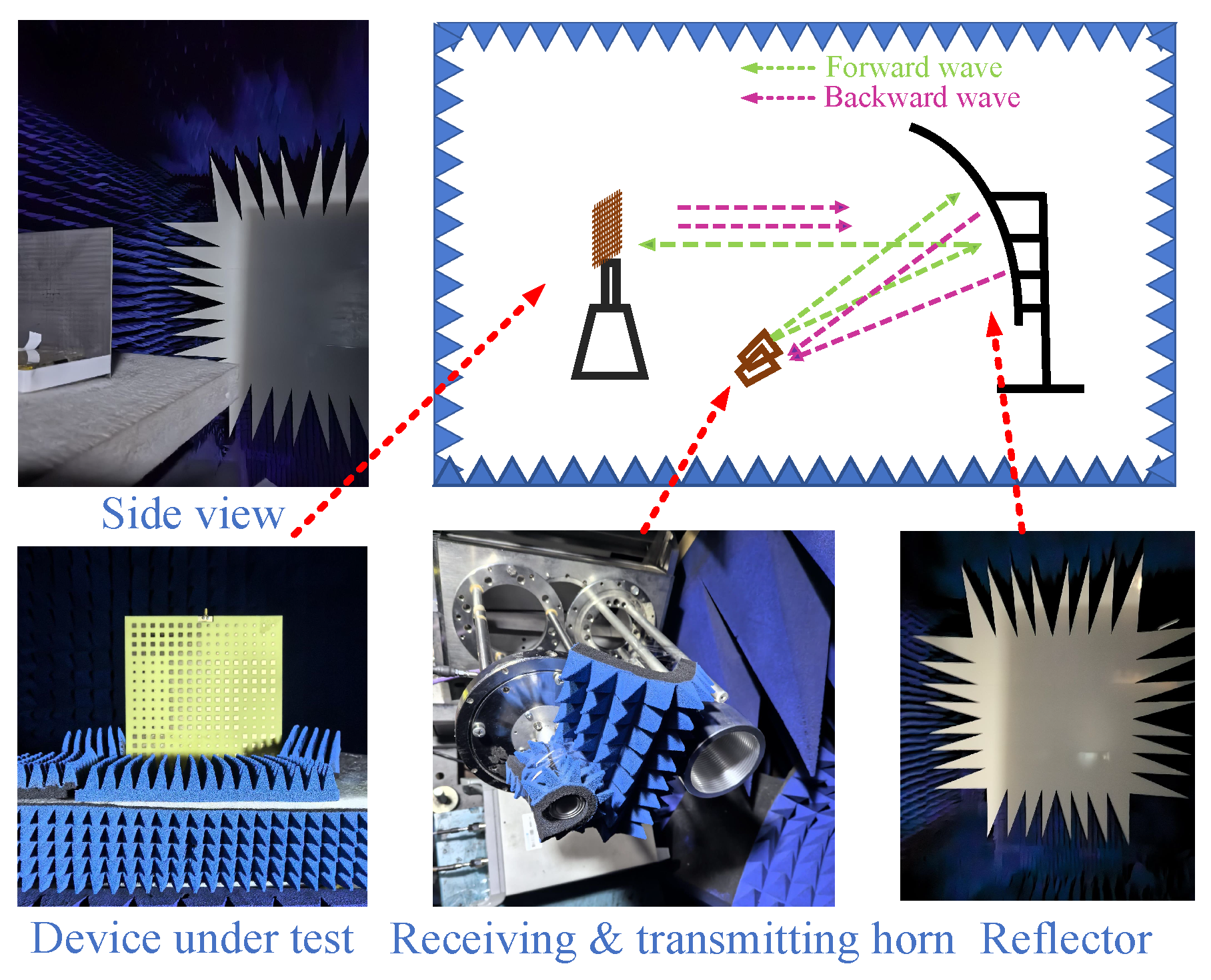
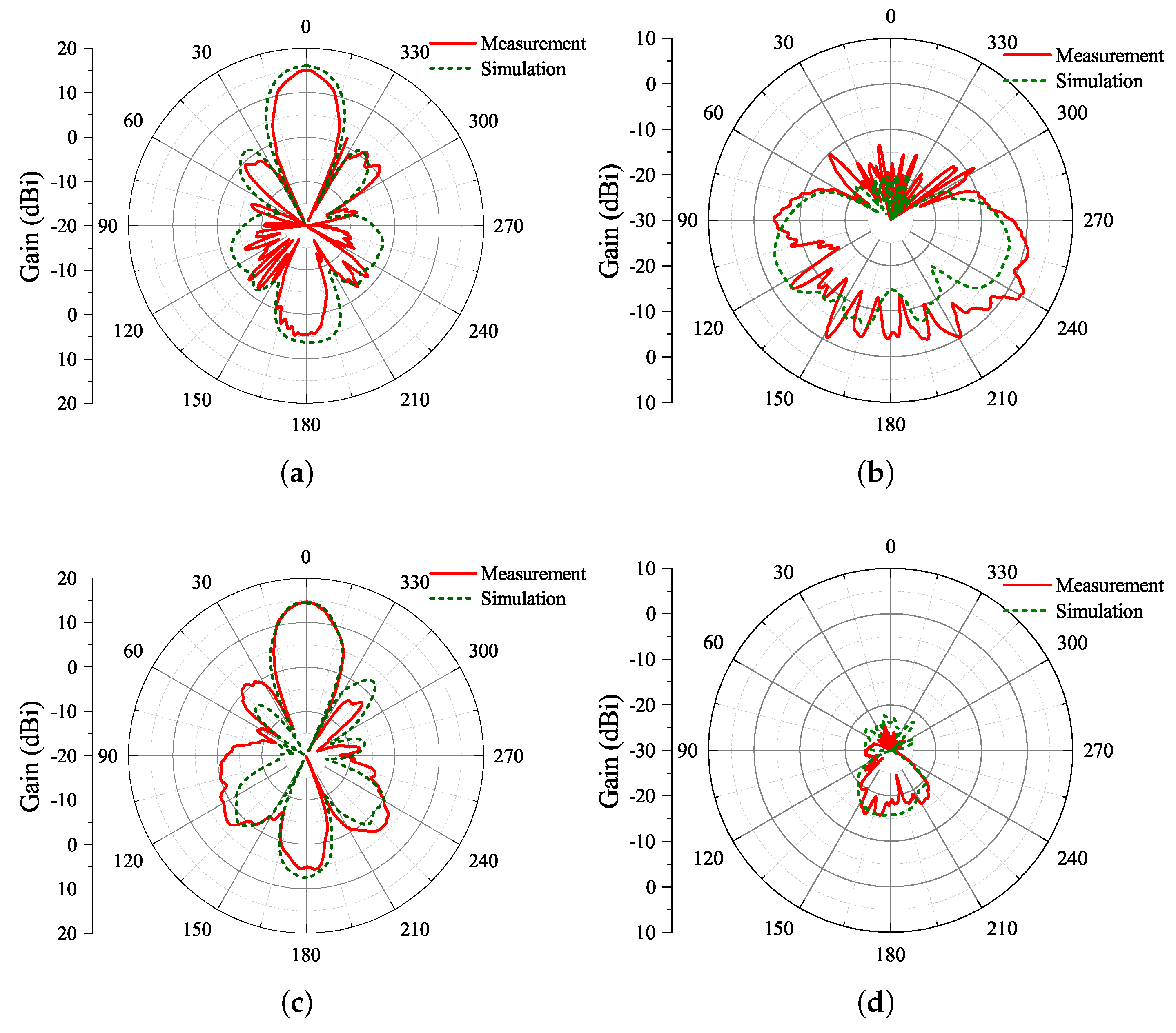
3. Fabrication and Measurement

To verify the results of the co-design, a prototype was manufactured and measured. Figure 12 shows photographs of the the front and back of the fabricated surface. An SMA connector is soldered to the feeding network to connect the coaxial cable.
Figure 13 shows the S-parameter measurement of the feeding network via the vector network analyzer (VNA) PNA-N5247A. As shown in Figure 14, the measured S 11 is less than −10 dB at an operating frequency of 13.5 GHz. The measured S 11 agrees with the simulation results except for a slight frequency shift, which may have been caused by the soldering of the SMA connector. The far-field performance of the array antenna was verified by a far-field test using the compact antenna range technique, and Figure 15 displays the photograph of the anechoic chamber. The signal generated from a signal source is radiated towards the reflector via a standard gain horn antenna, and the array antenna under test is placed at the quiet zone. The measured E-plane pattern and the H-plane pattern are given in Figure 16. As one can see, the measured patterns highly agree with the simulation results. The main-lobes of the E-plane pattern and the H-plane pattern are highly symmetric, and a maximum gain of 14.9 dBi is realized. The side-lobe shows a 10 dB decease and the cross-polarization shows a 20 dB decrease compared with the main-lobe.
Figure 15 gives the RCS measurement of the fabricated bi-functional surface. The original measurement plan involves using dual double-ridged pyramidal horns, which operate in the range of 2 GHz to 18 GHz and have an average gain of 10 dBi, as the receiving antenna and the transmitting antenna in RCS measurement. The under-test surface is placed at the quiet zone, and the double-ridged pyramidal horns are placed parallel to each other at the focus of the reflector, as shown in Figure 15. The forward wave from the transmitting antenna is reflected backward and picked up by the receiving antenna. A metal surface with the same shape is used as the reference plane. The RCS reduction is calculated by making comparisons between the receiving signals from the bi-functional surface and from the reference plane. However, the measured RCS reduction is much lower than the simulation results. This may have been caused by the coupling between the two double-ridged pyramidal horns as they both have wide main-lobe angles. Finally, a modified measurement plan is adopted. A high-directivity corrugated horn with a maximum gain of 23 dBi, 3 dB beam-angle of 13 , and operating band from 12 GHz to 18 GHz is fabricated and used as the transmit antenna, and a circular feeding horn with a corrugated shorting-plane is used as the receiving antenna. The two horns exhibit high directivity, narrow beams, and low side-lobes; thus, the coupling level between the two horns is very low, which ensures an accurate RCS measurement. Figure 17 gives the measured RCS reduction of the bi-functional surface. As one can see, the proposed surface has an average RCS reduction near 10 dB in the range of 12 GHz to 16 GHz. However, it should be noted that the computer numerical control (CNC) fabrication of the corrugated horn is extremely costly. The measurement in the frequency band from 8 GHz to 12 GHz requires another corrugated horn, but due to cost limitations, this measurement was not conducted. Table 2 gives the comparison between our work and the state-of-the-art techniques. Compared with the bi-functional surface based on the PCM technique [12,19,20], the surface proposed in this manuscript exhibits a similar RCS reduction performance. Compared with [21], our work has a narrower bandwidth of RCS reduction. However, the elements in our work based on AMC are highly symmetric and prove to be more convenient for the design of array antennas. Compared with the studies based on the AMC technique [17,18], the proposed bi-functional surface exhibits a wider bandwidth and higher RCS reduction. Compared with the studies based on anisotropic metasurface (AM) [24] and characteristic mode (CM) [25], our work does not need diodes or varactors and exhibits wider bandwidth.

4. Conclusions

This paper proposed a co-design of an RCS-reducing surface and array antenna based on AMC techniques. One kind of AMC is designed with the radiation-scattering function and the other kind of AMC is designed to generate opposed-phased reflections. The proposed co-design strategy guarantees a broad RCS reduction and high-performance array antenna without increasing structural complexity, and it has the potential to be used in large-scale antenna arrays and stealth platforms due to its low cost and high simplicity.

Author Contributions

Conceptualization, X.L. and X.F.; Methodology, R.Y.; Software, R.Y. and Y.W.; Validation, M.W.; Investigation, X.Q.; Data curation, X.Q.; Writing—original draft, R.Y.; Writing—review & editing, X.L.; Visualization, H.Z.; Funding acquisition, X.L. and X.F. All authors have read and agreed to the published version of the manuscript.

Funding

This research was supported in part by the National Natural Science Foundation of China (NSFC) under Grant 62201270 and 62201269 and Natural Science Foundation of Jiangsu Province under Grant BK20220437 and Grant BK20221340.

Data Availability Statement

The original contributions presented in this study are included in the article. Further inquiries can be directed to the corresponding authors.

Conflicts of Interest

The authors declare no conflicts of interest.

References

  1. Knott, E.F.; Shaeffer, J.F.; Tuley, M.T. Radar Cross Section, 2nd ed.; The Institution of Engineering and Technology: London, UK, 2004; pp. 269–295. [Google Scholar]
  2. Chen, H.Y.; Hou, X.Y.; Deng, L.J. Design of frequency-selective surfaces radome for a planar slotted waveguide antenna. IEEE Trans. Antennas Propag. 2009, 8, 1231–1233. [Google Scholar] [CrossRef]
  3. Mei, P.; Lin, X.Q.; Yu, J.W.; Zhang, P.C.; Boukarkar, A. A low radar cross section and low profile antenna co-designed with absorbent frequency selective radome. IEEE Trans. Antennas Propag. 2018, 66, 409–413. [Google Scholar] [CrossRef]
  4. Yang, H.H.; Li, T.; Liao, J.W.; Gao, K.; Li, Q.; Li, S.J.; Cao, X.Y. Ultrawideband low-RCS array antenna based on double-layer polarization conversion metasurface. IEEE Antennas Wirel. Propag. Lett. 2024, 23, 4069–4073. [Google Scholar] [CrossRef]
  5. Xing, Z.; Yang, F.; Yang, P.; Yang, J. A low-RCS and wideband circularly polarized array antenna co-designed with a high-performance AMC-FSS radome. IEEE Antennas Wirel. Propag. Lett. 2022, 21, 1659–1663. [Google Scholar] [CrossRef]
  6. Feresidis, A.P.; Goussetis, G.; Wang, S.H.; Vardaxoglou, J.C. Artificial magnetic conductor surfaces and their application to low-profile high-gain planar antennas. IEEE Antennas Wirel. Propag. 2005, 53, 209–215. [Google Scholar] [CrossRef]
  7. Dewan, R.; Rahim, M.K.A.; Hamid, M.R.; Yusoff, M.F.M.; Samsuri, N.A.; Murad, N.A.; Kamardin, K. Artificial magnetic conductor for various antenna applications: An overview. Int. J. RF Microw. Comput. Aided Eng. 2017, 27, 21105. [Google Scholar] [CrossRef]
  8. Qi, Y.; Zhang, B.; Liu, C.; Deng, X. Ultra-broadband polarization conversion meta-surface and its application in polarization converter and RCS reduction. IEEE Access 2020, 8, 116675–116684. [Google Scholar] [CrossRef]
  9. Zheng, Y.; Gao, J.; Cao, X.; Yuan, Z.; Yang, H. Wideband RCS reduction of a microstrip antenna using artificial magnetic conductor structures. IEEE Antennas Wirel. Propag. Lett. 2015, 14, 1582–1585. [Google Scholar] [CrossRef]
  10. Bandyopadhyay, B.; Bhattacharya, S.; Jaiswal, R.K.; Saikia, M.; Srivastava, K.V. Wideband RCS reduction of a linear patch antenna array using AMC metasurface for stealth applications. IEEE Access 2013, 11, 127458–127467. [Google Scholar] [CrossRef]
  11. Genovesi, S.; Costa, F.; Monorchio, A. Low-profile array with reduced radar cross section by using hybrid frequency selective surfaces. IEEE Trans. Antennas Propag. 2012, 60, 2327–2335. [Google Scholar] [CrossRef]
  12. Zhang, W.; Liu, Y.; Jia, Y. Circularly polarized antenna array with low RCS using metasurface-inspired antenna units. IEEE Antennas Wirel. Propag. Lett. 2019, 18, 1453–1457. [Google Scholar] [CrossRef]
  13. Wang, P.F.; Jia, Y.T.; Hu, W.Y.; Liu, Y.; Lei, H.Y.; Sun, H.B.; Cui, T.J. Circularly polarized polarization conversion metasurface-inspired antenna array with low RCS over a wide band. IEEE Trans. Antennas Propag. 2023, 71, 5626–5636. [Google Scholar] [CrossRef]
  14. Zheng, Q.; Guo, C.; Ding, J.; Vandenbosch, G.A.E. A broadband low-RCS metasurface for CP patch antennas. IEEE Trans. Antennas Propag. 2021, 69, 3529–3534. [Google Scholar] [CrossRef]
  15. Qiu, L.; Xiao, G. A broadband metasurface antenna array with ultrawideband RCS reduction. IEEE Trans. Antennas Propag. 2022, 70, 8620–8625. [Google Scholar] [CrossRef]
  16. Zhang, D.; He, C.; Zhu, Z.; Chen, Q.; Hong, L. An OAM antenna with low RCS characteristic based on radiation-scattering-integration strategy. In Proceedings of the 2023 International Conference on Microwave and Millimeter Wave Technology (ICMMT), Qingdao, China, 14–17 May 2023. [Google Scholar]
  17. Liu, K.Y.; Guo, W.L.; Wang, G.M.; Li, H.P.; Liu, G. A novel broadband bi-functional metasurface for vortex generation and simultaneous RCS reduction. IEEE Access 2018, 6, 63999–64007. [Google Scholar] [CrossRef]
  18. Liu, Y.; Jia, Y.; Zhang, W.; Wang, Y.; Gong, S.; Liao, G. An integrated radiation and scattering performance design method of low-RCS patch antenna array with different antenna elements. IEEE Trans. Antennas Propag. 2019, 67, 6199–6204. [Google Scholar] [CrossRef]
  19. Li, Y.J.; Jin, J.; Yang, Z.G.; Dou, J.; Cheng, H.Y.; Wang, Y.; Yang, H.L. Low-RCS low-profile MIMO antenna and array antenna using a polarization conversion metasurface. Opt. Express 2023, 31, 38771–38785. [Google Scholar] [CrossRef]
  20. Wang, P.; Jia, Y.; Hu, W.; Zhang, J.; Liu, Z.X.; Liu, Y. Broadband low-RCS circularly polarized antenna array with reconfigurable scattering patterns. IEEE Trans. Antennas Propag. 2024, 72, 2279–2290. [Google Scholar] [CrossRef]
  21. Chen, H.Z.; Zhen, Q.T.; Chen, J.; Sun, H.Y.; Li, H.R.; Chernogor, L.F.; Sun, Z.S.; Zheng, Y.; Liu, T.; Jin, Z.J. X-band and low-RCS flexible wideband antenna array based on metasurface. IEEE Antennas Wirel. Propag. Lett. 2025, 24, 567–571. [Google Scholar] [CrossRef]
  22. Constantine, A.B. Antenna Theory: Analysis and Design, 4th ed.; John Wiley & Sons: Hoboken, NJ, USA, 2016; p. 791. [Google Scholar]
  23. Zhao, Y.; Cao, X.; Gao, J.; Liu, X. A low-RCS and high-gain slot antenna using broadband metasurface. IEEE Antennas Wirel. Propag. Lett. 2016, 15, 290–293. [Google Scholar] [CrossRef]
  24. Yang, H.H.; Li, T.; Xu, L.M.; Cao, X.Y.; Jidi, L.; Guo, Z.X. Low in-band-RCS antennas based on anisotropic metasurface using a novel integration method. IEEE Trans. Antennas Propag. 2021, 69, 1239–1248. [Google Scholar] [CrossRef]
  25. Elahi, M.; Koziel, S.; Leifsson, L. A non-PCM-based 2 × 2 MIMO antenna array with low radar cross-section using characteristic mode analysis. IEEE Access 2025, 13, 34296–34306. [Google Scholar] [CrossRef]
Figure 1. The radiation−scattering AMC unit. (a) Geometry. (b) Radiation pattern. Parameters are h = 2.2 mm, W 1 = 5.5 mm, and P = 12 mm.
Electronics 14 02392 g001
Figure 2. (a) The reflection phase of the radiation−scattering AMC and opposed−phase AMC units and (b) the corresponding phase difference.
Electronics 14 02392 g002
Figure 3. The checkerboard configuration of the two sub−arrays. Parameters are W 0 = 3 mm, W 1 = 5.5 mm, P = 12 mm, h = 2.2 mm, W s = 192 mm, and L s = 192 mm.
Electronics 14 02392 g003
Figure 4. The 3D reflection patterns of the proposed bi-functional surface with (a) 2 × 2 sub−array, (b) 4 × 4 sub−array, (c) 8 × 8 sub−array, and (d) the reference plane at 14 GHz.
Electronics 14 02392 g004
Figure 5. The 2D reflection patterns of the proposed bi−functional surface at (a) 10 GHz, (b) 12 GHz, (c) 14 GHz, and (d) 16 GHz.
Electronics 14 02392 g005
Figure 6. Mono−static RCS in normal incident angle.
Electronics 14 02392 g006
Figure 7. Arrangement of array elements.
Electronics 14 02392 g007
Figure 8. The feeding network of the array antenna.
Electronics 14 02392 g008
Figure 9. The S−parameter of the feeding network.
Electronics 14 02392 g009
Figure 10. Overall structure of the bi−functional surface.
Electronics 14 02392 g010
Figure 11. The far−field patterns of the proposed array antenna: (a) E−plane and (b) H−plane.
Electronics 14 02392 g011
Figure 12. The fabricated bi-functional surface: (a) top view and (b) bottom view.
Electronics 14 02392 g012
Figure 13. The S-parameter measurement of the feeding network.
Electronics 14 02392 g013
Figure 14. The measured S−parameter of the feeding network.
Electronics 14 02392 g014
Figure 15. The radiation patterns measurement and RCS measurement using compact antenna range technique.
Electronics 14 02392 g015
Figure 16. The radiation patterns of the proposed bi−functional surface at 13.5 GHz. (a) E-plane co-polarization, (b) E-plane cross−polarization, (c) H−plane co−polarization, and (d) H−plane cross−polarization.
Electronics 14 02392 g016
Figure 17. The measured RCS reduction of the bi−functional surface.
Electronics 14 02392 g017
Table 1. Parameters of the feeding network.
ParameterValueParameterValueParameterValueParameterValue
L 0 98.5 L 1 3 L 2 7.6 L 3 6.0
L 4 6.0 L 5 4.0 R 0 0.4 W 3 0.85
W 2 1.8
Note: Unit is mm.
Table 2. Comparison between relative studies.
Ref.RCS Tech.Antenna Band (GHz)Gain (dBi)Size ( λ 3 )RCS Reduction (GHz)Other
[12]PCM8.2–1212.6 1.88 × 1.88 × 0.1 7.6–16.2/76%/>10 dB
[19]PCM5.63–6.1212–15.6 2.55 × 2.55 × 0.07 8–18/77%/>6 dB
[20]PCM7.7–11.110–12 1.69 × 1.69 × 0.07 8.2–11/29%/>10 dB
[21]PCM8.7–11.510–12 2.2 × 2.2 × 0.1 9.2–21.2/79%/>10 dB
[24]AM2.96–3.0417.7 2.4 × 2.4 × 0.02 3.0–3.15/4.7%/>10 dBwith varactors
[25]CM9.6–10.74–6 1.9 × 1.9 × 0.07 8.5–12/34%/>9 dBwith diodes
[17]AMC4.786 1.59 × 1.59 × 0.05 4.6–6.1/26%/>8 dBOAM
[18]AMC4.8–5.415 2 × 2 × 0.04 4–8/67%/>5 dB
This workAMC13.1–14.115 2.09 × 2.09 × 0.13 10–16/46%/>8 dB
Disclaimer/Publisher’s Note: The statements, opinions and data contained in all publications are solely those of the individual author(s) and contributor(s) and not of MDPI and/or the editor(s). MDPI and/or the editor(s) disclaim responsibility for any injury to people or property resulting from any ideas, methods, instructions or products referred to in the content.

