Article

Theoretical Design and Simulation of a Dual-Band Sheet Beam Extended Interaction Oscillator

1
Key Laboratory of Microwave and Optical Wave Application Technology, Guilin University of Electronic Technology, Guilin 541004, China
2
China Academy of Science & Technology Development Guangxi Branch, Nanning 530022, China
*
Author to whom correspondence should be addressed.
Electronics 2025, 14(5), 966; https://doi.org/10.3390/electronics14050966
Submission received: 16 December 2024 / Revised: 13 February 2025 / Accepted: 25 February 2025 / Published: 28 February 2025
(This article belongs to the Special Issue Broadband High-Power Millimeter-Wave and Terahertz Devices)

Abstract

:
Millimeter-wave devices have great application value and development prospects in military radar, satellite communication, and other fields. Extended interaction devices (EIDs) are widely used in various fields because of their small size, light weight, large bandwidth, and high output power, which are of great significance to the research of millimeter-wave sources. This article presents the design of a sheet beam, dual-beam, dual-cavity coupled extended interaction oscillator (EIO) that can operate separately at 94 GHz and 140 GHz. The coupling coefficient, characteristic impedance, and other parameters were analyzed to optimize the cavity structure and improve transmission performance. The results of the 3D particle-in-cell (PIC) simulation demonstrated that the designed EIO reached a peak output power of 6.3 kW and 41 kW, respectively, when driven by sheet electron beams of 3 A, 34 kV and 3 A, 56 kV.

1. Introduction

Terahertz radiation has shown promising prospects in basic disciplines such as information science, physics, materials science, astronomy, biology, and chemistry. The development of high-power, high-efficiency, broadband, low-cost, and long-life radiation sources in the terahertz frequency band is a crucial aspect of terahertz technology research. Among the various high-frequency radiation sources in this band, electric vacuum devices stand out as the most promising for advancing high-power applications [1,2,3]. The interaction system of the klystron consists of a single-gap resonant cavity and a drift tube, where velocity modulation and density modulation of the electron beam are performed separately, with high output power and gain, but relatively narrow bandwidth [4,5]. The interaction system of traveling wave tubes is a type of slow-wave structure, where velocity modulation and density modulation are performed simultaneously, with a relatively wide bandwidth. However, it is not as ideal in terms of gain and output power. As a new type of vacuum electronic device, EIDs integrate the strengths of both klystrons and traveling wave tubes, providing characteristics like broad bandwidth, high efficiency, and high-power capability [6,7,8]. The beam–wave interaction of EIDs occurs in multiple gaps, allowing them to achieve high characteristic impedance and improve the gain of the cavity. At the same time, the external quality factor of EID structure is smaller, and the Ohmic loss of the cavity is smaller, which can achieve high-power and high-gain output [9,10,11,12]. In addition, the use of a metal structure design is also beneficial for device heat dissipation and processing assembly.
Sheet beam EIO (SBEIO) is used to solve the problem of relatively small electron beam channels caused by high operating frequency, which affect electron beam transmission [13,14]. At the same operating frequency, the sheet beam’s cross-sectional area is larger than that of a traditional pencil electron beam, resulting in an increased beam–wave interaction area and an enhanced power capacity [15]. As described in the aforementioned studies, they are all based on a single operating frequency band, achieving excellent performance such as high power or wide bandwidth within a single band. However, utilizing two coupled extended interaction circuits to achieve dual-band operation is highly beneficial for expanding the application scope of EIOs, as well as reducing manufacturing complexity and cost.
Compared with traditional structures, this structure achieved effective connection and energy output by coupling two adjacent circuits through the same coupling slot. The structure of this article is organized as follows: In Section 2, the physical model of EIO interaction is designed and optimized. In Section 3, PIC simulations are conducted, and the results are analyzed. Finally, conclusions are drawn in Section 4.

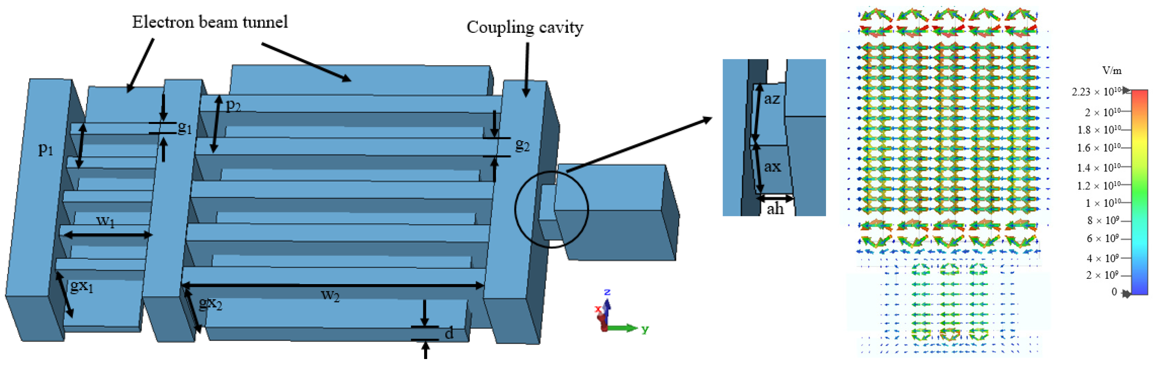
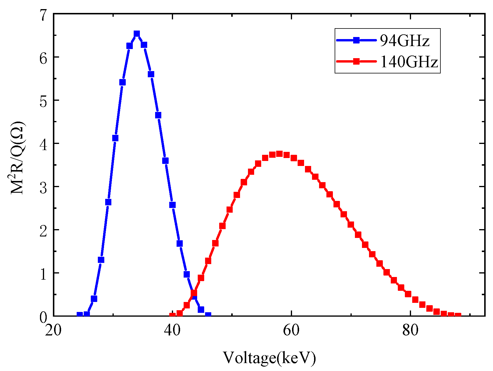
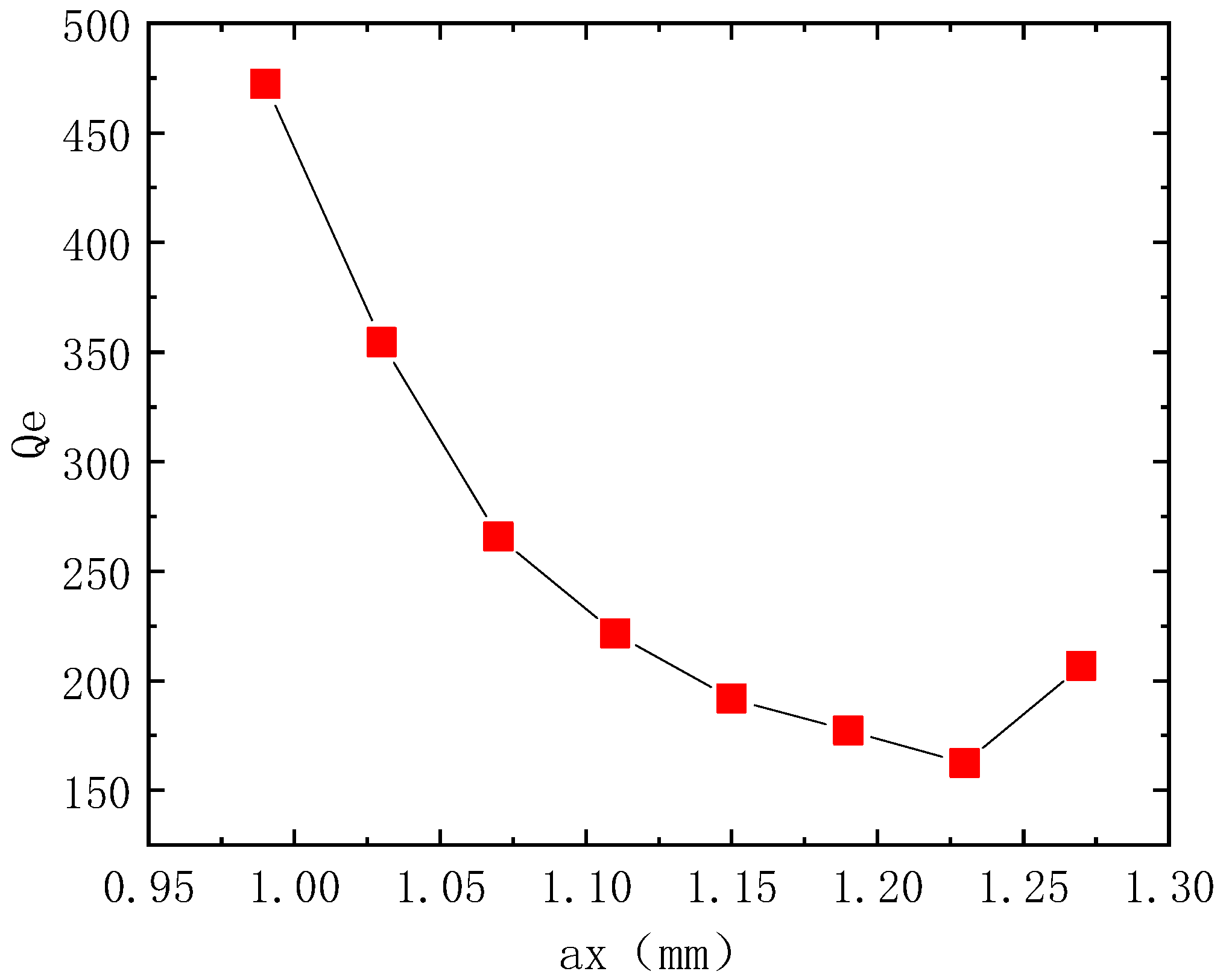
2. Physical Model Analysis

The high-frequency structure of the EIO consists of coupling slots, multiple gaps, and an electron beam channel. This study proposes an EIO dual-cavity coupled high-frequency structure with five gaps, and its electric field distribution is shown in Figure 1, consisting of a coupling cavity shared by one EIO operating at 94 GHz and 140 GHz.
A sheet electron beam is used to minimize space charge effects and reduce the need for a focused magnetic field, while simultaneously expanding the interaction area between the electron beam and the electric field, thus enhancing circuit efficiency. The coupling slots on both sides of the high-frequency gap couple the longitudinal electric field of the gaps and effectively modulate the electron beam. The dimensions of the EIO are provided in Table 1.
The electrons in the resonant cavity move along the electron beam channel towards the z-axis direction and are constrained by a uniform magnetic field of 0.5 T. The background material is set to copper with a conductivity of 2.8 × 10⁷ S/m [16].
The operating mode of the EIO in this work is the 2π mode. Compared to the π mode, the 2π mode offers a higher characteristic impedance than the π mode, which contributes to enhancing electron efficiency and output power [17]. The TM11 mode is characterized by the strongest electric field component along the propagation direction of the electron beam at high frequencies. Therefore, the TM11-2π mode was chosen as the operating mode of the EIO in this study.
Additionally, the larger structure size associated with this mode makes it easier to manufacture. The period of the resonant cavity can be calculated by the following formula [18,19]:
β e p = m π
while
β e = ω v 0
v 0 = c 1 1 1 + U 511 2 ,
where v 0 is the electron beam velocity and U is operating voltage.
The coupling coefficient M is used to characterize the degree of modulation experienced by the electron beam, which is defined as the ratio of the modulation voltage applied to the electron beam to the actual modulation voltage across the gap. The efficiency of the interaction between the electron beam and the electric field is described as characteristic impedance R / Q [20]. Their expressions are given as follows:
M = + f z e j β e z d z + f z d z
R / Q = V m 2 ω 0 W s = a b E d l 2 ω 0 V E 2 d V
where E is the axial electric field, ω is the resonant angular frequency,   f z is the normalized field distribution function, V m is the amplitude of the gap electric field, and W s is the energy stored in the gap. The effective characteristic impedance M 2 R / Q is used to evaluate beam–wave interaction as the interaction strength between the characteristic impedance and coupling coefficient. The M 2 R / Q variation versus voltage is shown in Figure 2. From this, it can be seen that 94 GHz and 140 GHz obtain the maximum effective characteristic impedance at operating voltages of 34 kV and 56 kV, respectively.
For the 2π mode, its cutoff frequency is mainly determined by gx [21]. As shown in Figure 3, with other parameters held constant, the resonant frequency of the gap corresponds to different gx variations, and with increasing gx, the resonant frequency decreases, and the characteristic impedance gradually reaches a certain optimal value. Therefore, the operating frequency can be significantly adjusted during the design process by adjusting the gap narrow edge size gx.
The performance of the output-coupled structure affects the energy output of the cavity structure. In order to efficiently couple the energy output, it is necessary to connect the rectangular waveguide and the resonant cavity through a coupling slot. In this study, the period length of the resonant cavity is 0.92 mm. According to the standing wave half-wavelength, the longitudinal dimension az of the coupling slot is designed to be 0.8 mm, and ay is set as 0.4 mm.
Q e is a parameter that measures the transmission capacity of the output structure and characterizes the coupling between the circuit and the external load. Q e is defined as follows:
Q e = ω 0 τ 4 = 2 π f τ 4
where τ is group delay time, ω 0 is the resonant angular frequency, and f is the operating frequency. A larger Q e indicates a higher energy storage in the cavity and a smaller output power from the circuit. Conversely, more energy from the cavity can be coupled into the output circuit when Q e is smaller. The effect of the change in the lateral dimension ax of the coupling slot on the Q e of the interaction cavity’s 2π mode is shown in Figure 4. When ax increases from 0.98 mm to 1.28 mm, Qe decreases from its maximum value, indicating that the output power will increase with the increase in ax. Microwave energy will be better output to the coupling structure, and the maximum output power will be reached when ax is 1.22 mm. Ultimately, ax is chosen as 1.22 mm as the lateral dimension of the coupling slot to maximize the output power of the circuit.

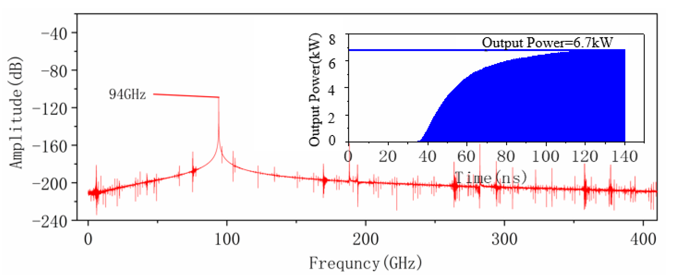
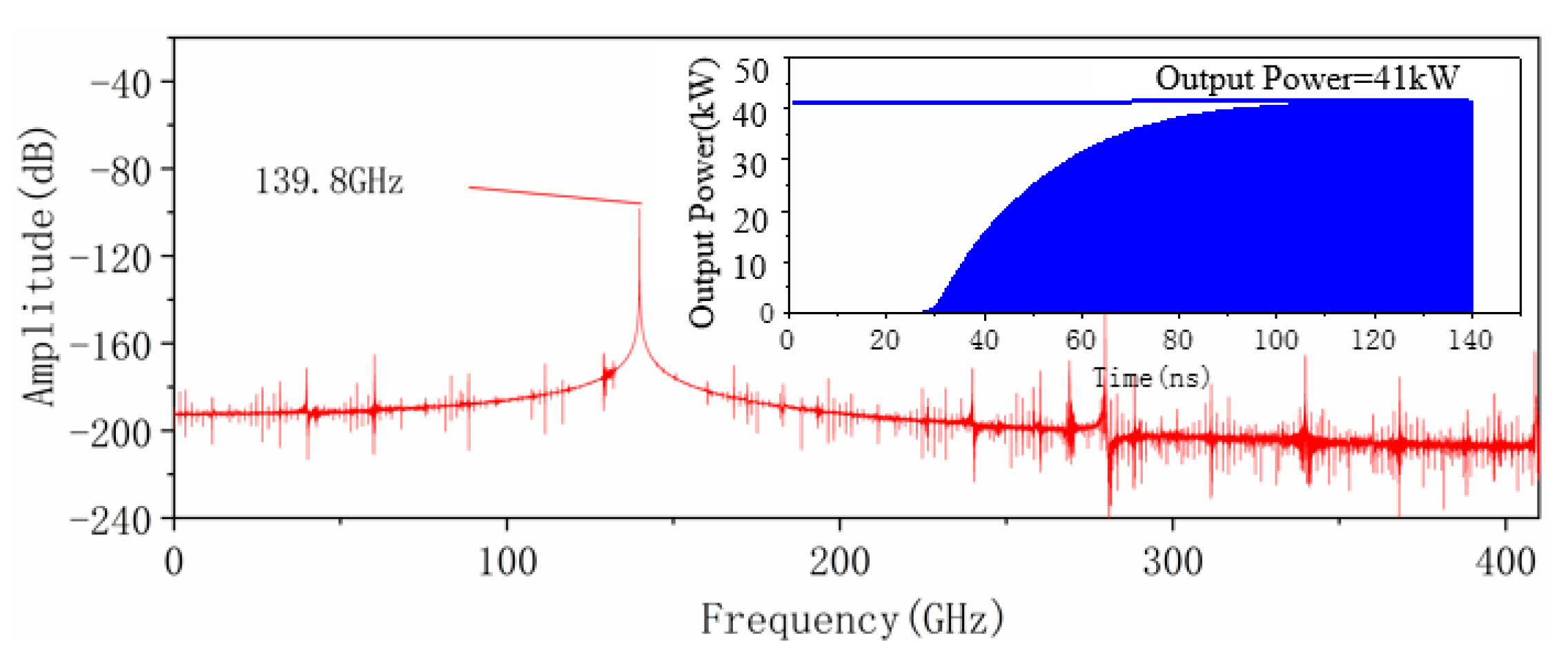
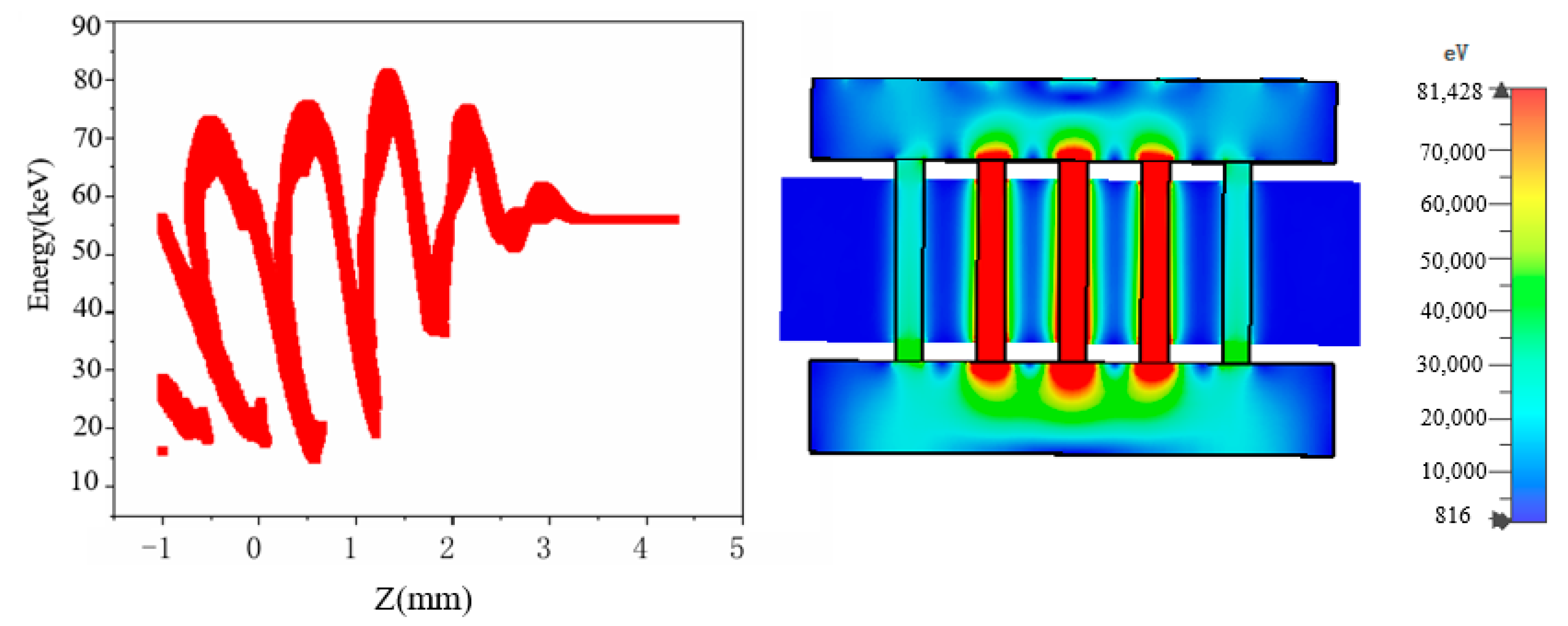
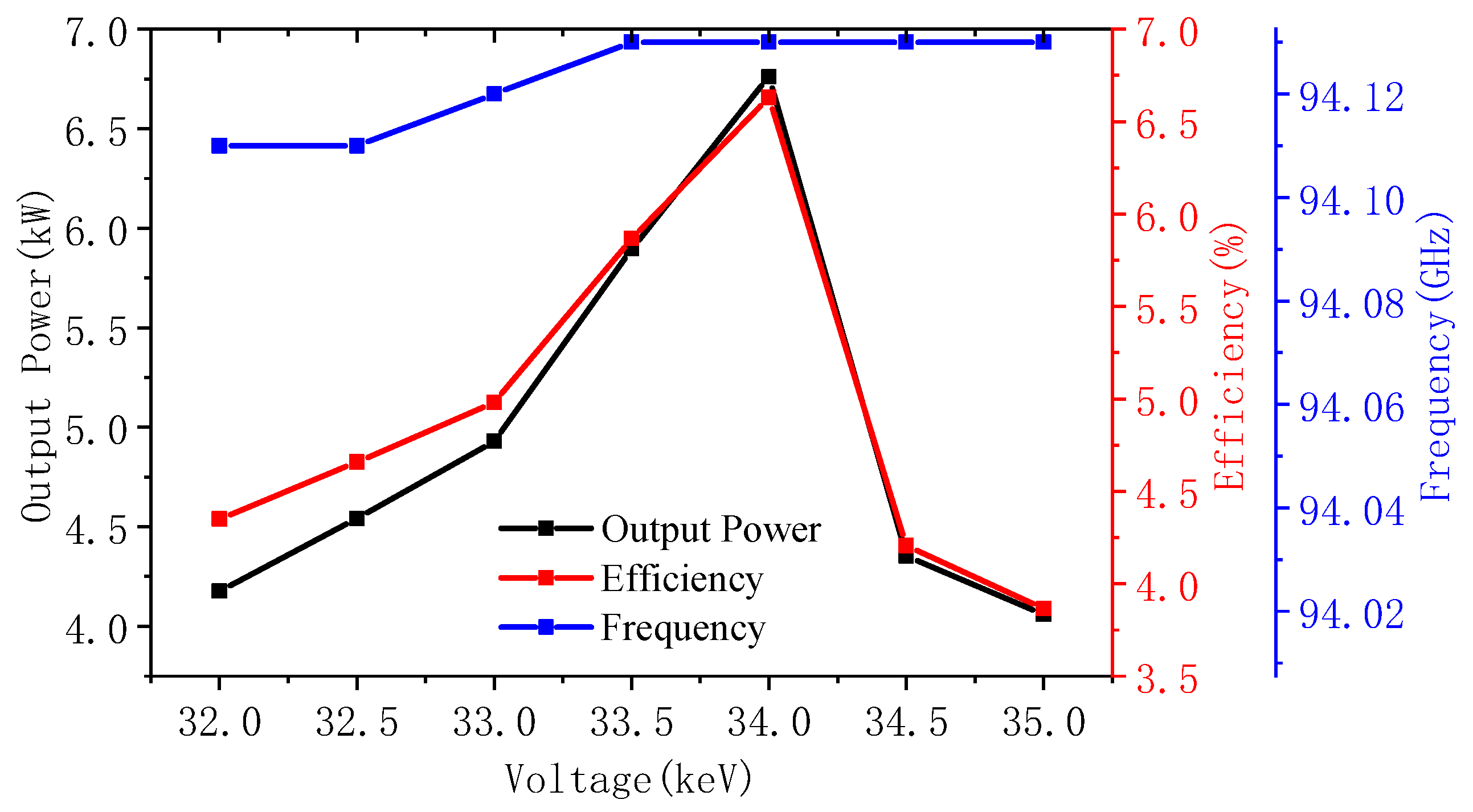
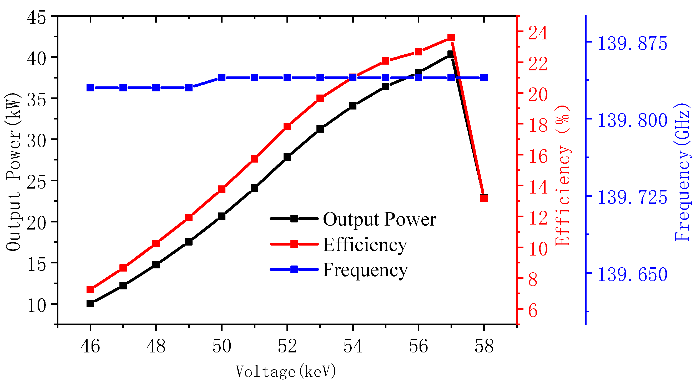
3. PIC Simulation and Analysis

A dual-beam, dual-frequency EIO hot test model was established using simulation software CST studio and is being researched for its beam–wave interaction using particle-in-cell (PIC) simulation. Taking into account machining precision and ohmic losses, the metal material is set to copper with a conductivity of 2.8 × 10⁷ S/m. To simplify the simulation model, the cathode emission surface was simplified as a rectangular metallic object, and a DC emission mode is used with an electron beam size of 5 × 0.5 mm and an injection current of 3 A at a voltage of 34 kV at 94 GHz; at 140 GHz, the dimensions were 1.5 × 0.2 mm, with an injection current of 3 A and a voltage of 56 kV.
Due to the structural characteristics of the dual-electron-beam channel, in addition to the co-directional emission of electron beams used in this study, counter-directional emission can also be adopted. Regardless of the emission method, the dual electron beams are effectively modulated within the interaction cavity, achieving the bunching phenomenon. The following Figure 5 presents the particle simulation results for both emission methods.
The key difference between the two lies in their transmission directions: in the co-directional emission, both electron beams travel along the +z direction, are continuously modulated, and achieve effective bunching at the end of the circuit, converting their energy into high-frequency field energy. In the counter-directional emission, the electron beams travel along the +z and −z directions, respectively, and are modulated along their respective transmission paths. Effective bunching occurs at the front and end of the circuit, where energy is then converted into high-frequency field energy.
Additionally, the counter-directional emission poses a greater challenge to the pre-stage electron optical system due to the opposite emission directions of the electron beams. However, regardless of the position in the circuit where the electron beams transfer their energy to the high-frequency field, the electromagnetic field working in the cavity as a whole is ultimately amplified.
The output power signals of EIO operating independently at 94 GHz and 140 GHz are shown in the inset of Figure 6 and Figure 7, with the signal stabilizing and amplifying within 140 ns. The corresponding spectrum graph is shown, where the output signal spectrum is clean, with no competing mode spectra observed.
Figure 8 and Figure 9 show the electron energy distribution of electron bunching and the energy of the sheet beam along the z direction at the 60 ns. It can be seen that in the latter part of the EIO, the modulated electron beam experiences a decrease in electron velocity, resulting in bunching, and releasing energy. The electron bunching diagram shows that the electrons are well modulated as they travel within the cavity, indicating good beam–wave interaction. From the electric field distribution diagram, it can be seen that in the interaction gap, the electric field distribution within the electron beam channel is fairly uniform.
The curves of the circuit output characteristics as a function of voltage are shown in Figure 10 and Figure 11. The 94 GHz and 140 GHz electron beams can both operate stably within voltage ranges of 32–35 kV and 46–58 kV, respectively. Simulation results indicate that the output power of the interaction circuit generally increases with the increase in beam voltage. Specifically, the 94 GHz circuit output power increases from 4.1 kW to 6.7 kW, and the beam–wave interaction efficiency rises from 3.8% to 6.6%. For the 140 GHz circuit, the output power increases from 10 kW to 42 kW, and the beam–wave interaction efficiency increases from 7.2% to 23%. The output frequency remains almost unchanged and operates stably at the designed frequency point.

4. Conclusions

In summary, this study presented a novel design for a high-frequency sheet beam dual-cavity coupled EIO that operated at the dual frequencies of 94 GHz and 140 GHz. The dual-frequency operation is achieved through coupling two extended interaction circuits with a common coupling cavity, with output power delivered through a standard rectangular waveguide. Under different electron injection conditions of 3 A at 34 kV and 3 A at 56 kV, the circuit demonstrated stable output powers of 6 kW at 94 GHz and 42 kW at 140 GHz, respectively.
This dual-frequency design significantly broadened the potential application of EIO technology by enabling operation at two distinct frequency bands. Additionally, the use of a sheet beam to increase the cross-sectional area of the electron beam not only enhances power efficiency but also provides a practical solution for scaling up the output power of the oscillator.
Compared to traditional single-frequency extended interaction circuits, the dual-frequency EIO proposed in this study enables high power output at two distinct frequency bands, offering new possibilities for practical applications in millimeter-wave and terahertz technologies. This design, especially when operating at higher frequencies, increases the power capacity of the EIO and provides new insights for the design of multi-frequency and dual-frequency EIO circuits. This work addressed the limitations of traditional single-frequency EIOs in terms of bandwidth and high power output.
This dual-frequency EIO design opens new avenues for high-power, broadband applications, particularly in the millimeter-wave and terahertz frequency ranges, and serves as a foundation for future research on multi-frequency, multi-mode EIO circuits. It highlights the importance of optimizing circuit design and electron beam parameters to achieve reliable, high-power output across multiple frequency bands, addressing the limitations found in previous single-band EIO configurations.

Author Contributions

Conceptualization, J.L. and Q.Z.; methodology, J.L.; resources, X.L. (Xiaofeng Li), X.L. (Xingpeng Liu), Q.Z., R.L. and S.S.; data curation, Q.Z.; formal analysis, Q.Z. and X.L. (Xiaofeng Li); writing—original draft preparation, J.L. and Q.Z.; writing—review and editing, Q.Z. and S.S.; funding acquisition, Q.Z. All authors have read and agreed to the published version of the manuscript.

Funding

This work is supported in part by the Natural Science Foundation Project 62361019, 62001131, the Guangxi Natural Science Foundation 2024GXNSFAA010502, the Dean Project of Guangxi Key Laboratory of Wireless Broadband Communication and Signal Processing Grant Nos: GXKL06190102, Guangxi, and the major special project plan of Guilin City in 2022, fund number 20220101.

Data Availability Statement

Data are within the article.

Conflicts of Interest

The authors declare no conflict of interest.

References

  1. Tucek, J.C.; Basten, M.A.; Gallagher, D.A.; Kreischer, K.E. Operation of a compact 1.03 THz power amplifier. In Proceedings of the IEEE International Vacuum Electronics Conference, Monterey, CA, USA, 24–26 April 2018; pp. 1–2. [Google Scholar]
  2. Wang, Z.; Qu, Z.; Li, L.; Shang, X.; Cao, L.; Tang, B.; Xiao, L. Investigation on a broadband 220 GHz extended interaction klystron. In Proceedings of the IEEE International Vacuum Electronics Conference, Busan, Republic of Korea, 28 April–1 May 2019; pp. 1–2. [Google Scholar]
  3. Bi, L.; Meng, L.; Yin, Y.; Xu, C.; Zhu, S.; Peng, R.; Zeng, F.; Chang, Z.; Wang, B.; Li, H.; et al. Design and Analysis of a High-Order Mode Ladder-Type RF Circuit for Stable Operation in a W-Band Extended Interaction Oscillator. IEEE Trans. Electron Devices 2019, 66, 729–735. [Google Scholar] [CrossRef]
  4. Berry, D.; Deng, H.; Dobbs, R.; Horoyski, P.; Hyttinen, M.; Kingsmill, A.; MacHattie, R.; Roitman, A.; Sokol, E.; Steer, B. Practical aspects of EIK technology. IEEE Trans. Electron Devices 2014, 61, 1830–1835. [Google Scholar] [CrossRef]
  5. Shu, G.X.; Wang, J.; Qian, Z. Study of Performance Improvement for a Q-Band Sheet-Beam Traveling-Wave Tube. IEEE Trans. Electron Devices 2018, 65, 3970–3975. [Google Scholar] [CrossRef]
  6. Steer, B.; Roitman, A.; Horoyski, P.; Hyttinen, M.; Dobbs, R.; Berry, D. Advantages of extended interaction klystron technology at millimeter and sub-millimeter frequencies. In Proceedings of the 2007 16th IEEE International Pulsed Power Conference, Albuquerque, NM, USA, 17–22 June 2007; Volume 2, pp. 1049–1053. [Google Scholar]
  7. Poseur, J.; Wright, E.; Nguyen, K.T.; Balkcum, A.; Wood, F.N.; Myers, R.E.; Levush, B. Demonstration of a multikilowatt, solenoidally focused sheet beam amplifier at 94 GHz. IEEE Trans. Electron Devices 2014, 61, 1630–1636. [Google Scholar] [CrossRef]
  8. Pasour, J.; Nguyen, K.T.; Wright, E.; Pershing, D.; Abe, D.; Balkcum, A.; Wood, F.; Myers, R.; Cook, A.; Hanna, J.; et al. High-power mm W sheet beam amplifiers. In Proceedings of the 16th IEEE International Vacuum Electronics Conference, Beijing, China, 27–29 April 2015; pp. 1–2. [Google Scholar]
  9. Booske, J.H.; Dobbs, R.J.; Joye, C.D.; Kory, C.L.; Neil, G.R.; Park, G.S.; Park, J.; Temkin, R.J. Vacuum electronic high power terahertz sources. IEEE Trans. THz Sci. Technol. 2011, 1, 54–75. [Google Scholar] [CrossRef]
  10. Chang, Z.W.; Meng, L.; Yin, Y.; Wang, B.; Li, H.; Bi, L.; Peng, R.; Xu, C. Study of a dual-mode W-band extended interaction oscillator. IEEE Trans. Electron Devices 2018, 65, 2620–2625. [Google Scholar] [CrossRef]
  11. Shu, G.X.; Yin, Y.; Zhang, L.; Zhao, J.P.; Liu, G.; Phelps, A.D.R.; Cross, A.W.; He, W. Demonstration of a planar W-Band, kW-level extended interaction oscillator based on a pseudospark-sourced sheet electron beam. IEEE Electron Device Lett. 2018, 39, 432–435. [Google Scholar] [CrossRef]
  12. Chen, S.Y.; Liu, J.Q.; Shui, Y.T.; Gao, L.; Jiang, Z.; Bai, J.; Liu, H.; Liu, X.; Zhang, X.; Xu, F.; et al. Design and particle-in-cell simulation of sub-THz sheet beam EIK. In Proceedings of the 41st International Conference Infrared, Millimeter, and Terahertz Waves (IRMMW-THz), Copenhagen, Denmark, 25–30 September 2016; pp. 1–2. [Google Scholar]
  13. Pasour, J.; Nguyen, K.; Wright, E.; Balkcum, A.; Atkinson, J.; Cusick, M.; Levush, B. Demonstration of a 100-kW Solenoidally Focused Sheet Electron Beam for Millimeter-Wave Amplifiers. IEEE Trans. Electron Devices 2011, 58, 1792–1797. [Google Scholar] [CrossRef]
  14. Soltani, H.B.; Abiri, H. Developing a load-line concept to study the extended interaction oscillators. IEEE Trans. Electron Devices 2017, 64, 3429–3436. [Google Scholar] [CrossRef]
  15. Wang, J.X.; Barnett, L.R.; Luhmann, N.C.; Shin, Y.M.; Humphries, S. Electron beam transport analysis of W-band sheet beam klystron. Phys. Plasma 2010, 17, 043111. [Google Scholar] [CrossRef]
  16. Xu, X.T.; Yuan, X.S.; Li, H.L.; Chen, Q.; Zu, Y.; Cole, M.; Xie, J.; Yin, Y.; Yan, Y. Design of a G-Band Extended Interaction Klystron Based on a Three-Coupling-Hole Structure. IEEE Trans. Electron Devices 2022, 69, 1368–1373. [Google Scholar] [CrossRef]
  17. Ren, X.X.; Wang, J.X.; Dong, K.; Liu, G.; Shu, G.; Fu, H.; Balfour, E.A. Study of a High-Efficiency 34-GHz Sheet Beam Extended Interaction Oscillator with Low Filling Factor. IEEE Trans. Electron Devices 2016, 63, 4074–4080. [Google Scholar]
  18. Zhang, F.Y.; Liu, W.X.; Jin, Z.H.; Zhang, Z.; Zhang, Z.; Zhao, K.; Xu, J.; Wei, Y.; Lan, F.; Yang, Z. Design and Simulation for 100-Watt-Class 340-GHz Extended Interaction Klystron. IEEE Trans. Electron Devices 2022, 69, 6329–6335. [Google Scholar] [CrossRef]
  19. Li, R.; Ruan, C.; Zhang, H.; ul Haq, T.; He, Y.; Shan, S. Theoretical Design and Numerical Simulation of Beam-Wave Interaction for G-Band Unequal-Length Slots EIK with Rectangular Electron Beam. IEEE Trans. Electron Devices 2018, 65, 3500–3506. [Google Scholar] [CrossRef]
  20. Chodorow, M.; Wessel-Berg, T. A high-efficiency klystron with distributed interaction. IRE Trans. Electron Devices 1961, 8, 44–55. [Google Scholar] [CrossRef]
  21. Jabotinski, V.; Chernin, C.; Nguyen, K.T.; Antonsen, T.M.; Levush, B. Nonperiodic Perturbations in Periodic RF Structures. IEEE Trans. Microw. Theory Tech. 2012, 60, 915–929. [Google Scholar] [CrossRef]
Figure 1. Physical model of the resonant cavity.
Electronics 14 00966 g001
Figure 2. M 2 R / Q   variation in the EIO.
Electronics 14 00966 g002
Figure 3. The influence of gx variations on operating frequency and R/Q.
Electronics 14 00966 g003
Figure 4. The Q e of 2π mode with different values of the coupling slot ax.
Electronics 14 00966 g004
Figure 5. Output signal of (a) co-direction emission and (b) counter-direction emission.
Electronics 14 00966 g005
Figure 6. Output power and spectral analysis at 94 GHz.
Electronics 14 00966 g006
Figure 7. Output power and spectral analysis at 140 GHz.
Electronics 14 00966 g007
Figure 8. The electron energy distribution along the z-axis diagram and electric field contour distribution at 140 GHz.
Electronics 14 00966 g008
Figure 9. The electron energy distribution along the z-axis diagram and electric field contour distribution at 94 GHz.
Electronics 14 00966 g009
Figure 10. Output power, efficiency, and frequency versus voltage at 94 GHz.
Electronics 14 00966 g010
Figure 11. Output power, efficiency, and frequency versus voltage at 140 GHz.
Electronics 14 00966 g011
Table 1. Size of cavity.
SymbolValue (mm)
p 1 0.73
p 2 0.92
g 1 0.25
g 2 0.35
w 1 1.85
w 2 5.8
g x 1 1.12
g x 2 1.76
d 0.5
Disclaimer/Publisher’s Note: The statements, opinions and data contained in all publications are solely those of the individual author(s) and contributor(s) and not of MDPI and/or the editor(s). MDPI and/or the editor(s) disclaim responsibility for any injury to people or property resulting from any ideas, methods, instructions or products referred to in the content.

