Article

An Ultra-Wideband Low-Noise Amplifier with a New Cross-Coupling Noise-Canceling Technique for 28 nm CMOS Technology

School of Microelectronics, Tianjin University, Tianjin 300072, China
*
Author to whom correspondence should be addressed.
Electronics 2025, 14(10), 1904; https://doi.org/10.3390/electronics14101904
Submission received: 13 April 2025 / Revised: 1 May 2025 / Accepted: 6 May 2025 / Published: 8 May 2025
(This article belongs to the Section Microelectronics)

Abstract

:
This paper presents an ultra-wideband low-noise amplifier (LNA) with a new cross-coupling noise-canceling technique for 28 nm CMOS technology. The entire LNA contains two stages. The first stage employs inductively coupled Gm-boosted technology, while the second stage is a novel asymmetric cross-coupling noise-canceling structure (ACCNCS). Through the introduction of these two key techniques, the LNA achieves balanced performance across a relative bandwidth of 56%. Input/output/inter-stage impedance matching uses a transformer-based network with series-parallel combinations of inductors and capacitors. The LNA is designed in a 28 nm CMOS process with a chip core area of 335 × 665 µm2. The operating frequency range is 26–46 GHz. Post-layout simulation results show that the peak gain of the LNA is 12.6 dB, and the noise figure is between 2.9 and 4.2 dB across the wideband range. At a center frequency of 36 GHz with a supply voltage (VDD) of 0.9 V, the input 1 dB compression point (IP1dB) is −7.6 dBm, while the power consumption is 22 mW.

1. Introduction

In recent years, with the rapid development of mobile internet and the widespread adoption of wireless communication devices, the demand for higher data transmission rates in wireless communication systems has been continuously increasing. The underutilized 5G millimeter-wave frequency band has gradually been recognized as an important solution to address the scarcity of low-frequency resources. Therefore, an increasing proportion of research focus has shifted toward millimeter-wave frequency. The low-noise amplifier (LNA) is a crucial part in the front end of millimeter-wave phased-array receivers, and its noise performance often determines key indicators such as the noise of the subsequent stages and the overall sensitivity of the receiver. On the other hand, the increasingly widespread application scenarios and the growing demand for transmission stability have made the operational bandwidth an important consideration for LNA design. As a result, wideband LNAs have gradually become a research focus. However, the strict requirements for noise, gain flatness, and input matching make it difficult to design an LNA with a matching network that fulfills these requirements. Maintaining such matching performance while operating over a wide bandwidth remains a significant challenge.
Different LNA architectures have different features and characteristics. Compared to traditional common-source (CS) LNAs [1], common-gate (CG) LNAs [2,3,4], cascode (CS-CG) LNAs [5,6], or resistive shunt-feedback LNAs [7], noise-canceling LNAs [8,9,10,11] offer the advantage of canceling channel thermal noise without affecting other circuit performances; hence, this structure has been widely adopted. However, operating in a wide frequency range for 5G millimeter-wave communication still makes it very challenging to achieve a good balance among noise, gain, and input matching. Refs. [12,13] achieved good noise performance and high gain through advanced techniques. However, their operating bandwidths are limited, making them unsuitable for ultra-wideband operation. In contrast, ref. [14] extended the relative bandwidth to 59%, but the result required huge power consumption, which is a luxury in millimeter-wave applications, and its noise figure could not be maintained at a low level. The introduction of a Gm-boosted cross-coupling structure alters the original relationship between impedance and noise, effectively adding adjustable variables, which makes it possible to achieve an impedance that better satisfies performance requirements.
In this paper, an LNA with a new noise-canceling architecture is proposed. Inductive coupling is used at the input stage, and capacitive cross-coupling is employed at the second stage. The two noise-canceling paths are similar to a differential structure, which enables the implementation of capacitive cross-coupling. The circuit is designed using a 28 nm CMOS process, achieving a relatively good balance between gain, noise, linearity, and power consumption. The LNA provides an ultra-wideband operating range of 20 GHz and a fractional bandwidth (FBW) of 56%.
The structure of this paper is as follows: Section 2 discusses the principle and the analysis of key techniques implemented in the proposed LNA. Section 3 provides a detailed explanation of the LNA design methodology, outlining the step-by-step development process, including the design considerations for the transformer components. Section 4 presents the simulation outcomes to validate the proposed design, while Section 5 concludes the paper with a summary of the performance of the proposed LNA.

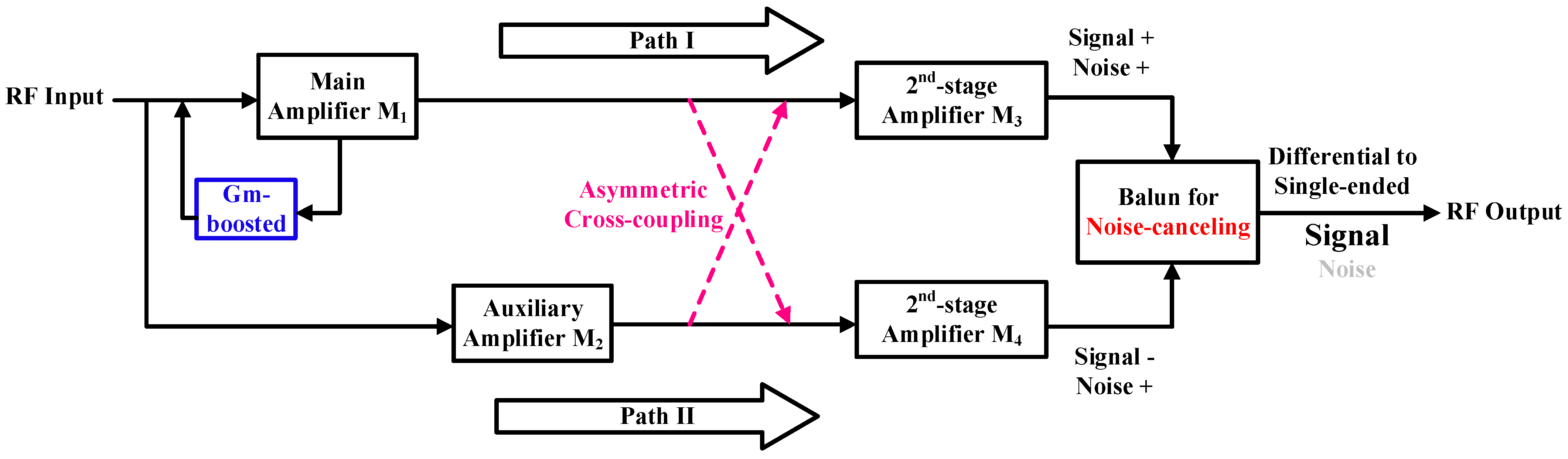
2. Principle of the Proposed LNA

The configuration of the proposed LNA is illustrated in Figure 1. The input RF signal is applied in a single-ended form and is simultaneously fed to the main amplifier M1 in the first stage and the auxiliary amplifier M2 along Path II. These two paths extend from the input to the two second-stage amplifiers and form the dual paths required for noise cancelation. At the output, the voltage signals from the two second-stage amplifiers are combined as differential input, while the in-phase noise components are canceled as part of the common-mode response. This differential output is converted back to a single-ended signal by an output balun, thus enabling a single-ended input and single-ended output LNA configuration. In this proposed LNA configuration, the first stage employs a Gm-boosted structure to enhance the effective transconductance of the main amplifier M1, and its noise contribution is reduced as a result. The second stage introduces an asymmetric cross-coupling structure, which makes the noise cancellation between the two signal paths better meet the design requirements. This cross-coupling structure also optimizes the matching process to achieve better minimum noise matching, maximum gain matching, and conjugate matching of the LNA. After a more effective trade-off among critical metrics, the LNA achieves preferable performance under ultra-wideband conditions.

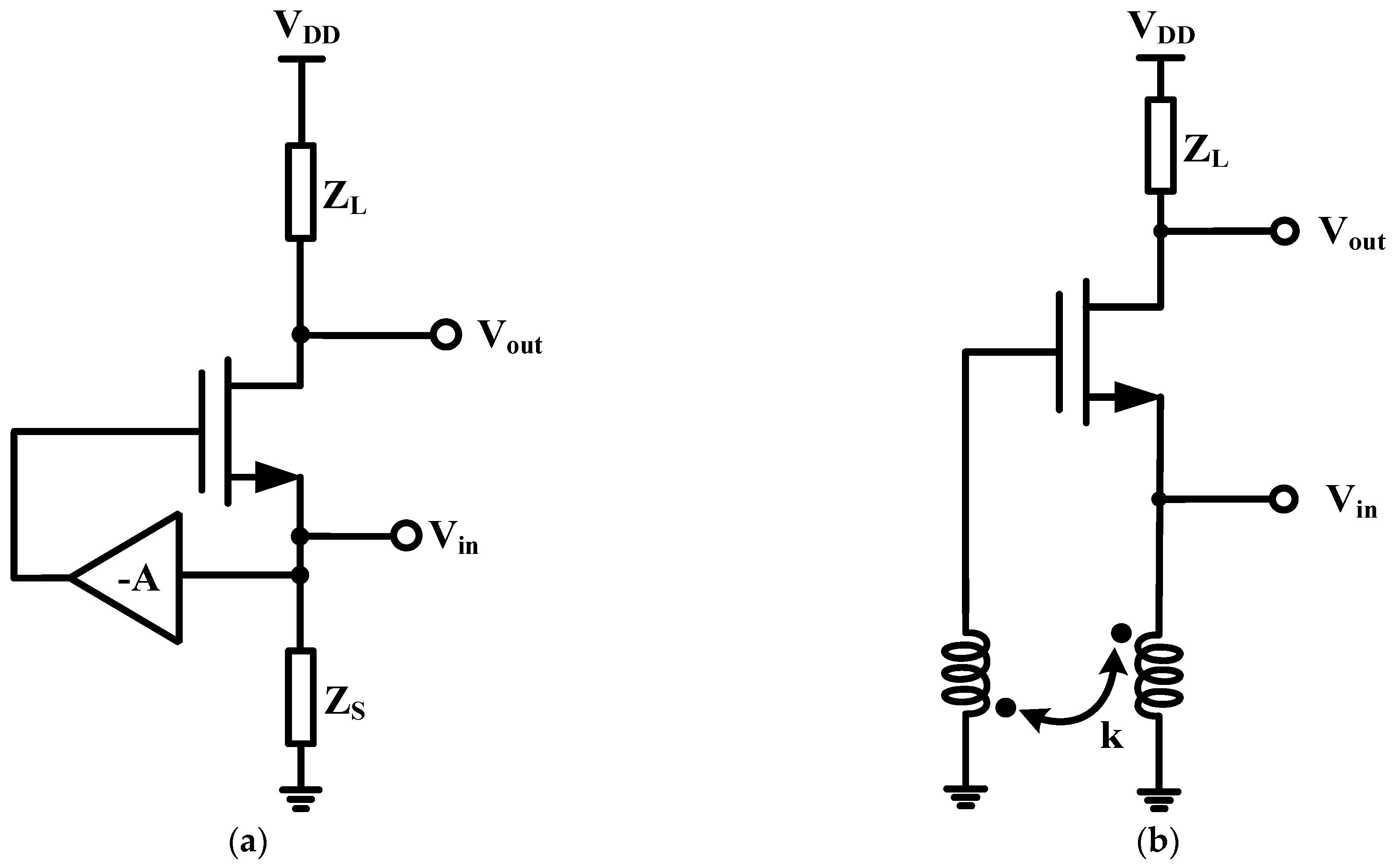
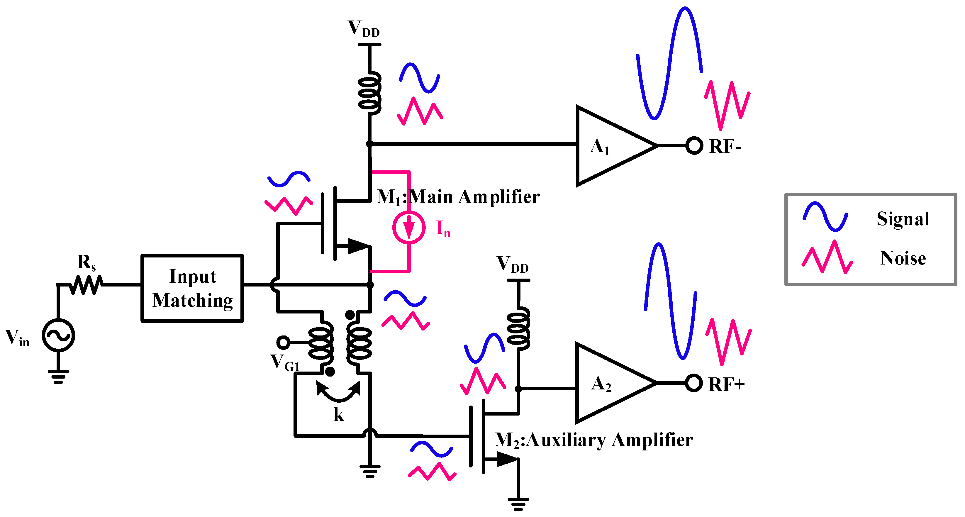
2.1. Transformer-Coupled Gm-Boosted Structure

The basic Gm-boosted structure is shown in Figure 2a, where ZS represents the source impedance at the transistor input and ZL is the load impedance; the noise factor of the common-gate transistor can be expressed as follows:
F = 1 + i n d 2 ¯ 1 1 + g m Z s 2 i n s 2 ¯ g m Z s 1 + g m Z s 2 = 1 + i n d 2 ¯ i n s 2 ¯ 1 g m Z S 2
where ind represents the drain thermal noise current, and ins is the thermal noise generated by the source resistance; these two currents are calculated by the following:
i n d 2 ¯ = 4 k T γ g d s Δ f
i n s 2 ¯ = 4 k T Z s Δ f
the following can be further derived:
F = 1 + 4 k T γ g d s Δ f 4 k T Z S 1 Δ f 1 g m Z S 2     = 1 + γ g d s g m 2 Z S
Under input matching conditions, where ZS = 1/gm and α = gm/gds, this expression becomes the following:
F = 1 + γ α
After introducing the Gm-boosted structure, the effective transconductance becomes (1 + A)gm, and the matching condition is updated to ZS = 1/(1 + A)gm. By substituting these conditions into Equation (4), we obtain Equation (6):
F = 1 + γ α ( 1 + A )
It can be observed that the noise factor decreases. The reason for this improvement is that the effective transconductance has increased, while the minimum noise factor is still determined by process-related parameter α, and the gm in α = gm/gds remains the transistor’s intrinsic transconductance, which is unchanged [15,16].
As shown in Figure 2b, the transformer-coupled structure represents a Gm-boosted implementation in which the signal is fed to the gate via transformer coupling. The transconductance-boosted ratio in this structure is n·k, where n represents the turns ratio between the primary and secondary windings (equivalent to the square root of the inductance ratio), and k represents the transformer coupling coefficient.
In this design, the Gm-boosted structure and noise voltage coupling implemented through a transformer consume significant chip area. To validate the advantage of the Gm-boosted transformer structure, simulations were conducted on both optimized amplifier structures with and without the Gm-boosted transformer. The circuit without the Gm-boosted structure directly applies the input signal to the input of M1 and the gate of M2, resembling the basic common-gate noise-canceling topology. Figure 3 shows the post-optimized gain and noise levels of the two topologies. The maximum gain and minimum noise figure are selected as the simulation parameters, thus excluding the influence of input impedance. It can be observed from Figure 3a that within the ultra-wideband operating range of 26–46 GHz, after the differential combination of the main and auxiliary amplifiers’ output, the maximum gain of topology with the transformer-coupled Gm-boosted structure remains around 10.1–10.5 dB, while the maximum gain of the one without it drops to approximately 5.2–6 dB. Additionally, as shown in Figure 3b, the minimum noise figure of the first-stage amplifier with the Gm-boosted structure is about 2.2–2.4 dB, but upon removing the Gm-boosted transformer, the noise performance deteriorates significantly—minimum noise figure reaches 2.7–3.1 dB. Furthermore, to achieve optimized results, the topology without a Gm-boosted structure implements larger transistor dimensions, resulting in a DC bias current of 51.1 mA and a power consumption of 46 mW. In contrast, the amplifier with the transformer-coupled Gm-boosted structure uses a DC bias current of only 19.7 mA and a power consumption of 17.7 mW. This comparison clearly demonstrates the critical role of the transformer-coupled Gm-boosted structure in optimizing both performance and power consumption in the proposed design circuit.

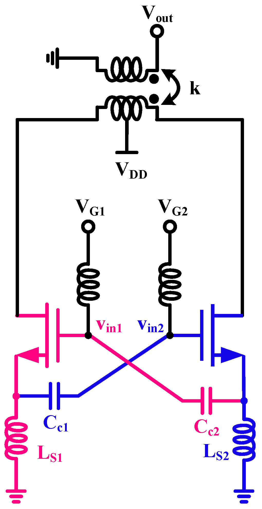
2.2. Asymmetric Cross-Coupling Noise-Canceling Structure

As shown in Figure 4, the second-stage common-source amplifier implements a capacitive cross-coupling structure on the terminals of source degeneration inductors LS1, LS2. At the input, a bias voltage is added to the gate of the common-source amplifier via an inductor, while the small AC signal is generally coupled from the first stage to the inductor connected to the gate. The cross-coupling structure works similarly to a Gm-boosted configuration. The inputs at the gates of the second-stage amplifiers, vin1 and vin2, are out of phase, similar to differential signals. These signals are then capacitively coupled via Cc1 and Cc2 to the source of the other common-source amplifiers, enhancing the Vgs and thereby boosting the equivalent transconductance. After adding a cross-coupling structure to the second stage, the absolute value of the gate-source voltage can be approximately expressed as follows:
| v g s 1 | = | v i n 1 | + C c 1 C g s 1 + C c 1 | v i n 2 | | v g s 2 | = | v i n 2 | + C c 2 C g s 2 + C c 2 | v i n 1 |
In this structure, the two second-stage common-source amplifiers have different transistor dimensions, cross-coupling capacitances, and source degeneration inductances. Moreover, the output signal of the first stage is phase inverted but amplitude unequal. As a result, the entire structure forms an asymmetric cross-coupling topology, which allows for gain and noise optimization according to specific design requirements. Moreover, since cross-coupling is realized through passive capacitive components, little additional noise is introduced.
The effectiveness of the asymmetric cross-coupling can be demonstrated through simulation comparisons. Figure 5 shows the results of gain and noise after matching for the proposed LNA with and without the cross-coupling capacitor Cc1, Cc2. For the topology without cross-coupling, two different optimization strategies were applied, resulting in two different performance outcomes. It can be observed that the LNA with cross-coupling capacitors achieves both flat gain and low noise performance across the ultra-wideband frequency range of 26–46 GHz. In contrast, the LNA without cross-coupling capacitors under Optimization1 achieves a comparable noise figure but suffers from significant degradation in high-frequency gain and an excessively high gain peak at low frequencies. As a result, its 3 dB gain bandwidth fails to cover the target frequency range. On the other hand, the non-cross-coupled LNA under Optimization2 exhibits gain performance similar to that of the proposed LNA but with a severely deteriorated noise figure—its minimum noise increases by approximately 1.2 dB, which is unacceptable for low-noise applications. In fact, the introduction of the cross-coupling structure modifies the relatively fixed parameters in the original second-stage noise-canceling structure. This provides greater design flexibility when facing the trade-off among noise matching, gain matching and conjugate matching in ultra-wideband scenarios, which are generally difficult to balance. The simulation results clearly demonstrate the effectiveness of the proposed asymmetric cross-coupling structure in improving the ultra-wideband performance of the LNA.

3. Circuit Design

3.1. First-Stage Amplifier Design

In the millimeter-wave frequency range, transformer sizes are significantly reduced compared to those at low and mid frequencies. Furthermore, unlike transistor-based active structures, the noise contribution from the transformer is negligible. In addition, the passive nature of the transformer structure results in lower nonlinearity, thereby maintaining the linearity performance of the original LNA design without introducing extra power consumption. The transformer-coupled structure also provides a flexible signal adjusting mechanism and makes it easier to transmit the input signal to the other amplifier. Considering these advantages, the transformer-coupled Gm-boosted structure is adopted in this work.
The complete circuit of the first-stage amplifier is illustrated in Figure 6. The main input amplifier M1 adopts a common-gate topology, while the auxiliary amplifier M2 utilizes a common-source structure. The second-stage amplifier is replaced by A1 and A2 and will be designed after the first-stage amplifier. The single-ended input signal is added to the source of M1, and the original input signal phase at M1’s source is defined as positive. Furthermore, the noise voltage on the primary coil of the transformer in series with M1’s source, which is generated by the channel thermal noise current In, is also defined as having a positive phase. The transformer is coupled according to the dot mark, as shown in the figure, with the coupling coefficient k. A DC bias voltage is applied at the center tap of the secondary coil, which serves as the small-signal ground, and it is mainly determined by the trade-off between gain and power consumption. The non-dot terminal of the secondary coil corresponding to the primary coil is connected to the gate of M1, thereby feeding a negative signal (i.e., an inverted signal) to achieve the Gm-boosted effect. On the other side of the secondary coil, the dot-marked terminal is connected to the gate of the auxiliary amplifier M2, delivering a positive signal in phase with the input signal and a positive noise voltage in phase with M1’s source. In this structure, VG1 provides gate bias for both M1 and M2. The direction of the channel thermal noise current is always from drain to source; thus, the noise voltage across the load inductor at the drain of M1 is negative. In contrast, due to the characteristics of the common-gate amplifier, the signal at M1’s drain remains in phase with the source input, i.e., positive. As for M2, due to the inverting amplification characteristic of the common-source topology, the signal and noise voltages at the drain are once again phase inverted, resulting in a negative output signal and a negative noise voltage. The resulting inverted signal and the in-phase noise voltage can be differentially combined and achieve noise cancellation. In this process, the noise voltage becomes part of the common-mode response, which means it is canceled by the differential architecture.

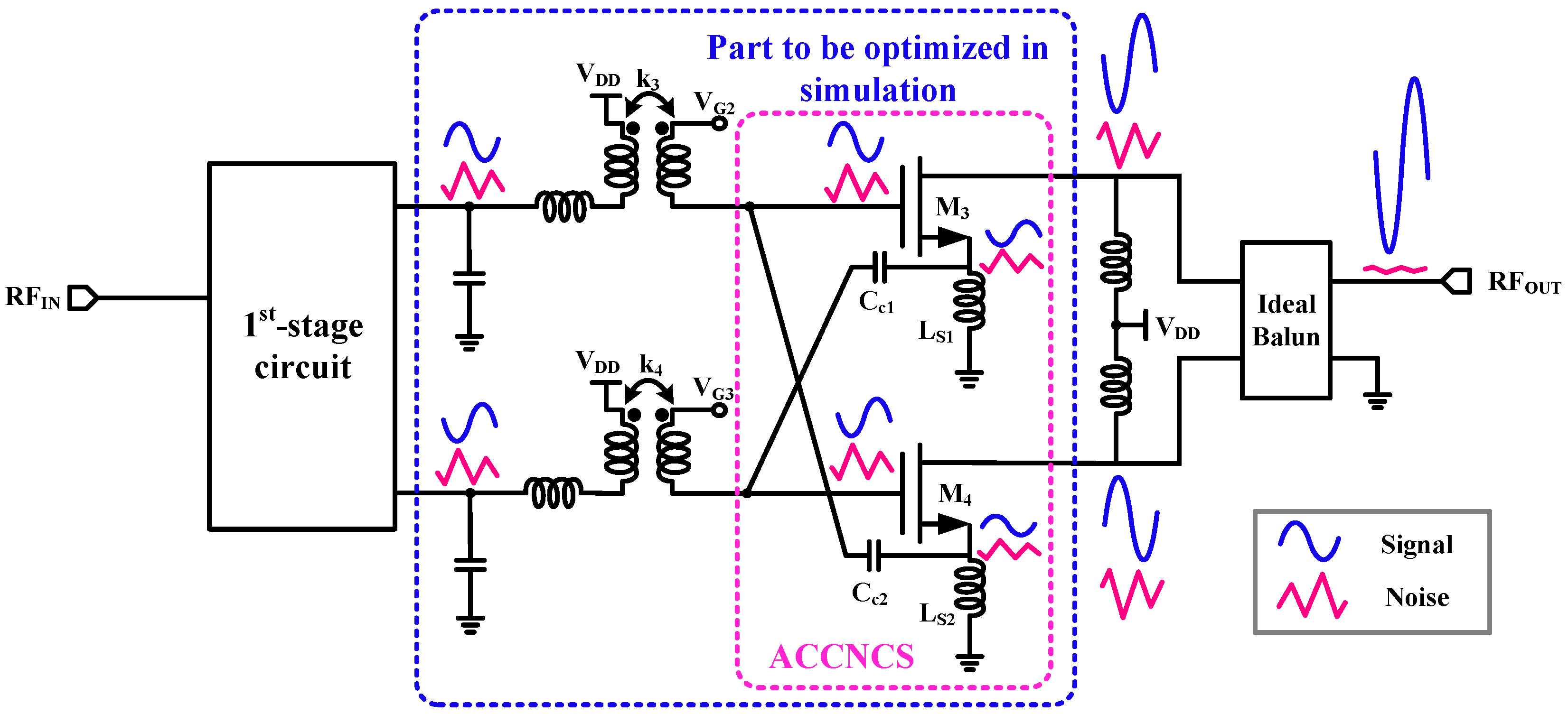
3.2. Second-Stage Amplifier Design

In this LNA design, it is necessary to simultaneously ensure the proper transmission of the output signal from the preceding stage, provide gate biasing, and introduce cross-coupling signals. At the same time, DC bias and AC signals should be added to correct nodes. To satisfy these requirements, a transformer is employed for signal transfer and inter-stage matching. Transformers on both paths are coupled to the dot-marked terminal, so they keep the original relative phase of the signal during transmission. The cross-coupling between the two paths of the second-stage amplifier is implemented as shown in Figure 6, which ensures that the bias voltage is not imposed on the source node of the opposite amplification path. Together with in-phase noise, the AC signal with opposite polarity at the gate of M3 and M4 is cross-coupled to the other transistor’s source, thus adjusting the dimensions and parameters of devices in the second stage. According to the characteristics of inductors blocking DC and capacitors blocking AC, this process does not introduce complex feedforward issues. At the output of M3 and M4, the inverted signal is combined through balun and converted into a single-ended signal, while the in-phase noise is canceled during this process.
Based on the selected amplifier topology and the cross-coupling technique introduced above, the proposed ultra-wideband LNA adopts an asymmetric cross-coupling noise-canceling structure (ACCNCS) for the second-stage design. The first-stage amplifier circuit designed in Section 2.1 is cascaded with the inter-stage matching network. The inter-stage matching network together with the ACCNCS is the part planned to be optimized via simulation in this design step. The schematic used for simulation is shown in Figure 7. In this step, the components mainly being tuned include the transistor dimensions of the second-stage amplifiers; the values of source degeneration inductors LS1, LS2 and the cross-coupling capacitances Cc1, Cc2; and the dimensions of passive components in the inter-stage matching network. Additionally, the selection of bias voltages VG2/VG3 must consider both the effectiveness of noise cancellation and power consumption.
The effect of asymmetric cross-coupling capacitors is quite complex. As demonstrated above, their primary function is adjusting the noise-canceling process in the second stage. This allows the noise-canceling structure to cancel noise effectively while maintaining the gain level and flatness across the ultra-wideband frequency range. The value of the cross-coupling capacitances can be further tuned during the input matching and through multiple iterations, leading to improved overall LNA performance to meet ultra-wideband operation requirements.

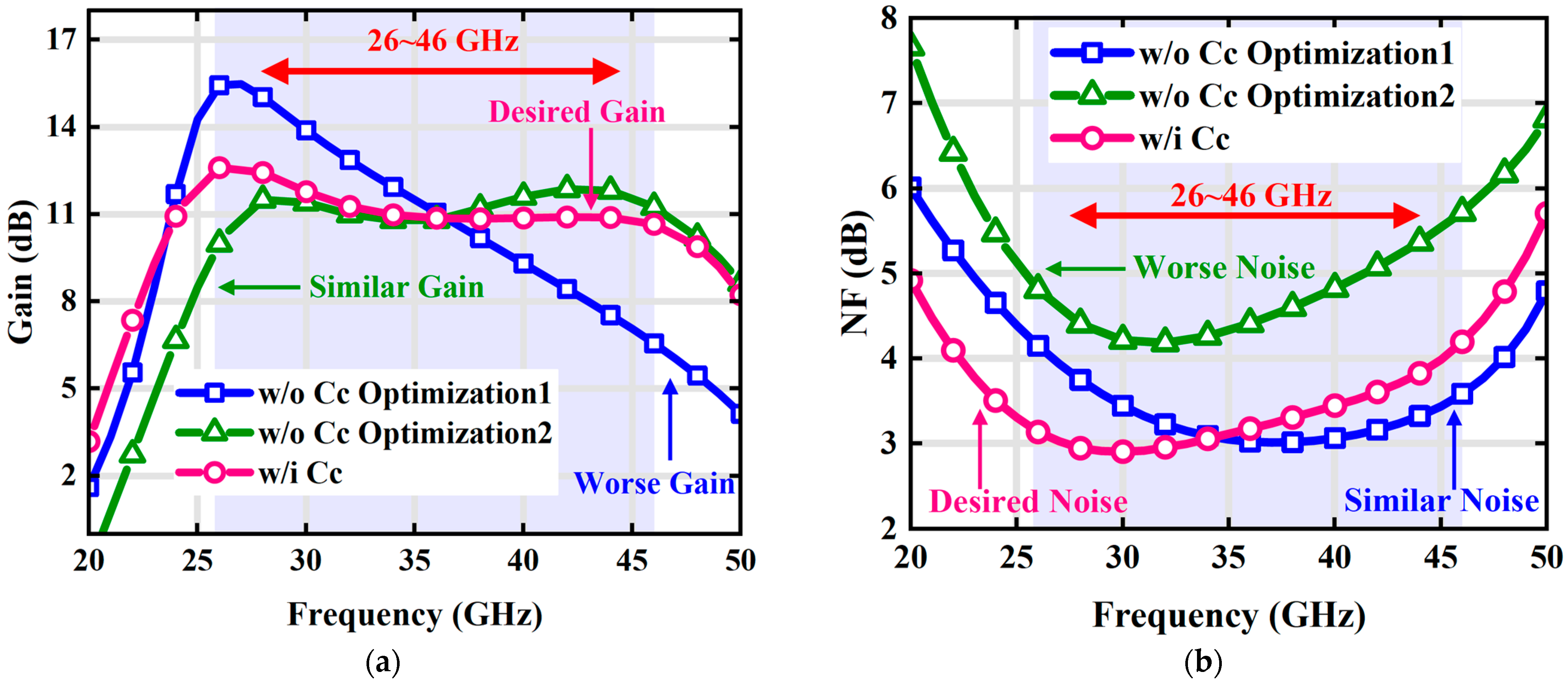
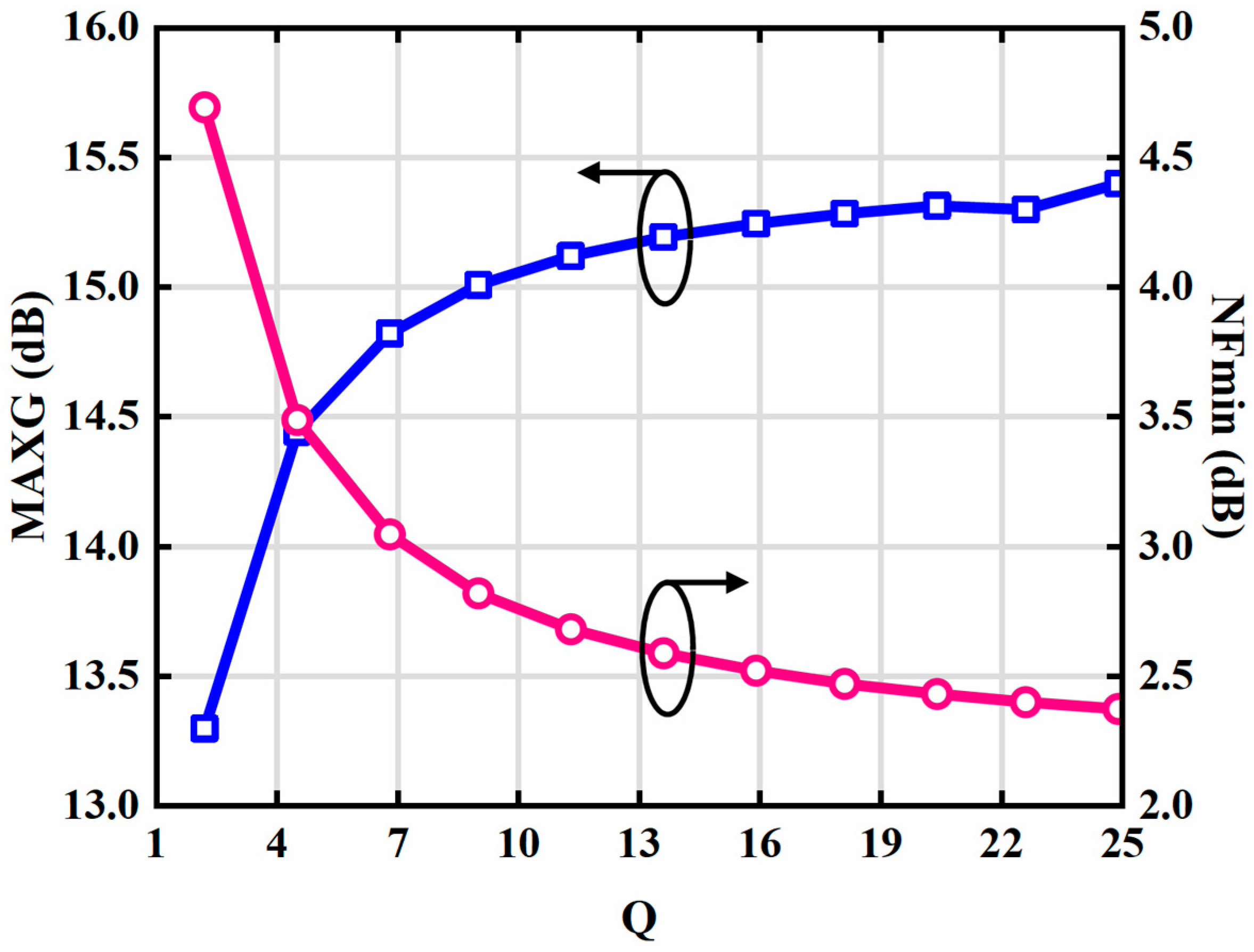
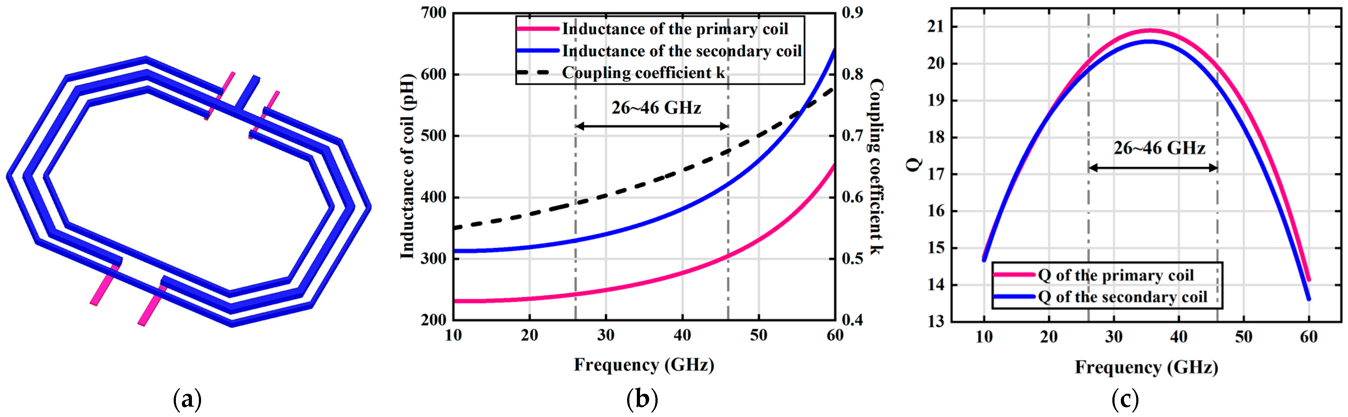
3.3. Transformer Design

Among passive components, the modeling of transformers and inductors is most difficult, as their characteristics are more frequency-dependent than that of capacitors. These components also introduce a series of complex parasitic effects and non-ideal resistive losses. Such non-idealities can have a considerable impact on the overall performance of LNAs. To evaluate these effects, further circuit-level simulations were carried out, focusing on the transformers and inductors employed in the proposed design.
As an example, the transformer between the main amplifier M1 and auxiliary amplifier M2 in the first stage serves not only as a transmission path for the input signal but also as a key structure for realizing the Gm-boosted structure in M1. Therefore, its performance is critical to the function of the whole circuit. Detailed simulations are conducted to examine the influence of the first-stage transformer’s parameters on circuit performance.
In Figure 8, the maximum gain and minimum noise figure at the center frequency of 36 GHz are selected as representative metrics to analyze the influence of the first-stage transformer’s quality factor (Q) for the primary and secondary coil. The results clearly demonstrate that Q significantly affects both gain and noise performance. Higher Q values correspond to increased gain and a reduced noise figure. This is because the quality factor Q represents the magnitude of resistive loss at a given frequency for a specified inductance value, and the Q factor is defined as follows:
Q = 2 π f L R
Resistance in the signal transmission path means thermal noise, which must be minimized in LNA design. This principle applies to most of the transformers and inductors used in the proposed LNA architecture. The difference is only that certain components—such as source degeneration inductors, which are not directly in the main amplification path—exhibit relatively limited influence on gain and noise performance, even when their Q factors are lower.
To ensure that the transformer and inductor meet the design requirements, electromagnetic modeling and simulation were performed. Figure 9a shows the model of the first-stage transformer, which serves both the Gm-boosted structure of the main amplifier M1 and signal transmission to the auxiliary amplifier M2. In this design, the thickest available top metal layer—Metal 9 (M9) (shown in blue in the figure) in the 28 nm process—is utilized as much as possible. With a thickness of 3.5 μm, M9 significantly reduces resistive losses and contributes to achieving high Q performance. Additionally, Metal 8 (M8) (shown in red in the figure) is used to bridge the windings, allowing both the primary and secondary coils to be fully implemented on the low-loss M9 layer. This strategy helps ensure a high Q factor for both coils. In addition, a center tap is drawn from the middle of the secondary coil to provide a DC bias voltage. Figure 9b,c presents the modeling parameters of the transformer. As shown in Figure 9b, the primary coil exhibits an inductance of approximately 280 pH, while the secondary coil has an inductance of about 380 pH. The coupling coefficient falls within the range of 0.6 to 0.7. Figure 9c illustrates that the Q factors of both the primary and secondary coils exceed 20 across the main operating frequency band of 26–46 GHz. Considering the previous analysis of the influence of the coil Q factor on circuit performance, the transformer exhibits characteristics that meet the performance requirements of the first-stage transformer in the proposed LNA. Its combination of moderate coupling and consistently high Q values ensures both effective signal transmission and a minimized noise contribution.

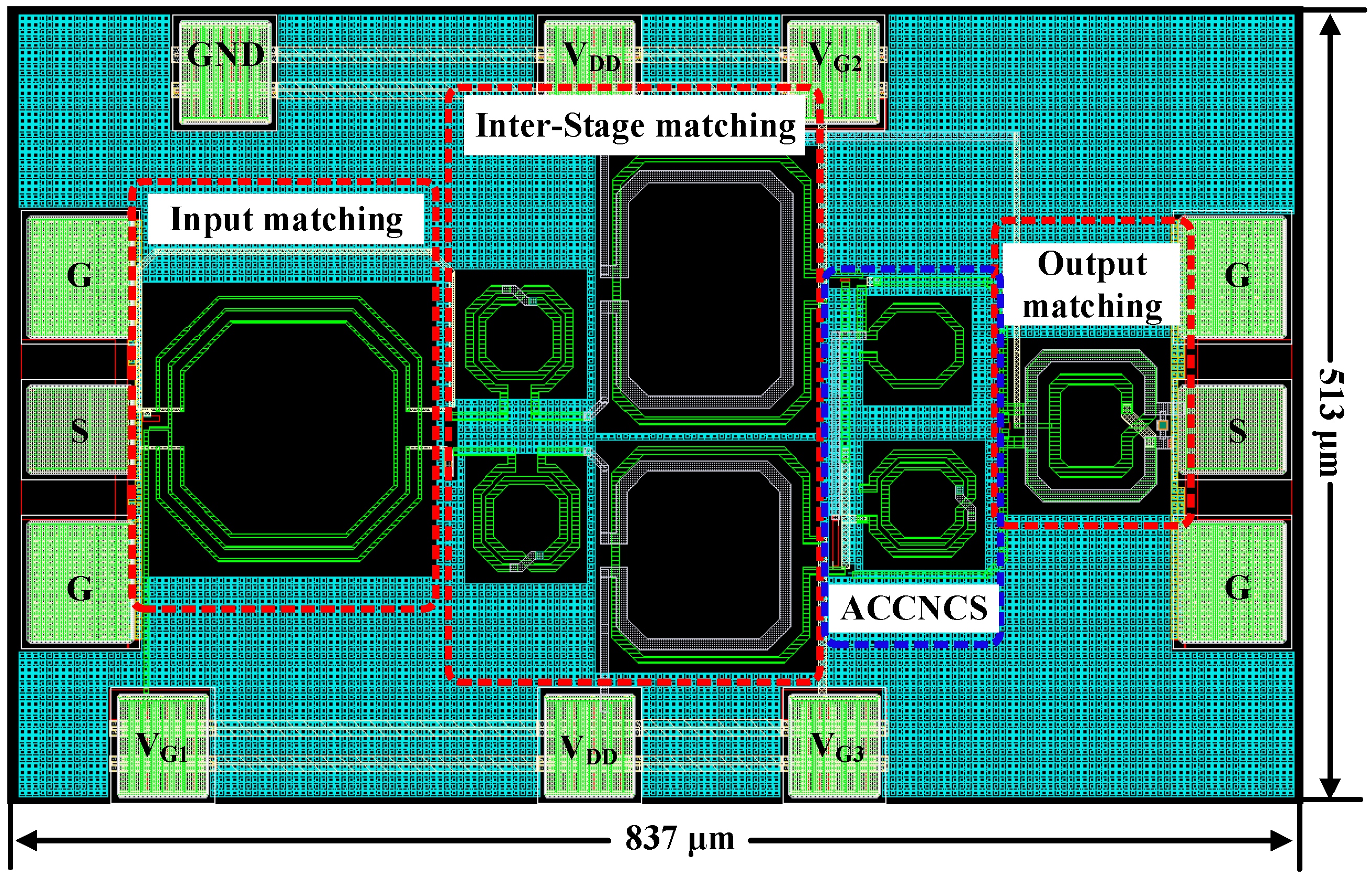
3.4. Complete LNA Circuit with Input and Output Matching Networks

Figure 10 shows the complete circuit diagram of the proposed LNA with two paths. The input matching network is formed by the transformer T1 and parallel capacitors. The first stage consists of two paths, formed by the CG amplifier M1 and the CS amplifier M2. The inter-stage matching network for the two paths is composed of parallel capacitors, series inductors, and two transformers T2, T3. An asymmetric cross-coupling noise-canceling structure (ACCNCS) is achieved by two different CS amplifiers M3, M4 with source degeneration inductors LS1, LS2 and cross-coupling capacitors Cc1, Cc2. Following the ACCNCS, the output matching network is formed by a differential-to-single-ended transformer T4 with two parallel capacitors. Top view of the models of all four transformers T1–T4 implemented in the LNA are shown below the schematic. In this technology, the simulated results show that the transition frequency (fT) of the transistors used in this design is approximately 305 GHz, while the maximum oscillation frequency (fmax) is approximately 230 GHz. This ensures that the transistors can operate stably at high frequencies. Table 1 lists the dimensions and parameters of the main devices corresponding to the schematic of the proposed LNA.

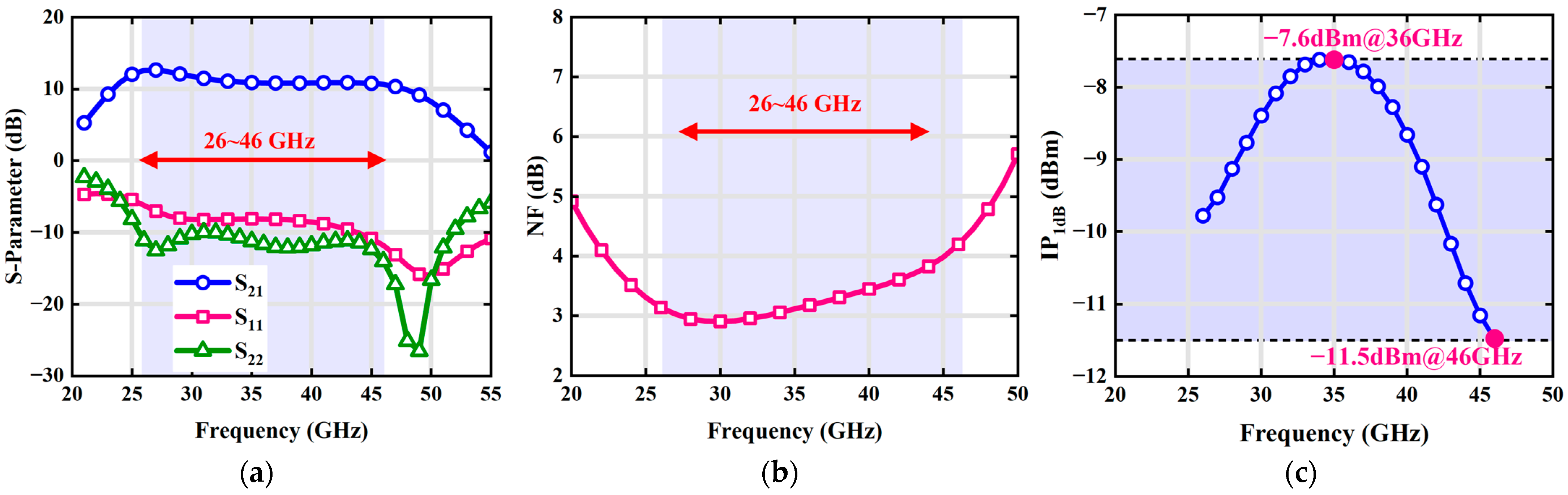
4. Simulation Results

The complete layout of the proposed LNA with GSG and DC pads is shown in Figure 11. And the whole circuit (with PAD) occupies a chip area of 513 × 837 µm2, which is 0.43 mm2, while the core circuit occupies only an area of 335 × 665 µm2, which is 0.23 mm2.
Figure 12a shows the post-simulation results of the S parameters for the proposed LNA. The gain reaches 10.6–12.6 dB over the entire operating frequency band, with S22 less than 10 dB and S11 below −8 dB across 90% of the bandwidth, achieving wideband matching. In addition, Figure 12b shows the noise figure curve of the LNA with ACCNCS, and it can be observed that the LNA maintains a noise figure ranging from 2.9 dB to 4.2 dB across the ultra-wideband frequency range of 26 GHz to 46 GHz. Furthermore, as shown in Figure 12c, the LNA exhibits an IP1dB greater than −11.5 dBm across the operating band, reaching −7.6 dBm near the center frequency.
Table 2 summarizes the performance of the proposed LNA and compares it with state-of-the-art publications. Compared with other LNAs, this work achieves good gain, noise, and linearity performance over a wide operating frequency band, with a competitive fractional bandwidth (FBW) of 56%. In order to evaluate and compare the overall performance of LNAs, a widely recognized figure of merit (FoM) is employed, defined as follows [17]:
FoM = Gain MAX [ dB ] × BW [ GHz ] ( NF min [ dB ] 1 ) × P DC [ mW ]

5. Conclusions

This paper presents an ultra-wideband LNA with a new cross-coupling noise-canceling technique designed using a 28 nm CMOS process. The first stage employs the CG Gm-boosted technique, while the second stage (ACCNCS) utilizes capacitive cross-coupling to improve wideband gain matching and noise matching. Input, output, and inter-stage matching are achieved through transformer, inductor, and capacitor networks. The LNA occupies a core layout area of 0.23 mm2 and operates across a frequency range of 26 to 46 GHz, for which the FBW is 56%. Post-layout simulation results demonstrate a peak gain of 12.6 dB and a noise figure ranging from 2.9 to 4.2 dB over the entire operation band. Under a 0.9 V supply, the input 1 dB compression point (IP1 dB) is −11.5 to −7.6 dBm, with a total power consumption of 22 mW.

Author Contributions

Conceptualization, investigation, design, and writing, Y.C.; review and editing, Y.C., K.H. and K.M.; supervision, K.M.; funding acquisition, K.M. All authors have read and agreed to the published version of the manuscript.

Funding

This work was supported in part by the National Natural Science Foundation of China under Grant 62341409, and in part by Guangdong S&T Program under grant 2024B0101020001.

Data Availability Statement

Data are contained within the article.

Conflicts of Interest

The authors declare no conflicts of interest.

References

  1. Shaeffer, D.K. A 1.5-V, 1.5-GHz CMOS Low Noise Amplifier. IEEE J. Solid-State Circuits 1997, 32, 745–759. [Google Scholar] [CrossRef]
  2. Lu, Y.; Yeo, K.S.; Cabuk, A. A Novel CMOS Low-Noise Amplifier Design for 3.1 to 10.6-GHz Ultra-Wide-Band Wireless Receivers. IEEE Trans. Circuits Syst. 2006, 53, 1683–1692. [Google Scholar]
  3. Zhang, J.; Zhao, D.; You, X. A 20-GHz 1.9-mW LNA using gm-boost and current-reuse techniques in 65-nm CMOS for satellite communications. IEEE J. Solid-State Circuits 2020, 55, 2714–2723. [Google Scholar] [CrossRef]
  4. Lu, W.; Zhao, C.; Yu, Y.; Jiang, Z.; Wu, Y.; Liu, H.; Kang, K. A Ku-band CMOS LNA with transformer feedforward gm-boosting technique. In Proceedings of the IEEE MTT-S International Microwave Workshop Series on Advanced Materials and Processes for RF and THz Applications (IMWS-AMP), Chengdu, China, 20–22 July 2016. [Google Scholar]
  5. Bozorg, A.; Staszewski, R.B. A 0.02–4.5-GHz LN(T)A in 28-nm CMOS for 5G Exploiting Noise Reduction and Current Reuse. IEEE J. Solid-State Circuits 2021, 56, 404–415. [Google Scholar] [CrossRef]
  6. Kim, D.; Jang, S.; Lee, J.; Im, D. A Broadband PVT-Insensitive All-nMOS Noise-Canceling Balun-LNA for Subgigahertz Wireless Communication Applications. IEEE Microw. Wirel. Compon. Lett. 2021, 31, 165–168. [Google Scholar] [CrossRef]
  7. Joo, S.; Choi, T.Y.; Jung, B. A 2.4-GHz Resistive Feedback LNA in 0.13-um CMOS. IEEE J. Solid-State Circuits 2009, 44, 3019–3029. [Google Scholar] [CrossRef]
  8. Bruccoleri, F.; Klumperink, E.; Nauta, B. Noise cancelling in wide-band CMOS LNAs. IEEE Int. Solid-State Circuits 2002, 1, 406–407. [Google Scholar]
  9. Blaakmeer, S.C.; Klumperink, E.A.M.; Leenaerts, D.M.W.; Nauta, B. Wideband balun-LNA with simultaneous output balancing, noise-canceling and distortion-canceling. IEEE J. Solid-State Circuits 2008, 43, 1341–1350. [Google Scholar] [CrossRef]
  10. Wang, H.; Zhang, L.; Yu, Z. A Wideband Inductorless LNA with Local Feedback and Noise Cancelling for Low-Power Low-Voltage Applications. IEEE Trans. Circuits Syst. I Regul. Pap. 2010, 57, 1993–2005. [Google Scholar] [CrossRef]
  11. Tiwari, S.; Mukherjee, J. An Inductorless Noise Cancelling Wideband Balun LNA with Dual Shunt Feedback and Current Reuse. In Proceedings of the 2019 IEEE 62nd International Midwest Symposium on Circuits and Systems (MWSCAS), Dallas, TX, USA, 4–7 August 2019; pp. 432–435. [Google Scholar]
  12. Kong, S.; Lee, H.D.; Jang, S.; Park, J.; Kim, K.S.; Lee, K.C. A 28-GHz CMOS LNA with stability-enhanced Gm-boosting technique using transformers. In Proceedings of the 2019 IEEE Radio Frequency Integrated Circuits Symposium (RFIC), Boston, MA, USA, 4–6 June 2019. [Google Scholar]
  13. Elkholy, M.; Shakib, S.; Dunworth, J.; Aparin, V.; Entesari, K. A Wideband Variable Gain LNA With High OIP3 for 5G Using 40-nm Bulk CMOS. IEEE Microw. Wirel. Compon. Lett. 2018, 28, 64–66. [Google Scholar] [CrossRef]
  14. Chauhan, V.; Floyd, B. A 24–44 GHz UWB LNA for 5G cellular frequency bands. In Proceedings of the 11th Global Symposium on Millimeter Waves (GSMM), Boulder, CO, USA, 22–24 May 2018. [Google Scholar]
  15. Razavi, B. Design of Analog CMOS Integrate Circuits, 2nd ed.; McGraw-Hill Education: New York, NY, USA, 2015; pp. 198–244. [Google Scholar]
  16. Li, X.; Shekhar, S.; Allstot, D.J. Gm-boosted common-gate LNA and differential colpitts VCO/QVCO in 0.18-μm CMOS. IEEE J. Solid-State Circuits 2005, 40, 2609–2619. [Google Scholar]
  17. Huang, B.J.; Lin, K.Y.; Wang, H. Millimeter-wave low power and miniature CMOS multicascode low-noise amplifiers with noise reduction topology. IEEE Trans. Microw. Theory Tech. 2009, 57, 3049–3059. [Google Scholar] [CrossRef]
  18. Jamil, S.; Usman, M.; Atiq, H.; Ramzan, R. 28–32 GHz Wideband LNA for 5G Applications. In Proceedings of the 1st International Conference on Microwave, Antennas & Circuits (ICMAC), Islamabad, Pakistan, 21–22 December 2021. [Google Scholar]
  19. El-Nozahi, M.; Sánchez-Sinencio, E.; Entesari, K. A millimeter-wave (23–32 GHz) wideband BiCMOS low-noise amplifier. IEEE J. Solid-State Circuits 2010, 45, 289–299. [Google Scholar] [CrossRef]
  20. Kobal, E.; Siriburanon, T.; Chen, X.; Nguyen, H.M.; Staszewski, R.B.; Zhu, A. A Gm-Boosting Technique for Millimeter-Wave Low-Noise Amplifiers in 28-nm Triple-Well Bulk CMOS Using Floating Resistor in Body Biasing. IEEE Trans. Circuits Syst. I Regul. Pap. 2022, 69, 5007–5017. [Google Scholar] [CrossRef]
  21. Fang, C.; Wu, Q.; Wang, H.; Hong, W. A 24-40 GHz Wideband LNA with Gain Compensation in 40-nm CMOS for 5G Applications. In Proceedings of the 16th UK-Europe-China Workshop on Millimetre Waves and Terahertz Technologies (UCMMT), Guangzhou, China, 31 August–3 September 2023. [Google Scholar]
  22. Zhong, Y.; Du, J.; Li, Y. A 24-27GHz High Linearity LNA in 40nm CMOS Technology. In Proceedings of the 2024 IEEE International Symposium on Radio-Frequency Integration Technology (RFIT), Chengdu, China, 28–30 August 2024. [Google Scholar]
Figure 1. Configuration of the proposed LNA.
Electronics 14 01904 g001
Figure 2. Gm-boosted structure and its implementation: (a) schematic of the common-gate amplifier with a Gm-boosted structure; (b) common-gate amplifier with a transformer-coupled Gm-boosted structure.
Electronics 14 01904 g002
Figure 3. Post-optimization maximum gain and minimum noise figures of two topologies: (a) maximum gain with and without a transformer-coupled Gm-boosted structure; (b) minimum noise figure with and without a transformer-coupled Gm-boosted structure.
Electronics 14 01904 g003
Figure 4. Cross-coupling structure implemented on a common-source amplifier with a source degeneration inductor.
Electronics 14 01904 g004
Figure 5. Performance comparison of LNAs with and without a cross-coupled structure: (a) maximum gain comparison; (b) minimum noise figure comparison.
Electronics 14 01904 g005
Figure 6. Construction of the first stage of the proposed LNA.
Electronics 14 01904 g006
Figure 7. Schematic used for the optimization of the second-stage amplifiers and inter-stage matching network.
Electronics 14 01904 g007
Figure 8. Simulated influence of the first-stage transformer coil quality factor (Q) on the LNA’s maximum gain and minimum noise figure.
Electronics 14 01904 g008
Figure 9. Model and key parameters of the first-stage transformer: (a) transformer model; (b) inductance of the primary coil, secondary coil, and coupling coefficient k; (c) Q factor of the primary coil and the secondary coil.
Electronics 14 01904 g009
Figure 10. Schematic of the proposed LNA with a new cross-coupling noise-canceling technique.
Electronics 14 01904 g010
Figure 11. Layout of the proposed LNA.
Electronics 14 01904 g011
Figure 12. Post-simulation results of the proposed LNA: (a) S parameters; (b) noise figure; (c) input 1 dB compression point.
Electronics 14 01904 g012
Table 1. Main device dimensions and parameters.
DeviceD/PDeviceD/PDeviceD/PDeviceD/P
M1(1.5 μm/30 nm) × 16L1270 pHL7320 pHk10.7
M2(1 μm/30 nm) × 16L2400 pHL8200 pHk20.7
M3(2 μm/30 nm) × 32L3300 pHL9300 pHk30.6
M4(1 μm/30 nm) × 16L4400 pHL10300 pHk40.6
Cc110 fFL5300 pHLs180 pHVG10.55 V
Cc2500 fFL6250 pHLs2350 pHVG2/VG30.5 V
Table 2. Performance summary and comparison with state-of-the-art alternatives.
ReferenceThis Work S[12] M[13] M[18] S[19] M[20] M[21] S[22] S
Tech28 nm CMOS65 nm CMOS40 nm CMOS65 nm CMOS180 nm BiCMOS28 nm CMOS40 nm CMOS40 nm CMOS
Frequency (GHz)26–4624.9–32.526–3326–33.423–3224.7–29.524–4024–27
GainMAX (dB)12.618.32718.51219.12013.6
NF (dB)2.9–4.23.25–4.23.3–4.334.5–6.33.3–3.53.75.8
IP1dB (dBm)−11.5 to −7.6−24−21.6−24.5−16.3 to −14.5−8.7−15.9−4.2
PDC (mW)2220.531.4171325.547.250.8
Core Area (mm2)0.230.110.260.080.250.170.220.34
FBW *56%26%24%25%42%18%50%12%
FoM6.033.022.624.032.371.562.510.14
S: simulated result; M: measured result; *: fractional bandwidth, FBW = 2 (fH − fL)/(fH + fL).
Disclaimer/Publisher’s Note: The statements, opinions and data contained in all publications are solely those of the individual author(s) and contributor(s) and not of MDPI and/or the editor(s). MDPI and/or the editor(s) disclaim responsibility for any injury to people or property resulting from any ideas, methods, instructions or products referred to in the content.

