Abstract
We report gallium nitride (GaN) vertical trench junction barrier Schottky (TJBS) diodes and systematically analyzed the effects of the key design parameters on the reverse and forward characteristics of the devices. By taking advantage of the shielding effects from both the trenches and pn junctions in the TJBS structure, the high electric field at the Schottky contact region can be effectively suppressed. We found that the doping concentration, thickness, and spacing of p-GaN, as well as the depth and angle of the trench sidewalls are closely associated with the electric field distribution and the reverse characteristics of the TJBS diodes. With an optimal set of design parameters, the local electric field crowding at either the corner of the trench or the edge of the p-GaN can also be alleviated, resulting in a boosted breakdown voltage of up to 1250 V in the TJBS diodes. In addition, an analytical model was developed to explore the physical mechanism behind the forward conduction behaviors. We believe that the results can provide a systematical design strategy for the development of low-loss, high-voltage, and high-power GaN power diodes towards an efficient power system.
1. Introduction
Gallium nitride (GaN) is widely used in high-voltage and high-power devices due to its advantages of wide bandgap, high electron mobility and high critical electric field as compared to silicon (Si) and silicon carbide (SiC) [1,2]. Recently, GaN-based vertical power devices have shown a great potential for the next generation of high-efficiency power systems [3,4,5]. Due to their unique properties of a fast switching speed, low turn-on voltage and high-current capability, GaN vertical Schottky barrier diodes (SBDs) have attracted tremendous attention and are considered as promising and indispensable components in modern power systems [6,7,8]. However, conventional vertical GaN SBDs typically suffer from the Schottky barrier lowering effect induced by the high electric field at the Schottky junction interface, which results in a large leakage current and premature breakdown of the devices [9].
Several approaches have been proposed to modulate the electric field at the Schottky contact region to alleviate the reverse leakage and improve the breakdown of the devices. Trench metal–insulator–semiconductor (MIS) barrier Schottky (TMBS) structures have been proven to be effective by utilizing a MIS structure to shield the electric field at the Schottky surface [10,11,12]. An alternative way to improve the reverse characteristics of the GaN vertical SBDs is to employ a pn junction in the vicinity of the Schottky interface, such as merged pn-Schottky (MPS) [13,14], and junction barrier Schottky (JBS) structures [15,16,17], which differ in that the p-type region of MPS diodes forms an ohmic contact with the anode metal, and the anode of JBS diodes forms a Schottky contact with the p-GaN region. Compared to TMBS structures, the fabrication of MPS and JBS structures does not involve the deposition of an insulating dielectric layer, which is accompanied by a high density of interface and bulk traps, sequentially degrading the dynamic performance of the devices. However, the ion implantation and activation technology for p-type GaN is far from mature, resulting in a low concentration and mobility of the activated free holes within the material [18,19]. Therefore, the performance of the MPS diodes is greatly limited due to the difficulty in forming ohmic contact to the implanted p-type region. On the other hand, the anode of the JBS diodes forms Schottky contact with the p-GaN region, which simplifies the fabrication process.
GaN-based junction barrier Schottky (JBS) diodes have been extensively studied. Koehler et al. and Zhang et al. experimentally demonstrated enhanced breakdown voltage in JBS diodes compared to that of conventional SBDs [15,16]. Zhou et al. demonstrated excellent dynamic performance from GaN JBS diodes by ion implantation [7,17], which showed great potential of GaN vertical JBS diodes for high-voltage and high-power applications. However, the enhancement of the reverse characteristics by the JBS structure rely heavily on the adjacent pn junctions to alleviate the electric field crowding at the Schottky interface [20,21,22]. Typically, a deep pn junction into the drift layer is desired for the purpose of effective electric field shielding. A relatively high implantation energy is demanded to form a deep p-type region [19,23], which may induce high defect density either at the interface or within the bulk p-GaN [24]. Therefore, the depth of the pn junction in the currently reported GaN JBS diodes is typically limited to 0.8 μm [7,15,16,17], which largely limits the performance of the JBS diodes.
In this paper, we propose for the first time a trench JBS (TJBS) structure with p-GaN surrounded mesa edges, which takes advantages of both the trench structures and pn junctions simultaneously. The presence of the trenches helps to achieve a deeper pn junction in the drift layer for a more effective electric field shielding effect while at the same time avoiding the utilization of high-energy ion implantation, and thus reducing the density of defects. Furthermore, the influence of the key parameters on the reverse and forward characteristics of GaN-based TJBS diodes are investigated and analyzed systematically by simulation. The results can provide a theoretical guideline for the development of high performance GaN-based TJBS diodes for potential applications including fast charging, automobiles, and energy harvesting.
2. Device Architectures and Principles
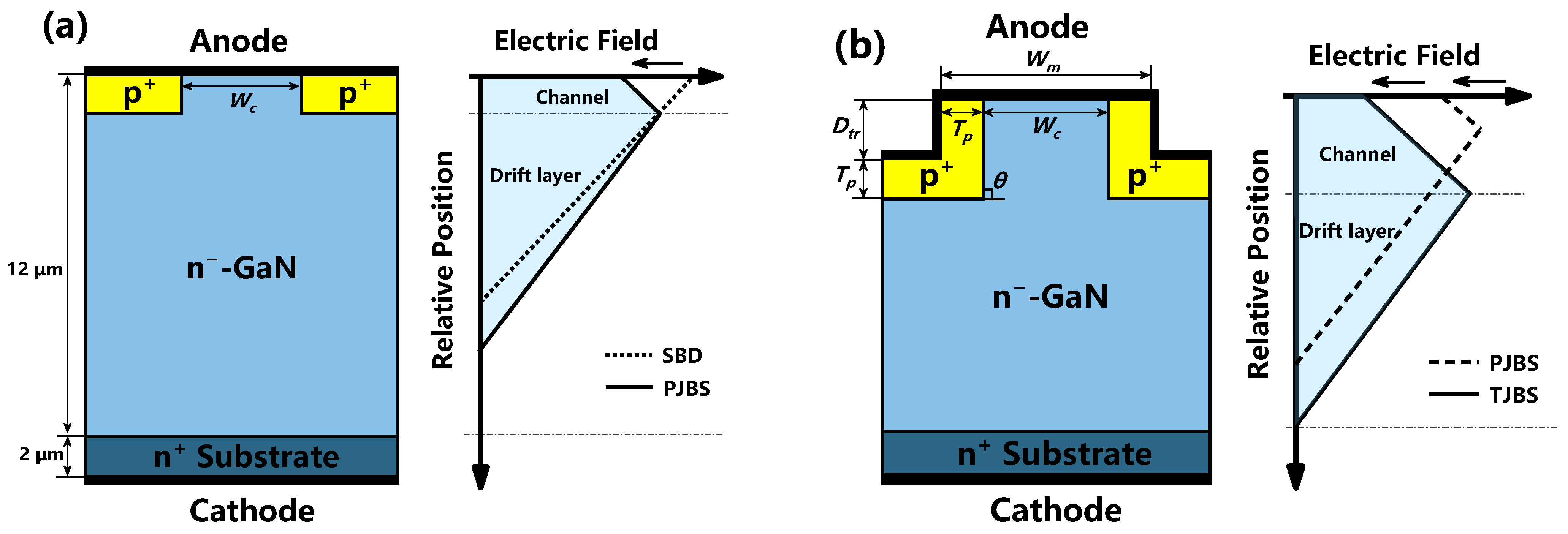
Figure 1a,b show the schematic diagram of the conventional planar JBS (PJBS) diodes and the TJBS diodes. Both devices consist of a 2-μm-thick n+-GaN substrate (Si = 5 × 1018 cm−3) and a 12-μm-thick n−-GaN drift layer, except that the pn junction in the TJBS diodes is deeper than that in the PJBS diode due to the existence of the trench. The anode on the top of the device is set as a Schottky contact, and the cathode on the back of the GaN substrate is an ohmic contact. For an explicit understanding of the electric field shielding effect by the TJBS structure, we plot and compare the schematic one-dimensional (1-D) electric field distributions along the midline of the GaN-based PJBS and GaN-based TJBS, as shown in Figure 1. While the conventional SBD suffers from a high electric field at the Schottky interface [shown by the triangular electric field distribution in Figure 1a], the PJBS and TJBS structures can effectively alleviate the electric field crowding effect and result in a quadrilateral electric field distribution into the drift layer. Thanks to the combined effect by the trench and p-GaN structures, a stronger electric field shielding effect can be observed from the TJBS structure in Figure 1b, which allows a substantial reduction of the electric field at the Schottky surface, compared to the PJBS structure. Meanwhile, the electric field peak moves further into the drift layer due to the adoption of the trench and allows the formation of deeper pn junction.
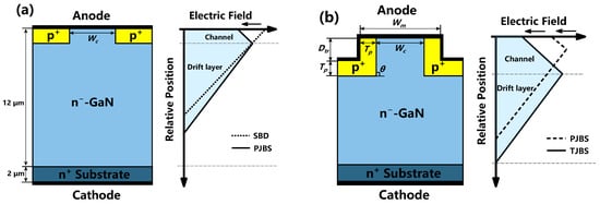
Figure 1.
Cross-sectional schematic diagram and electric field distribution along the channel midline of: (a) the conventional PJBS diodes; and (b) the TJBS diodes.
The reverse blocking capability of TJBS diodes is dominated by the electric field distribution, which is closely correlated with the electric field shielding effect from the pn junction and the vertical trench structure. Therefore, the influence of the key design parameters on the device performance is investigated by varying the doping concentration and the thickness of the p-GaN (Tp), the width of the channel (Wc) between adjacent p-GaN, the depth of the trench (Dtr), and the angle (θ) of the trench slope.
We conduct the numerical investigation based on the Advanced Physical Models of Semiconductor Devices (APSYS) software [25]. The key physical models used in the simulation include models for carrier drift–diffusion, generation–recombination, continuity and Poisson equations, low-field mobility, saturation velocity, and impact ionization. The breakdown process of the device is mainly determined by the impact ionization model, in which the impact ionization coefficients of electrons and holes of GaN are set according to literature [12,26,27], and the impact ionization coefficients of electrons and holes, as a function of the electric field (E) in the drift layer, can be expressed as
On the other hand, the incomplete ionization model can accurately reflect the incomplete ionization of Mg acceptor within GaN under equilibrium condition, which accounts for the acceptor ionization energy of 200 meV above the valence band maximum. The concentration of ionized acceptors can be calculated by the following expression.
where is the acceptor degeneracy factor, and EF is the Fermi level, EA is the acceptor level. Furthermore, the concentration of ionized Mg acceptors is considered to be much higher in the simulation procedure under non-equilibrium conditions than under equilibrium conditions, as experimentally reported in Reference [28]. To ensure that the models and parameters used in this work represent an actual device accurately, the simulated I-V characteristics of a standard SBD were fitted and calibrated with the experimental results [29]. Figure 2 shows a good agreement between the forward and reverse curves of the simulated and the measured results, which demonstrates the effectiveness of the model and parameters used in this work. The breakdown voltage (BV) is defined as the reverse bias value corresponding to a current density of 1 A/cm2.
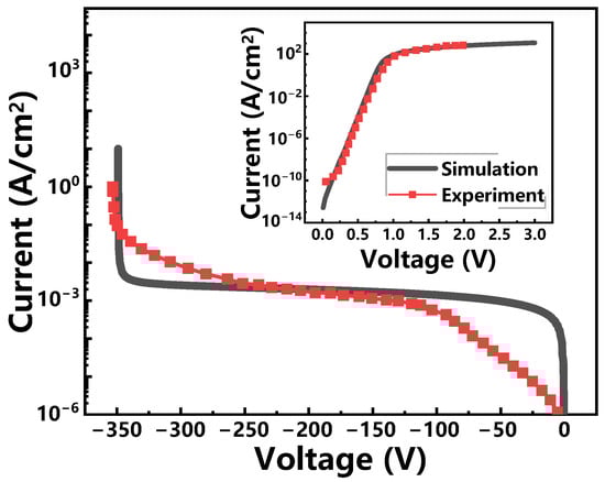
Figure 2.
Forward bias (inset) and reverse breakdown comparison of the simulated and experimental data. Adapted from [29].
3. Results and Discussion
3.1. Effect of p-Doping Concentration and Thickness on the Reverse Blocking Performances of TJBS Diodes
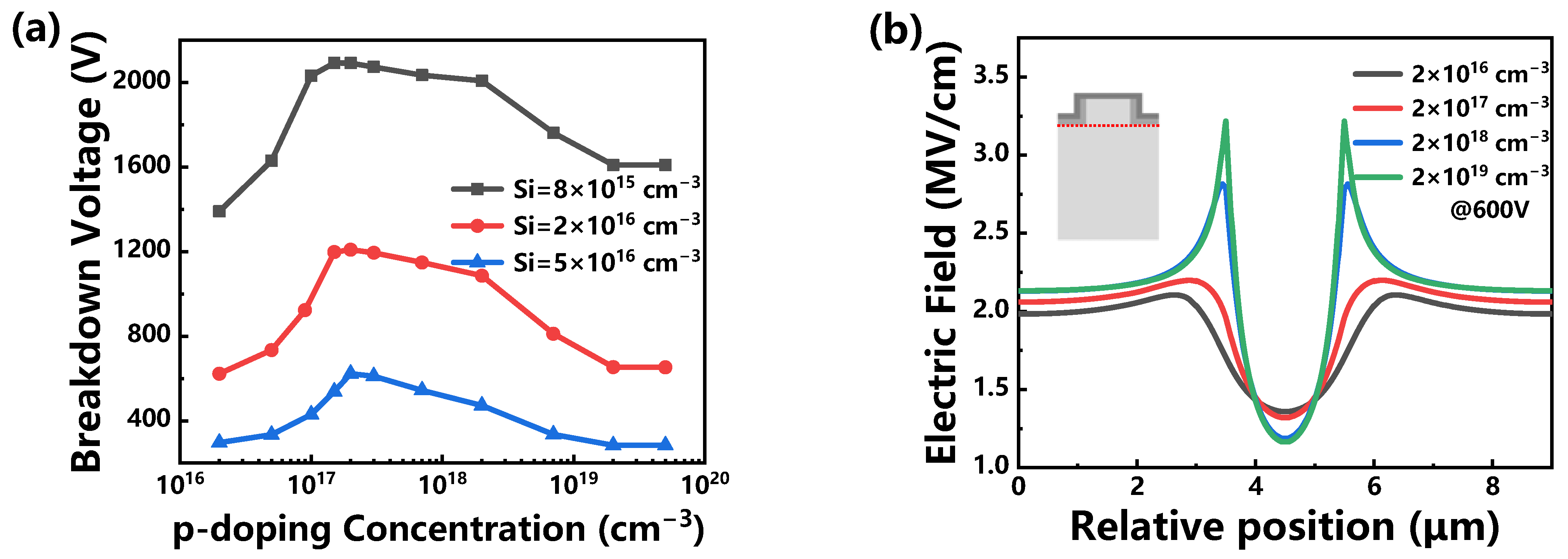
Figure 3a depicts the influence of p-doping concentration (acceptor concentration) on the BV of the TJBS diode for different drift layer doping concentrations. Other key parameters Wc, Dtr and Tp of the TJBS diode are kept at constant values of 2 μm, 1 μm and 0.5 μm respectively. For a given p-doping concentration, the breakdown voltage increases with decreased drift layer doping concentration, owing to the increased depletion depth in the drift region at reverse bias condition. On the other hand, a similar variation trend of the breakdown voltage with the p-doping concentration can be observed with different drift layer doping concentrations. As the p-doping concentration increases, the breakdown voltage of the TJBS diodes first increases and then decreases. A peak breakdown value of 1210 V is recorded with a p-doping concentration of 2 × 1017 cm−3 and a drift layer doping concentration of 2 × 1016 cm−3. Note that the p-doping concentration for the optimum breakdown characteristics is slightly different for TJBS diodes with different drift layer doping concentrations. A lower p-doping concentration is required to achieve the best breakdown voltage for the TJBS diodes with a lower drift doping concentration.
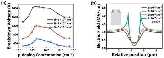
Figure 3.
(a) Breakdown voltage as a function of p-doping concentration for TJBS diodes with different drift layer concentrations; and (b) electric field profiles along the bottom of p-GaN for TJBS diodes with different p-doping concentrations at the reverse bias of 600 V when the drift layer concentration is 2 × 1016 cm−3.
To explore the breakdown mechanism of the TJBS diodes with different p-doping concentrations, we extracted the lateral 1-D electric field profiles from the bottom interface between p-GaN and the n−-GaN drift layer, as shown by the dash line in the inset of the Figure 3b. With a high p-doping concentration of 2 × 1018 cm−3 and above, a high electric field can be observed at the corner of the p-GaN structure, which exceeds the critical breakdown field of GaN and leads to premature breakdown. A more uniform distribution of the electric field can be observed with p-doping concentration of 2 × 1017 cm−3, which can result in an improved breakdown voltage compared to that at a higher p-doping concentration. With a p-doping concentration of 2 × 1016 cm−3, a further reduction in the electric field value is recorded at the bottom of the p-GaN. However, the corresponding breakdown voltage of the TJBS diodes is lower, which cannot be explained with the 1-D electric field profile in Figure 3b.
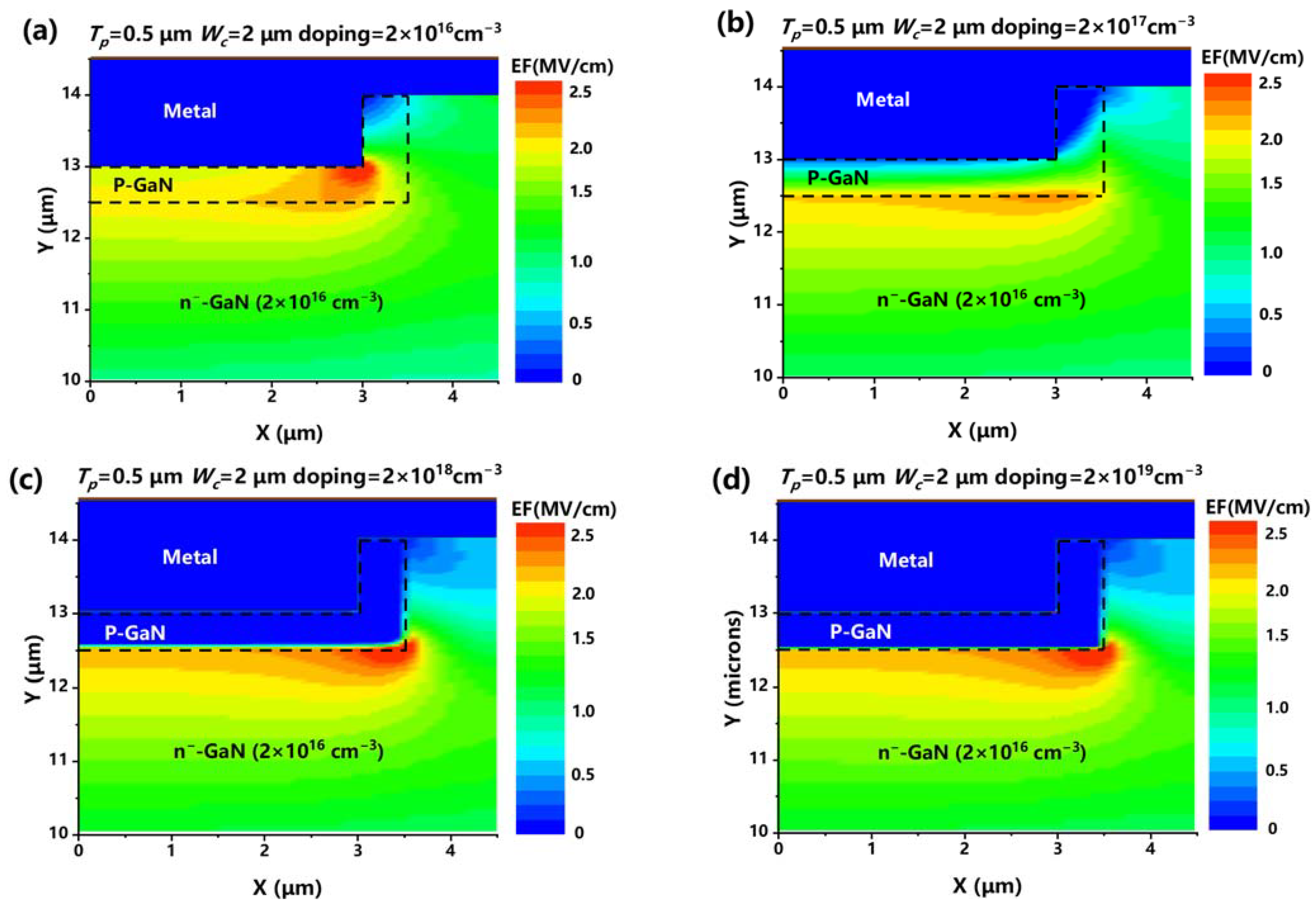
For the purpose of understanding the electric field distribution more explicitly, we compare the two-dimensional (2-D) electric field contours of the TJBS diodes with different p-doping concentrations in Figure 4. With a p-doping concentration of 2 × 1016 cm−3 in Figure 4a, the majority of the electric field concentrates at the corner of the trench, leading to a premature breakdown of the TJBS diodes. Due to the insufficient charge coupling effect by the pn junction, only a negligible proportion of the electric field is moved from the trench corner to the bottom of the p-GaN, which corresponds to the lowest value of the electric field in the 1-D electric field profile from Figure 3b and well explains the reduced breakdown voltage with a p-doping concentration of 2 × 1016 cm−3 in Figure 3a. As the p-doping concentration increases to 2 × 1017 cm−3 in Figure 4b, the crowded electric field at the trench corner is eliminated and replaced by a uniformly distributed profile at the bottom of the p-GaN structure, resulting in an optimum reverse blocking capability. Further increase of the p-doping concentration in Figure 4c,d leads to an accumulation of the electric field at the p-GaN corner and thus a premature breakdown of the devices. Therefore, an optimal p-doping concentration of 2 × 1017 cm−3 is highly demanded to prevent the undesirable premature breakdown from the perspective of electric field distribution.
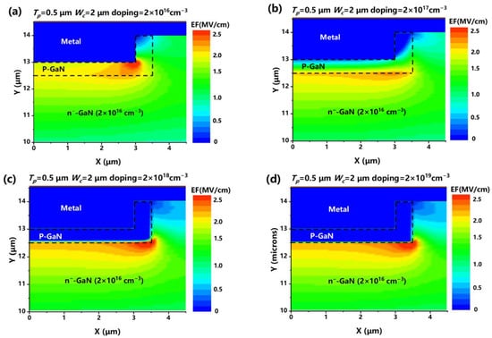
Figure 4.
Local 2-D electric field distributions of TJBS diodes with p-doping concentrations of (a) 2 × 1016 cm−3; (b) 2 × 1017 cm−3; (c) 2 × 1018 cm−3; and (d) 2 × 1019 cm−3 at 600 V reverse biased and a drift layer concentration of 2 × 1016 cm−3.
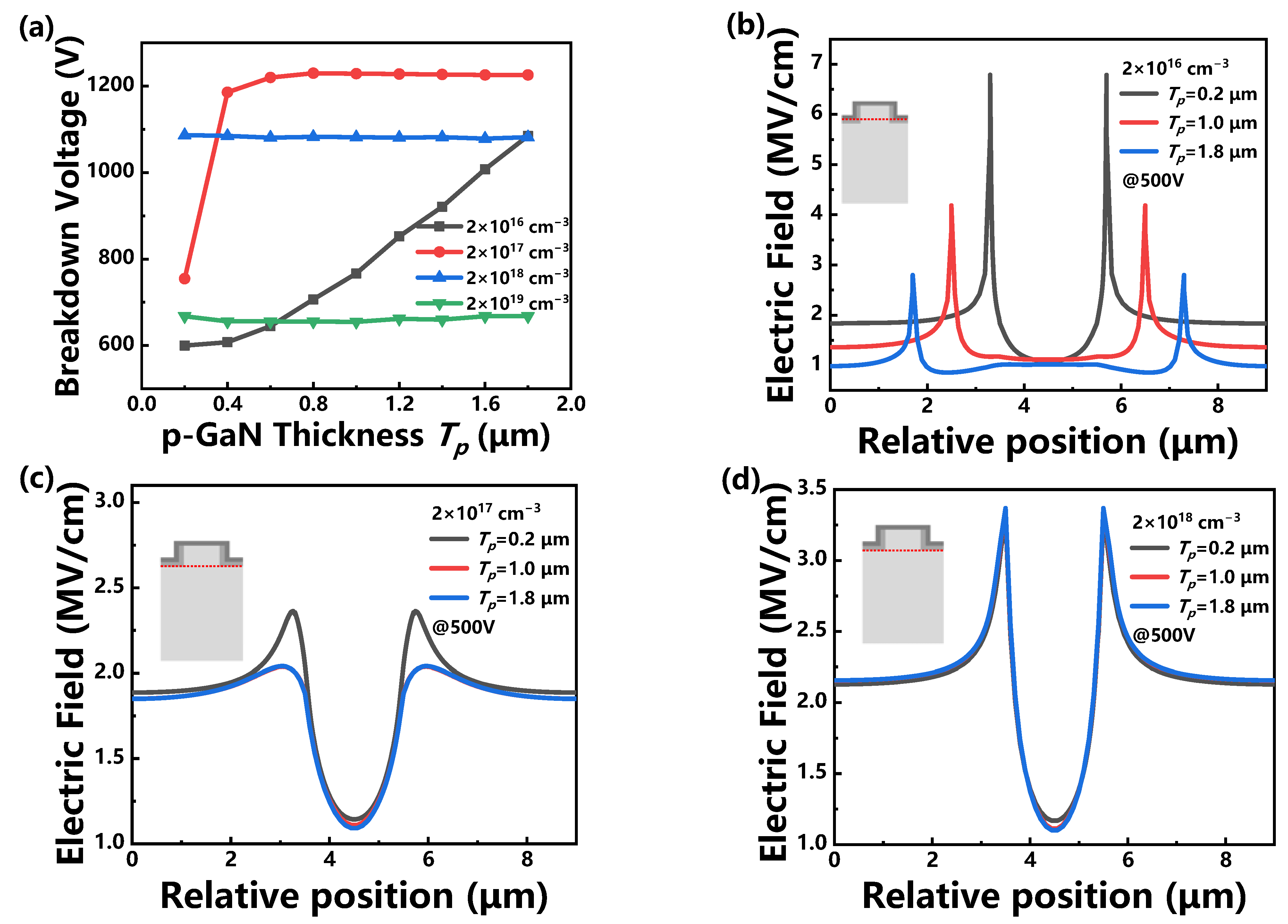
In addition to the doping concentration, the thickness of the p-GaN structure also plays a crucial role in the reverse characteristics of the TJBS diodes, as illustrated in Figure 5a. A stronger correlation between the breakdown voltage and the p-GaN thickness can be observed with a lower p-doping concentration. Specifically, with a p-doping concentration of 2 × 1016 cm−3, the breakdown voltage of the TJBS diodes increases monotonously with the p-GaN thickness. By increasing the p-doping concentration to 2 × 1017 cm−3, the breakdown voltage experiences a sharp increase with the p-GaN thickness before reaching a saturation at a p-GaN thickness of 0.4 μm. The breakdown voltage of the TJBS diodes remains constant with the p-GaN thickness when the p-doping concentration exceeds 2 × 1018 cm−3.
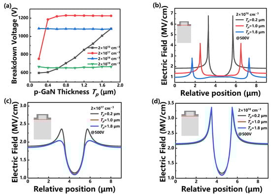
Figure 5.
(a) Breakdown voltage of TJBS diodes with different p-doping concentrations as a function of p-GaN thickness. When the drift layer concentration is 2 × 1016 cm−3, for different p-GaN thicknesses, the electric field profiles at 500 V along (b) the horizontal interface between metal and p-GaN and (c) the bottom of p-GaN correspond to p-doping concentrations of 2 × 1016 cm−3 and 2 × 1017 cm−3, respectively. (d) Electric field profiles at 500 V along the bottom of p-GaN for different p-GaN thicknesses when the p-doping concentration is 2 × 1018 cm−3.
Figure 5b,c shows the lateral 1-D electric field profile for the analysis of the breakdown mechanism of TJBS diodes with different p-GaN thicknesses. The premature breakdown occurs at the trench corner with a p-doping concentration of 2 × 1016 cm−3. Therefore, we extracted the electric field profile from the bottom of the trench, as shown by the dashed line in the inset of Figure 5b. To maintain a constant channel width (Wc), the width of the mesa (Wm) was varied in accordance with the thickness of the p-GaN (Tp). Thus, the position of the electric field peak also moves correspondingly. The peak value of the electric field gradually reduces with increased p-GaN thickness, effectively lowering the possibility of premature breakdown at the corner of the trench. As we increase the p-doping to 2 × 1017 cm−3, the electric field peaks at the corner of the p-GaN, as shown in Figure 5c. With increased p-GaN thickness from 0.2 μm to 1 μm, an obvious reduction in the peak electric field can be observed, while the 1-D electric field profile remained unchanged with further increased p-GaN thickness to 1.8 μm, which agrees with the aforementioned variation trend in the device breakdown voltage. With a p-doping concentration of 2 × 1018 cm−3, identical profiles for the 1-D electric field can be observed with different p-GaN thicknesses, which can well explain the constant breakdown voltage in Figure 5a.
3.2. Effect of p-GaN Spacing and Trench Depth on the Reverse Blocking Performances of TJBS Diodes
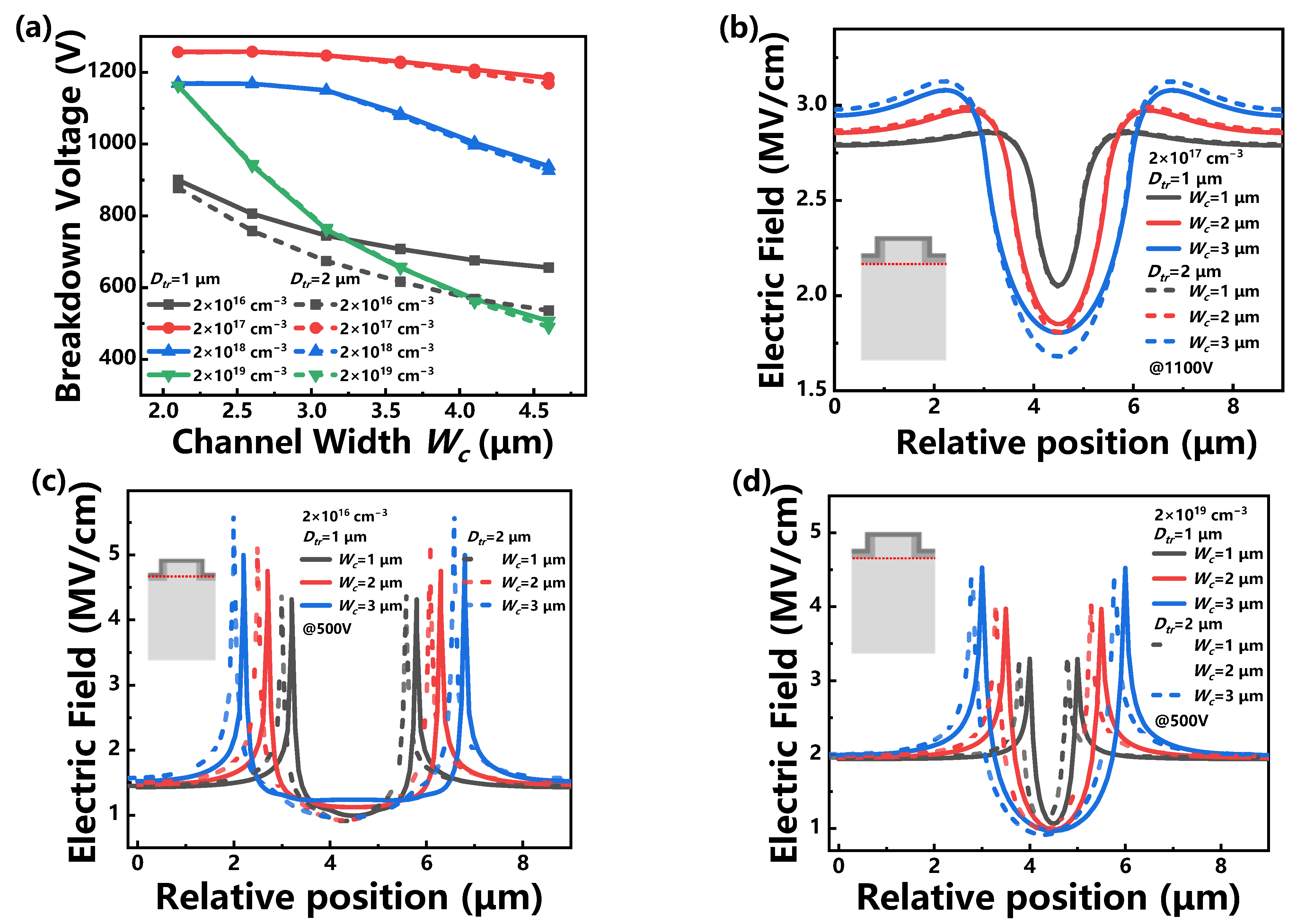
After addressing the effects of the p-GaN related design parameters (p-doping concentration and thickness), we then examine the influence of the geometrical dimensions (p-GaN spacing and trench depth) on the reverse characteristics of the TJBS diodes, as presented in Figure 6a. An inverse proportional relationship can be recorded between the breakdown voltage and the spacing between two adjacent p-GaN structures (Wc), regardless of the p-doping concentration. Note that a much sharper decrease of the breakdown value with Wc can be observed with a higher p-doping concentration of 2 × 1019 cm−3, resulting in the lowest breakdown voltage at a Wc of 3 μm. While the spacing has a significant effect on the reverse characteristics of the TJBS diodes, the trench depth exerts a minor influence on the breakdown voltage with a p-doping concentration higher than 2 × 1017 cm−3. With a lower p-doping concentration of 2 × 1016 cm−3, the distinction in the breakdown voltage is more pronounced between the TJBS diodes with a trench depth of 1 μm and 2 μm, respectively, which can be further enlarged with a larger Wc.
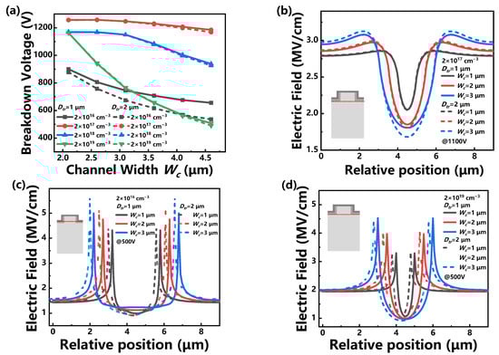
Figure 6.
(a) Breakdown voltages of TJBS diodes with different p-doping concentrations as a function of adjacent p-GaN spacing and its depth; (b) Electric field profiles at the bottom of p-GaN with a doping concentration of 2 × 1017 cm−3 and with different Dtr and Wc of TJBS at a reverse bias voltage of 1100 V; (c) Electric field profiles of TJBS diode with p-doping concentration of 2 × 1016 cm−3 and different Dtr and Wc along the interface between metal and p-GaN at 500 V; and (d) Electric field profiles at the bottom of p-GaN with a p-doping concentration of 2 × 1019 cm−3 at a reverse bias voltage of 500 V. To obtain a more obvious comparison the curves for Dtr = 2 μm in (c,d) are simultaneously shifted to the left by 0.2 μm.
The breakdown mechanism of the TJBS diodes is investigated by analyzing their 1-D electric field profiles at different Wc and Dtr. Figure 6b presents the lateral electric field profile along the bottom of the p-GaN with a doping concentration of 2 × 1017 cm−3. By increasing the Wc from 1 μm to 3 μm, the peak electric field value increases moderately, resulting in a slight reduction in the breakdown voltage of the TJBS diodes. An identical electric field profile can be observed for the TJBS diodes with different Dtr for a smaller Wc of 1 μm and 2 μm, while a larger Dtr can lead to an increased electric field with a larger Wc of 3 μm, which agrees with the slight drop of the breakdown voltage at a Wc of 3 μm, as shown in Figure 6a. With a relatively low p-doping concentration of 2 × 1016 cm−3 in Figure 6c, an increase in either Wc or Dtr is accompanied by a larger value of the electric field at the corner of the trench, causing a premature breakdown of the TJBS diodes. Under the condition of a high p-doping concentration of 2 × 1019 cm−3 in Figure 6d, a large proportion of the electric field concentrates at the edge of the p-GaN and increases dramatically with Wc, which can well explain the sharp decrease of the breakdown voltage in Figure 6a. Therefore, the geometrical parameters also play a crucial role in the reverse characteristics of the TJBS diodes, jointly determining the breakdown voltage of the devices with the p-doping concentration by tuning the distribution of the electric field.
3.3. Effect of Trench Bevel on the Blocking Performances and Forward Characteristics of TJBS Diodes
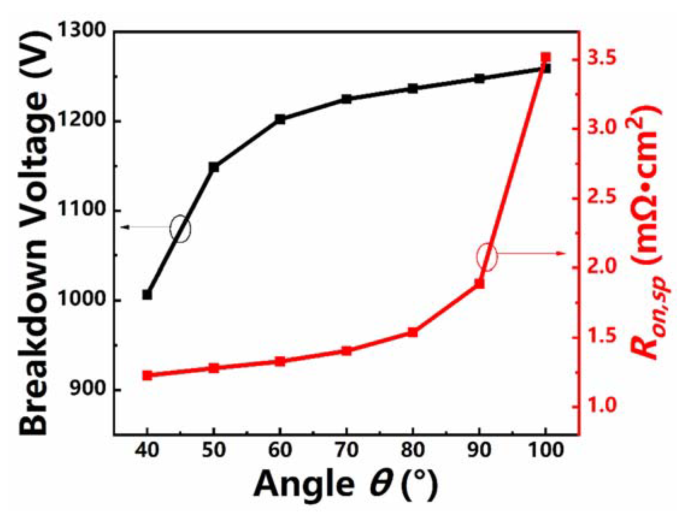
Based on the analysis above, an optimum reverse blocking performance of the TJBS diodes can be obtained with the p-doping concentration, Tp, Wc, and Dtr of 2 × 1017 cm−3, 0.8 μm, 1.5 μm, and 1 μm, respectively. Note that the key structural parameters are optimized with a trench angle (θ) of 90° [see Figure 1]. To develop a systematic study, we further investigated the effect of the angle on the reverse blocking performance and the forward characteristic of the TJBS diodes based on the optimized structure. As is shown in Figure 7, as θ increases from 40° to 100°, the reverse breakdown voltage increases monotonously from 1000 V to 1260 V, with a concomitant increase in on-resistance (Ron). Specially, when the value of θ changes from 90° to 100°, a sharp increase of the Ron can be observed from 1.8 mΩ·cm2 to 3.5 mΩ·cm2, which can be attributed to a narrower current conduction channel.
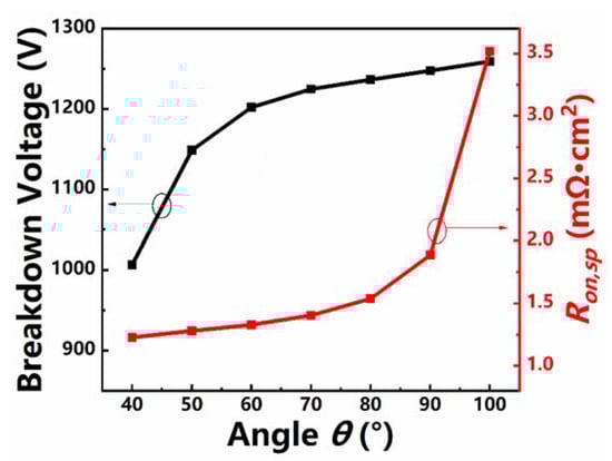
Figure 7.
Breakdown voltage and on-resistance of the TJBS diodes as a function of the variation of the angle (θ) of the trench slope.
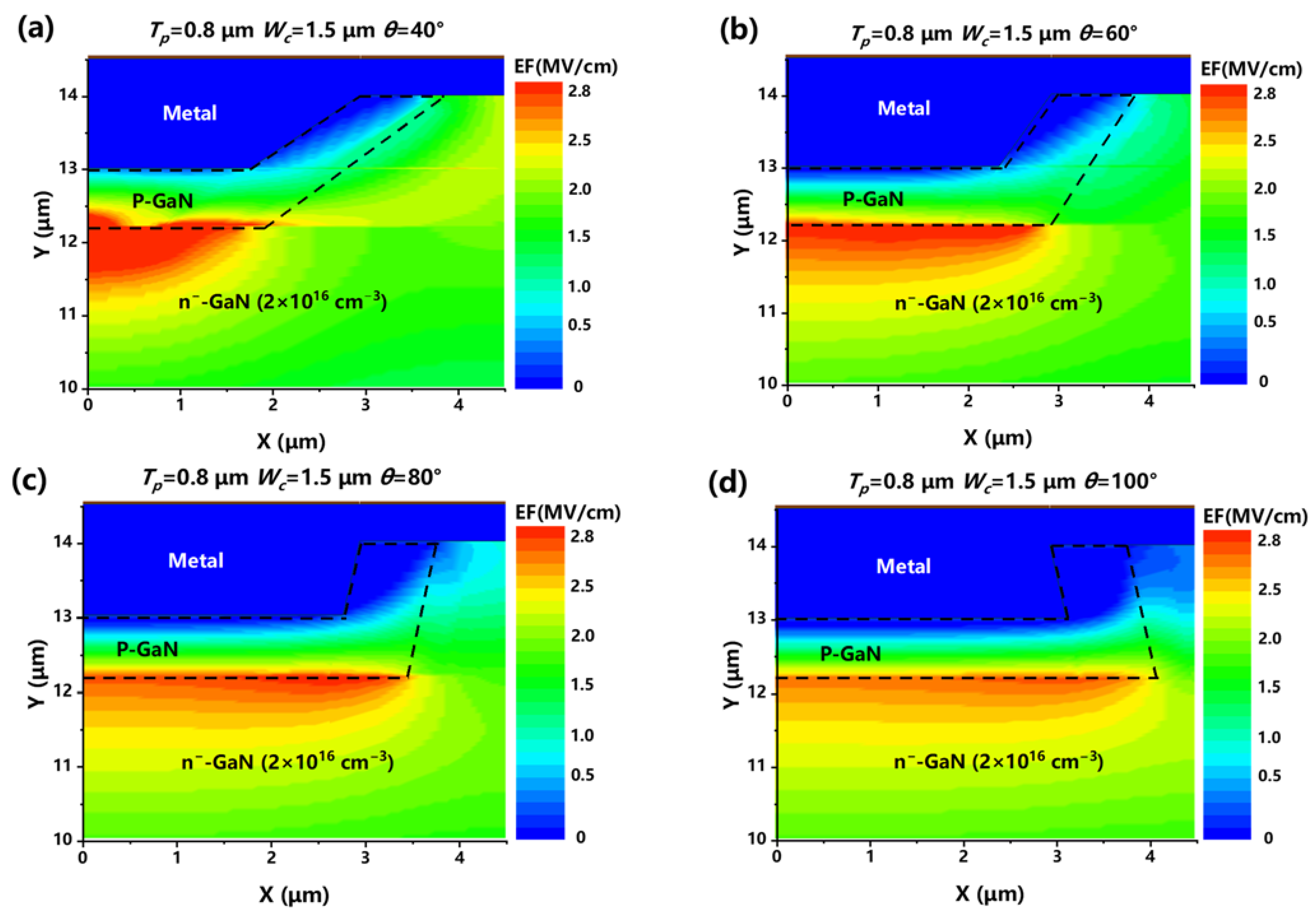
The reason for the increased breakdown voltage with a larger θ can be derived from the 2D electric field distribution in Figure 8. At a small θ of 40° in Figure 8a, the electric field crowding effect is locally significant at the bottom of the p-GaN. As θ gradually increases to 100° in Figure 8d, the electric field crowding effect can be effectively suppressed and the electric field exhibits a more uniform distribution at the bottom of the p-GaN, while an excellent electric field shielding effect can be formed under the Schottky interface. However, a larger θ leads to a smaller Wc between the adjacent p-GaN, thus results in a stronger depletion effect on the channel electric field by the adjacent pn junction.

Figure 8.
Local 2-D electric field distributions of TJBS diodes with a θ of (a) 40°; (b) 60°; (c) 80°; and (d) 100° with a p-doping concentration of 2 × 1017 cm−3 at a reverse bias of 1000 V.
To systematically explain the mechanism behind the variation trend of Ron with θ, the current path of the TJBS diodes under the forward conduction condition is analyzed in Figure 9, in which the current spreading region is represented by the grey part while the depletion region is marked with white color. For a TJBS diode, due to the presence of pn junction, the series resistance in the drift region can be divided into three different components, namely, the channel resistance (Rch), the spreading resistance (Rsp) and the drift region resistance (Rdr), respectively. According to the analysis in the References [21,30], on the condition that the angle of trench is not 90°, the angle (α) in Figure 9 can be expressed as
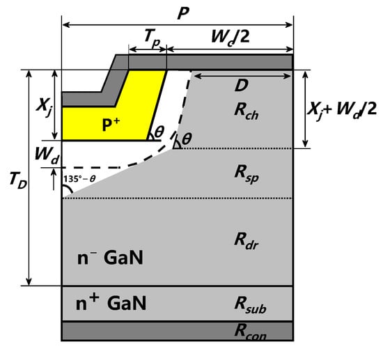
Figure 9.
Current path in TJBS diode used for on-state analysis.
The overall resistance Ron of device is determined by the resistive components, which can be given by
where Rsub and Rcon represent the substrate resistance and the ohmic contact resistance, which are determined by the conductivity of the selected substrate and the process of forming ohmic contact, respectively. In detail, specific Rch (Rch,sp), specific Rsp (Rsp,sp) and specific Rdr (Rdr,sp) can be derived as
where P is the width of the whole device cell, is the resistivity of the drift layer, and Xd, M, N are abbreviations used for ease of calculation and can be given by
Taking the adoption of the p+ structure in the TJBS diodes into account, the relationship between the forward voltage drop (VFS) and the current density for the Schottky barrier can be expressed as
where ΦB is the Schottky barrier height, q is the electron charge, k is the Boltzmann constant, T is the Kelvin temperature, and A* is the Richardson constant. represents the current density through the Schottky surface, which is proportional to the cell current density () by the following expression
where D is the width of the Schottky interface under the conduction path, which is related to the width of the channel (Wc) and the junction depletion region (Wd)
Wd can be derived from the following equation:
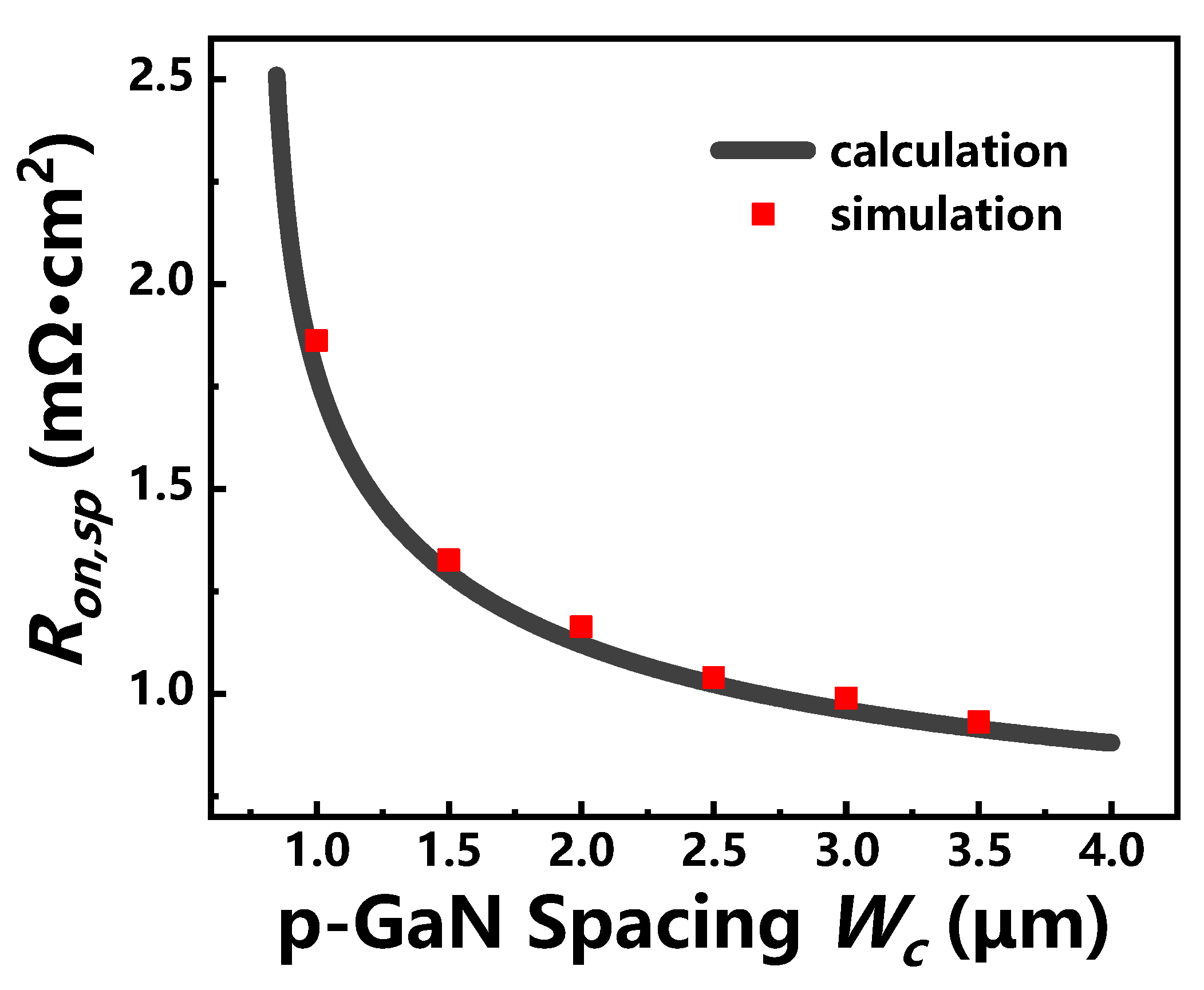
where , , and are the dielectric constant, the built-in potential difference, the applied forward bias, and the drift layer doping concentration, respectively. Furthermore, the simulated Ron of the TJBS diodes with θ of 60° in terms of Wc is presented in Figure 10, in which the curve of Ron calculated according to the proposed analytical calculation model is also shown. It can be seen that there is a favorable agreement between the calculation values and the simulation results, confirming the validity of the proposed analytical calculation model.

Figure 10.
Comparison of the specific on-resistance calculated from the resistance analysis model with the simulation results for TJBS diodes with θ = 60°.
The analytical model can be used for intuitively analyzing the variation of Ron and calculate the forward voltage drop (VFS) of the TJBS diodes, which can pave the way for the design of high performance TJBS diodes for a variety of applications.
For the purpose of experimentally demonstrating the TJBS diodes proposed in this work, a dry etching process is demanded to expose the bottom and sidewall of the trenches. The inevitably created defects during the etching process may induce undesirable traps for the TJBS diodes, which may result in increased reverse leakage and degrade the dynamic performance of the devices. Possible solutions involve wet etching by Tetra Methyl Ammonium Hydroxide (TMAH) [3,5]. In addition, it is not trivial to achieve uniform pn junctions at the sidewall of the etched mesas by ion implantation. A regrowth process of p-type GaN layer may be a feasible alternative way to achieve the proposed TJBS structure [31].
4. Conclusions
In summary, we report GaN vertical TJBS diodes and systematically investigate the impacts of the key design parameters on the reverse and forward characteristics. Compared with conventional PJBS diodes, the TJBS structure can suppress the electric field at the Schottky interface more effectively by taking advantage of the electric field shielding effect. We found that the electric field profile can be influenced by the doping concentration, thickness and spacing of p-GaN, as well as the depth and angle of the trench sidewalls. Furthermore, the effects of the cross-sectional profile on the forward characteristics of the TJBS diodes are investigated and the analytical model of the forward conduction is also developed. The results can pave the way towards a high-power, high-voltage, and low-loss GaN vertical Schottky barrier diodes for high-efficiency power system applications.
Author Contributions
Conceptualization, J.Y. and S.C.; methodology, J.Y. and H.C.; formal analysis, J.Y., S.C., H.C. and C.L.; writing—original draft preparation, J.Y.; writing—review and editing, S.L., H.F. and C.L.; supervision, C.L. All authors have read and agreed to the published version of the manuscript.
Funding
This research was funded in part the National Natural Science Foundation of China under Grant 62104135, in part by the Shenzhen Science and Technology Program under Grant JCYJ20210324141212030, in part by the Guangdong Basic and Applied Basic Research Foundation under Grant 2020A1515111018, in part by the Shandong Provincial Natural Science Foundation under Grant ZR2020QF079, and in part by the Qilu Young Scholar program under Grant 11500089963075.
Conflicts of Interest
The authors declare no conflict of interest.
References
- Millán, J.; Godignon, P.; Perpiñà, X.; Pérez-Tomás, A.; Rebollo, J. A Survey of Wide Bandgap Power Semiconductor Devices. IEEE Trans. Power Electron. 2014, 29, 21553. [Google Scholar] [CrossRef]
- Roccaforte, F.; Fiorenza, P.; Greco, G.; Nigro, R.L.; Giannazzo, F.; Iucolano, F.; Saggio, M. Emerging trends in wide band gap semiconductors (SiC and GaN) technology for power devices. Microelectron. Eng. 2018, 187, 66–77. [Google Scholar] [CrossRef]
- Liu, C.; Khadar, R.A.; Matioli, E. GaN-on-Si Quasi-Vertical Power MOSFETs. IEEE Electron Device Lett. 2018, 39, 71–74. [Google Scholar] [CrossRef]
- Khadar, R.A.; Floriduz, A.; Liu, C.; Soleimanzadeh, R.; Matioli, E. Quasi-vertical GaN-on-Si reverse blocking power MOSFETs. Appl. Phys. Express 2021, 14, 046503. [Google Scholar] [CrossRef]
- Liu, C.; Khadar, R.A.; Matioli, E. Vertical GaN-on-Si MOSFETs with Monolithically Integrated Freewheeling Schottky Barrier Diodes. IEEE Electron Device Lett. 2018, 39, 1034–1037. [Google Scholar] [CrossRef]
- Fu, H.; Huang, X.; Chen, H.; Lu, Z.; Baranowski, I.; Zhao, Y. Ultra-low turn-on voltage and on-resistance vertical GaN-on-GaN Schottky power diodes with high mobility double drift layers. Appl. Phys. Lett. 2017, 111, 152102. [Google Scholar] [CrossRef] [Green Version]
- Zhou, F.; Xu, W.; Ren, F.; Zhou, D.; Chen, D.; Zhang, R.; Zheng, Y.; Zhu, T.; Lu, H. High-Voltage Quasi-Vertical GaN Junction Barrier Schottky Diode with Fast Switching Characteristics. IEEE Electron Device Lett. 2021, 42, 974–977. [Google Scholar] [CrossRef]
- Khadar, R.A.; Floriduz, A.; Wang, T.; Matioli, E. p-NiO junction termination extensions for GaN power devices. Appl. Phys. Express 2021, 14, 071006. [Google Scholar] [CrossRef]
- Bian, Z.; Zhang, T.; Zhang, J.; Zhao, S.; Zhou, H.; Xue, J.; Duan, X.; Zhang, Y.; Chen, J.; Dang, K. Leakage mechanism of quasi-vertical GaN Schottky barrier diodes with ultra-low turn-on voltage. Appl. Phys. Express 2019, 12, 084004. [Google Scholar] [CrossRef]
- Hasegawa, K.; Nishio, G.; Yasunishi, K.; Tanaka, N.; Murakami, N.; Oka, T. Vertical GaN trench MOS barrier Schottky rectifier maintaining low leakage current at 200 °C with blocking voltage of 750 V. Appl. Phys. Express 2017, 10, 121002-1–121002-3. [Google Scholar] [CrossRef]
- Zhang, Y.; Sun, M.; Liu, Z.; Piedra, D.; Pan, M.; Gao, X.; Lin, Y.; Zubair, A.; Yu, L.; Palacios, T. Novel GaN trench MIS barrier Schottky rectifiers with implanted field rings. In Proceedings of the 2016 IEEE International Electron Devices Meeting (IEDM), San Francisco, CA, USA, 3–7 December 2016; pp. 10.2.1–10.2.4. [Google Scholar]
- Chen, S.; Chen, H.; Qiu, Y.; Liu, C. Systematic Design and Parametric Analysis of GaN Vertical Trench MOS Barrier Schottky Diode with p-GaN Shielding Rings. IEEE Trans. Electron Devices. 2021, 68, 5707–5713. [Google Scholar] [CrossRef]
- Hayashida, T.; Nanjo, T.; Furukawa, A.; Yamamuka, M. Vertical GaN merged PiN Schottky diode with a breakdown voltage of 2 kV. Appl. Phys. Express 2017, 10, 061003-1–061003-3. [Google Scholar] [CrossRef]
- Li, W.; Nomoto, K.; Pilla, M.; Pan, M.; Gao, X.; Jena, D.; Xing, H.G. Design and Realization of GaN Trench Junction-Barrier-Schottky-Diodes. IEEE Trans. Electron Devices 2017, 64, 1635–1641. [Google Scholar] [CrossRef]
- Zhang, Y.; Liu, Z.H.; Tadjer, M.J.; Sun, M.; Hatem, D.P.C.; Anderson, T.J.; Luna, L.E.; Nath, A.; Koehler, A.D.; Okumura, H.; et al. Vertical GaN Junction Barrier Schottky Rectifiers by Selective Ion Implantation. IEEE Electron Device Lett. 2017, 38, 1097–1100. [Google Scholar] [CrossRef]
- Koehler, A.D.; Anderson, T.J.; Tadjer, M.J.; Nath, A.; Feigelson, B.N.; Shahin, D.I.; Hobart, K.D.; Kub, F.J. Vertical GaN junction barrier Schottky diodes. ECS J. Solid State Sci. Technol. 2016, 6, Q10–Q12. [Google Scholar] [CrossRef]
- Zhou, F.; Xu, W.; Ren, F.; Zhou, D.; Chen, D.; Zhang, R.; Zheng, Y.; Zhu, T.; Lu, H. Demonstration of Avalanche and Surge Current Robustness in GaN Junction Barrier Schottky Diode with 600-V/10-A Switching Capability. IEEE Trans. Power Electron. 2021, 36, 12163–12167. [Google Scholar] [CrossRef]
- Hu, J.; Zhang, Y.; Sun, M.; Piedra, D.; Piedra, N.; Chowdhury, N.; Palacios, T. Materials and processing issues in vertical GaN power electronics. Mater. Sci. Semicond. Process 2018, 78, 75–84. [Google Scholar] [CrossRef] [Green Version]
- Narita, T.; Yoshida, H.; Tomita1, K.; Kataoka, K.; Sakurai, H.; Horita, M.; Bockowski, M.; Ikarashi, N.; Suda, J.; Kachi, T.; et al. Progress on and challenges of p-type formation for GaN power devices. J. Appl. Phys. 2020, 128, 090901. [Google Scholar] [CrossRef]
- Dou, W.; Song, Q.; Yuan, H.; Tanga, X.; Zhang, Y.; Zhang, Y.; Xiao, L.; Wang, L. Design and fabrication of high performance 4H-SiC TJBS diodes. J. Cryst. Growth 2020, 533, 125421. [Google Scholar] [CrossRef]
- Ren, N.; Wang, J.; Sheng, K. Design and Experimental Study of 4H-SiC Trenched Junction Barrier Schottky Diodes. IEEE Trans. Electron Devices 2014, 61, 2459–2465. [Google Scholar] [CrossRef]
- Konishi, K.; Kameshiro, N.; Yokoyama, N.; Shima, A.; Shimamoto, Y. Effect of trench structure on reverse characteristics of 4H-SiC junction barrier Schottky diodes. Jpn. J. Appl. Phys. 2017, 56, 121301-1–121301-6. [Google Scholar] [CrossRef]
- Oikawa, T.; Saijo, Y.; Kato, S.; Mishima, T.; Nakamura, T. Formation of definite GaN p-n junction by Mg-ion implantation to n--GaN epitaxial layers grown on a high-quality free-standing GaN substrate. Nucl. Instrum. Methods Phys. Res. Sect. B-Beam Interact. Mater. Atoms. 2015, 365, 168–170. [Google Scholar] [CrossRef]
- He, Y.; Lv, H.; Tang, X.; Song, Q.; Zhang, Y.; Han, C.; Zhang, Y.; Zhang, Y. Experimental study on the 4H-SiC-based VDMOSFETs with lightly doped P-well field-limiting rings termination. Solid-State Electron. 2017, 129, 175–181. [Google Scholar] [CrossRef]
- Crosslight Software Inc. APSYS 2018 and APSYS Technical Manuals. Available online: http://www.crosslight.com (accessed on 1 September 2020).
- Chynoweth, A.G. Ionization rates for electrons and holes in silicon. Phys. Rev. 1958, 109, 1537–1540. [Google Scholar] [CrossRef]
- Sundaramoorthy, V.K.; Nistor, I. Study of edge termination structures for high power GaN Schottky diodes. Phys. Status Solidi 2011, 8, 2270–2272. [Google Scholar] [CrossRef]
- Kozodoy, P.; DenBaars, S.P.; Mishra, U.K. Depletion region effects in Mg-doped GaN. J. Appl. Phys. 1999, 87, 770–775. [Google Scholar] [CrossRef]
- Han, S.; Yang, S.; Sheng, K. High-voltage and high-Ion/Ioff vertical GaN-on-GaN Schottky barrier diode with nitridation-based termination. IEEE Electron Device Lett. 2018, 39, 572–575. [Google Scholar] [CrossRef]
- Zhu, L.; Chow, T.P. Analytical Modeling of High-Voltage 4H-SiC Junction Barrier Schottky (JBS) Rectifiers. IEEE Trans. Electron Devices 2008, 55, 1857–1863. [Google Scholar] [CrossRef]
- Liu, H.; Fu, H.; Fu, K.; Alugubelli, S.R.; Su, P.-Y.; Zhao, Y.; Ponce, F.A. Non-uniform Mg distribution in GaN epilayers grown on mesa structures for applications in GaN power electronics. Appl. Phys. Lett. 2019, 114, 082102. [Google Scholar] [CrossRef] [Green Version]


Publisher’s Note: MDPI stays neutral with regard to jurisdictional claims in published maps and institutional affiliations. |
© 2022 by the authors. Licensee MDPI, Basel, Switzerland. This article is an open access article distributed under the terms and conditions of the Creative Commons Attribution (CC BY) license (https://creativecommons.org/licenses/by/4.0/).