Abstract
This paper presents a new electro-thermal coupling simulation method for evaluating the reliability of IGBT modules, which combines a numerical power loss model and a finite element model. To illustrate the method, a specific case of the Infineon FF50R12RT4 module operated with an SPWM signal is considered. Temperature and stress data are obtained and analyzed via electro-thermal simulation, and the service life of modules is calculated accordingly. The influence of ambient temperature and gate signal characteristics on power loss and service life of IGBT modules is discussed, which can be used for the optimization of work points. In this method, the effect of junction temperature on power loss is considered, and a more accurate electro-thermal simulation is achieved. The proposed method can be used to analyze the thermal and mechanical stresses of IGBT modules, predict the failure location, and assess the service life.
1. Introduction
Power converters play an important role in the electronic power industry, which is composed primarily of power semiconductor devices [1]. Common power semiconductor devices include a Giant Transistor (GTR), Metal Oxide Semiconductor Field Effect Transistor (MOSFET), Bipolar Junction Transistor (BJT), and Insulated Gate Bipolar Transistor (IGBT) [2]. IGBT combines the advantages of MOSFET and GTR, such as high input impedance, low output impedance, high current-carrying capacity, fast switching speed, and simple drive [3]. It is an ideal switching device and is widely used in power transmission, new energy generation, rail transportation, and other industries. The reliability of IGBT modules is crucial to the normal operation of electronic systems.
Studies show that temperature has a significant impact on IGBT failure [4,5]. Variations in ambient temperature and power loss during work cause temperature swings. Due to different coefficients of thermal expansion, temperature swings lead to thermomechanical stresses between the material layers inside the modules [6]. Under the long-term effect of thermomechanical stress, thermal fatigue is prone to occur in solder layers, and the bond wires are vulnerable to breaking and peeling off, which are the two most common types of failure [7]. The solder layer, bond wires, and chip metal layer were all found to be degraded in an aging experiment with ΔTj = 60 °C and Ta = 90 °C [8]. Other types of failure are die-attach degradation, severing of interconnections, delamination at bi-material interfaces, aluminum reconstruction, and cosmic-ray-induced failures [9,10].
Many failures of IGBT modules are related to thermal cycling. Thus, the analysis of the thermal characteristics of IGBT modules is vital for reliability assessment. Fast power cycling tests were conducted, and test results show the number of cycles to failure as a function of temperature changes for an IGBT single switch [11]. Bayerer et al. [12] proposed a model for the power cycling lifetime of IGBT modules that takes into account the effects of temperature swing, the diameter of bonding wire, power-on-time, current per wire bond, and many other factors. These models provide the basis for the life prediction of IGBT modules. In [13], a power dissipation lookup table and a second-order thermal R-C model were used to complete a fast electrothermal simulation of the converter. Predictions of inverter reliability for different conditions and designs were then obtained using Miner’s rule and the LESIT model to estimate the accumulated damage across the whole load cycle. A Cauer thermal model that can be used to represent the thermal behaviors of an IGBT power module was developed through FEM simulations [14]. A finite element model of the IGBT module was established, and a two-step indirect coupling electro-thermal-mechanical analysis was conducted to evaluate the wire bonding reliability of IGBT modules [15]. In order to improve the reliability and service life of IGBT modules, many thermal management methods have been proposed. The authors of [16] propose a strategy to design the reference junction temperature swing based on the distribution characteristics of a consumed lifetime and the thermal control efficiency. Similarly, a closed-loop junction temperature control system, which is able to reduce occurring temperature swings in order to reduce damage and extend the expected lifetime, is presented in [6]. Through electro-thermal analysis via finite element modeling, Ahsan et al. [9] proposed a driving strategy in which the switching frequency is adjusted based on power losses to mitigate stresses on the IGBT.
In order to precisely assess the reliability of IGBT modules, an electro-thermal coupling simulation method that combines a power loss model and a finite element model is presented in this paper. The power loss model is built on the energy loss curve and output characteristic curve, and the temperature dependence of power loss is also considered. Firstly, an accurate electro-thermal analysis of the IGBT module under specific working conditions is conducted. Subsequently, based on the temperature and stress data, the failure location is predicted, and the service life is calculated. Finally, the influence of ambient temperature and gate signal characteristics on power loss and service life of IGBT modules is discussed. The novel method proposed in this paper can be used for the optimization of work points and prediction of service life, which provides a practical guide for IGBT module reliability analysis.
2. Electro-Thermal Model and Simulation
2.1. Loss Determination
Damage produced from temperature swings is the primary cause of IGBT module failure [17]. The heat mainly comes from the power loss generated by chips during work. Therefore, a precise loss calculation is essential for temperature analysis, stress analysis, and reliability assessment. The power loss of the IGBT module is influenced by electrical parameters and junction temperature. In this paper, the Infineon FF50R12RT4 module is used as the object of study, and a mathematical model of power loss based on the carrier cycle is developed.
The classic half-bridge structure of the IGBT module is shown in Figure 1. The module consists of two IGBT chips and two freewheeling diodes (FWD). The IGBT and FWD chips are periodically switched on and off when the module is in operation. Therefore, they are the main source of loss.
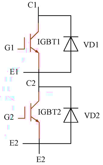
Figure 1.
The classic half-bridge structure of the IGBT module.
The power loss of the IGBT chip consists of the conduction loss , the turn-on loss , and the turn-off loss . The power loss of the FWD chip mainly includes the conduction loss and the switching loss . The cut-off loss for both is negligible.
The total power loss of the IGBT and FWD can be expressed as follows:
2.2. The Conduction Loss
The Sinusoidal Pulse Width Modulation (SPWM) technique is commonly used in inverters. In SPWM, a high-frequency triangular carrier wave is compared with the sinusoidal reference wave to produce gate signals to control the IGBT on and off, as shown in Figure 2.
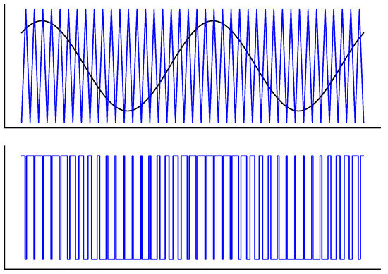
Figure 2.
Gate signal generation with SPWM.
With such gate signals, the switching frequency of chips is very high. The current flows periodically through IGBT chips and FWD chips. IGBT1 and VD2 operate during the first half of a modulating wave period, producing conduction loss and switching loss, and are in a cut-off state with no power loss during the second half.
The conduction loss of the IGBT chip during a switching cycle can be expressed as:
where is the switching cycle, is the collector-emitter voltage, and is the collector current.
Given the switching cycle of the IGBT module is extremely short and the inductive load’s time constant is significantly greater than the switching cycle, it could be assumed that and remain constant during one switching cycle [18]. Therefore, the conduction loss of the IGBT chip can be determined by the following equation:
where δ is the duty ratio of the IGBT chip. In SPWM, its expression is as follows:
where M is the modulation index, and and are the angular frequency and initial phase of the modulating wave, respectively.
Similarly, the conduction loss of the FWD chip during a switching cycle can be expressed as follows:
where is on-state voltage of the FWD.
The output characteristic curves of the IGBT module are shown in Figure 3. The on-state voltage of IGBT and FWD can be expressed as a linear function of threshold voltage and on-resistance [19]. The red and blue lines in Figure 3 represent the linear fitting results of output characteristic curves at different temperatures, respectively. Considering that the threshold voltage and on-resistance are affected by temperature, and can be described by the following equations:
where and are the rated on-state voltages at 25 °C for IGBT and FWD, respectively; and are the equivalent on-resistances at 25 °C for IGTB and FWD; and are the on-state voltage temperature coefficients of IGTB and FWD, respectively; and are the on-state resistance temperature coefficients of IGTB and FWD, respectively; and are the device junction temperatures.
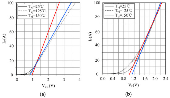
Figure 3.
Output characteristic curves of the IGBT module [20]. (a) Output characteristic curves of IGBT. (b) Output characteristic curves of FWD.
Substituting (7) and (8) into (4) and (6) gives the conduction loss for the IGBT and FWD as follows:
According to the output characteristic curves of the IGBT module, the parameters of the conduction loss can be calculated and shown in Table 1.

Table 1.
Parameters of the conduction loss.
2.3. The Switching Loss
The switching process of the IGBT module is extremely quick, complex, and influenced by many factors. Therefore, it is difficult to calculate the switching loss by simply multiplying the voltage and current. The datasheet of the IGBT module provides an - switching energy characteristic curve, from which the switching loss can be obtained easily.
Given the effect of the load current, the direct current (DC) terminal voltage, junction temperature, and grid resistance, the average turn-on and turn-off losses for the IGBT during a switching cycle can be expressed as follows:
where is the switching frequency; and are the energy losses during the turn-on and turn-off of the IGBT, which can be expressed as a function of the load current according to the switching energy curves; , , and represent the effect of DC voltage, chip junction temperature, and grid resistance on the switching loss, respectively.
According to the empirical formula, the DC voltage coefficient , the temperature coefficient , and the grid resistance coefficient in (11) and (12) can be expressed as follows [21,22]:
where is the DC voltage; is the reference voltage; is the empirical parameter, and its value is 1.4; is the junction temperature of IGBT; is the reference junction temperature; is the empirical parameter with a value of 0.003; is the reference grid resistance; and are the energy losses when the IGBT turns on and off with the reference gate resistance, obtained from the - curve of the IGBT in the module datasheet, as shown in Figure 4b.
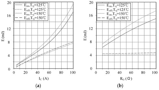
Figure 4.
Switching energy loss curves of IGBT [20]. (a) The influence of load current on switching loss. (b) The influence of gate resistance on switching loss.
Similarly, the switching loss of the FWD is expressed as follows:
where is the energy loss of FWD during turn-on and turn-off; and are empirical parameters, and their values are 0.6 and 0.006, respectively. is the switching energy loss of FWD with the reference grid resistance, obtained by consulting the switch energy loss curves of FWD from the datasheet. The other parameters are identical to those of the IGBT switching loss.
The parameters of the IGBT and FWD switching losses are shown in Table 2, and the functions fitted from the module switching energy loss curves are shown in Table 3.
Table 2.
Parameters of the switching loss.
Table 3.
Fitting results of switching energy loss curves.
2.4. Finite Element Thermal Model
The Infineon FF50R12RT4 module is used as the research object, and its internal structure is shown in Figure 5.
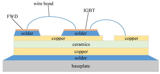
Figure 5.
Internal structure of the IGBT module.
The module consists of two parts, each containing an IGBT chip and an anti-parallel FWD chip. Its three-dimensional geometry model is constructed directly in COMSOL, as shown in Figure 6. The specific dimensional and material properties at a temperature of 25 °C are shown in Table 4 and Table 5. Temperature-dependent properties of materials are provided by the material library of COMSOL.
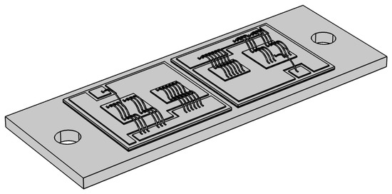
Figure 6.
Three-dimensional geometry model of the IGBT module.
Table 4.
Geometry parameters of IGBT module [23].
Table 5.
Material properties.
IGBT and FWD chips are set up as sources of heat because they produce power loss during operation. For thermal boundary conditions, an equivalent convection coefficient of 1500 W/(m2·K) is subjected to the bottom of the substrate, whereas other exposed surfaces are considered as heat insulation. For the displacement boundary condition, the bottom of the substrate and the screw holes are fixed completely, and the rest of the module is free. Thermal expansion occurs in all areas.
3. Electro-Thermal Simulation Validation
The power loss model is built in Matlab, and the heat transfer model is built in COMSOL. The schematic of the electro-thermal coupling simulation is shown in Figure 7.
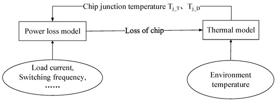
Figure 7.
Schematic of the electro-thermal coupling simulation.
The specific simulation conditions are set, as shown in Table 6.
Table 6.
Simulation parameters of model.
Figure 8 shows that the power loss of IGBT1 follows a sinusoidal pattern with the load current during the first half of the output current cycle, while the power loss of VD1 is zero. It is completely the contrary during the second half of the output current cycle. This is due to the current passing through IGBT1 and VD2 in the first half of the cycle and IGBT2 and VD1 in the second.
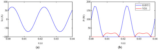
Figure 8.
(a) The waveform of output current Ic. (b) Simulation results of IGBT module power loss.
The junction temperatures of IGBT and FWD in the first four seconds are shown in Figure 9 and Figure 10. The IGBT module accumulates heat during this period, and the junction temperatures rise. The module converges to thermal equilibrium after about 15 s, where the junction temperatures fluctuate around the average junction temperature. The reason for the phenomenon is that the current periodically flows through the IGBT and FWD. The chip produces a loss, and the junction temperature rises when a current is flowing through it; conversely, when no current is flowing through it, the chip enters the cooling stage.
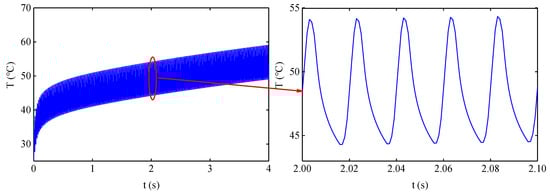
Figure 9.
Junction temperature of IGBT1.
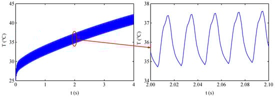
Figure 10.
Junction temperature of VD1.
The temperature fluctuations of different components in the IGBT module are shown in Figure 11. It is evident that the temperatures and temperature fluctuations of the bonding wire, chip, and upper solder layer are much higher than those of other sections because chips are the source of heat and are directly connected to the bond wire and higher solder layer. Therefore, these three components are likely to suffer more damage at work.
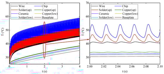
Figure 11.
Temperature fluctuations of different components in the IGBT module.
A half-bridge circuit with the same parameters as the model above is built in PLECS, a professional power electronics simulation software. The simulation results of both are shown in Table 7.
Table 7.
Model simulation parameters.
The relative errors of the data in Table 7 are calculated and found to be below 5%, which indicates that the model has high accuracy.
4. Results and Reliability Analysis
An electro-thermo-mechanical analysis is performed according to the simulation conditions in Table 6. The results of the temperature and stress of the IGBT module at the time of 17 s are shown in Figure 12 and Figure 13. At this moment, the module has converged to a thermal equilibrium where heat generation and heat dissipation are equal, and the junction temperature fluctuates in a specific range.
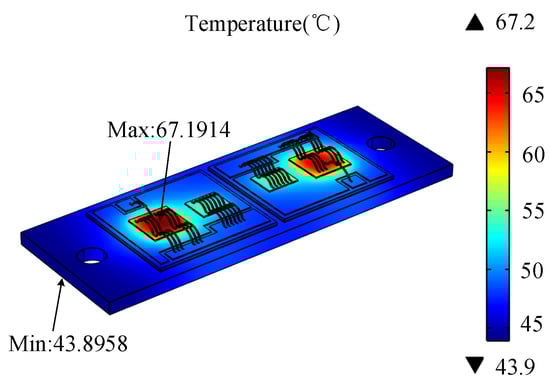
Figure 12.
VD1 junction temperature curve.
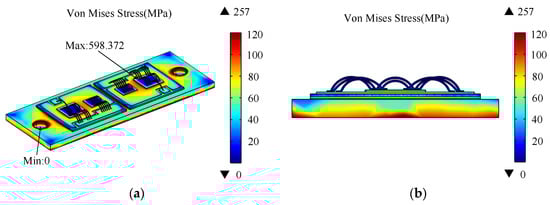
Figure 13.
Stress distribution of the IGBT module. (a) The entire module. (b) Section of each layer.
As seen from Figure 12, as the main source of heat, the temperature of IGBT chips is much higher than in other areas, suggesting that the area around the chips may be subject to high thermal stress.
Figure 13 shows the specific stress distribution of the module, and it can be seen that the layers and bond wires of the IGBT module are subject to thermal stress. However, the magnitude of the thermal stress varies from one part to another due to temperature, material properties, and constraint conditions. Overall, the stresses on the bottom of the substrate, the screw holes, the area around chips, the solder layer, and bond wire pins are higher, especially at bond wire pins.
Figure 14, Figure 15 and Figure 16 show the stress distribution of the solder layers and bonding wires. The stresses at the bottom edge of the upper solder and the edge of the lower solder are relatively high compared to other areas, with maximum stresses of up to 142.98 MPa and 215.81 MPa, which will lead to the initiation and development of cracks from the edge of the solder layer and thus the failure of the module. The maximum stress on the IGBT module is at the bonding wire pins, with a value of 598.372 MPa. At such high stresses over a long period of time, the bonding wire can easily fall off and lead to module failure.

Figure 14.
The stress distribution of top and bottom surfaces of the upper solder layer.
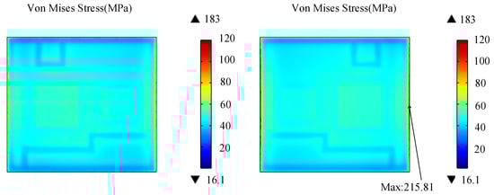
Figure 15.
The stress distribution of top and bottom surfaces of the lower solder layer.
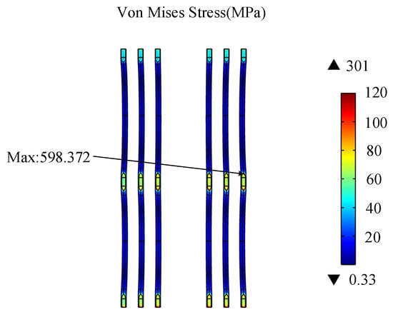
Figure 16.
The stress distribution of wire bonds.
To assess the service life of the IGBT module, the cumulative damage is calculated. The random loads to which the IGBT modules are subjected are almost always distributed in the range of high-cycle fatigue; Miner’s linear cumulative damage theory is chosen as the basis for calculating the cumulative damage. By analyzing the historical junction temperature data, extracting the characteristic parameters using the cycle counting method, and combining it with the power cycle diagram, the cumulative damage is calculated.
A model commonly used to describe power cycle diagrams is the Bayerer lifetime model from Infineon. The model was built by analyzing a large amount of power cycle data from different module technologies collected over many years at various conditions. The total number of cycles to failure can be expressed as follows [16]:
where K = 9.3 × 10¹⁴, = −4.416, = 1285, = −0.463, = −0.716, = −0.761, = −0.5, , and is the magnitude and minimum of the junction temperature, is power-on-time, I is current per wire, V is blocking voltage of the chip(×100 V), and D is the diameter of the bonding wire.
Because of nonuniform temperature fluctuations, rainflow cycle counting, a method that can account for the number of cycles of each combination of mean and range, is applied to explore its effect on service life. The junction temperature curve of the IGBT module in a steady state at the working condition in Table 6 is shown in Figure 17. The resulting rainflow matrix of Figure 17, namely the magnitude—mean—number of cycles distribution, is shown in Figure 18.
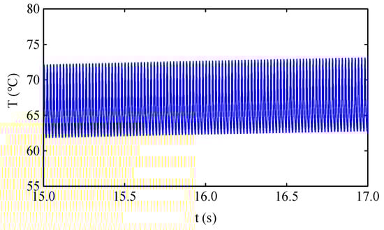
Figure 17.
The junction temperature of the IGBT module.
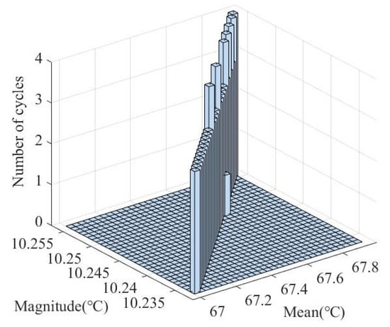
Figure 18.
The temperature load spectrum of the IGBT module.
With (18), the total cumulative damage to the IGBT module caused by the temperature loads from the 15th second to the 17th second can be obtained as follows:
When the cumulative damage level reaches 1, the module will fail. The service life of the IGBT module at the working condition in Table 6 is as follows:
The service life of the IGBT module is different under different working conditions. To study the effect of working conditions on the lifetime, simulations of different parameters are carried out.
By modifying the ambient temperature in the electrothermal model, its influence on the life of the IGBT module is explored. Table 8 displays the results with the environmental temperature set at 25 °C, 35 °C, and 45 °C, respectively.
Table 8.
Simulation results of different environmental temperatures.
As seen from Table 8, with the increase in ambient temperature, the power loss of the IGBT module increases, making the change of the mean junction temperature greater than that of the ambient temperature and the range of temperature fluctuation larger, and the cumulative damage of the IGBT module also increases. When the ambient temperature is 35 °C and 45 °C, the cumulative damage of the IGBT module is 1.25 and 1.56 times that of T = 25 °C, respectively. The service life of the IGBT module is reduced to 80% and 64% of that at T = 25 °C, which shows that the change in ambient temperature seriously affects the service life of the IGBT module. Therefore, a good cooling device can be used to reduce the temperature of the working environment and improve the service life of the IGBT module.
Generally, the on and off periods of the IGBT in the inverter are controlled by the gate signal, and the characteristics of the gate signal influence the service life of the IGBT module. The generation of the gate signal is shown in Figure 2. The frequency of the triangular carrier wave, the frequency of the modulating wave, and the modulation index determine the characteristics of the gate signal and then influence the working process and service life of IGBT modules. The frequency of the triangular carrier determines the switching frequency of IGBT modules. The frequency of the sinusoidal reference wave determines the frequency of the output current. The modulation index controls the amplitude of output voltage. To explore the impact of these factors on the lifetime of IGBT modules, simulations are carried out after modifying the parameters of the model.
Carrier frequencies are set at 3 KHz, 4 KHz, and 5 KHz, respectively. The simulation results are shown in Table 9. The simulation results when the frequency of the sinusoidal reference wave is set to 50 Hz, 100 Hz, and 150 Hz are shown in Table 10. Table 11 shows the simulation results for the modulation index of 0.7, 0.8, and 0.9, respectively.
Table 9.
Effects of carrier frequency on the lifetime of IGBT module.
Table 10.
Effects of modulating wave frequency on the lifetime of IGBT module.
Table 11.
Effects of modulation index on the lifetime of IGBT module.
As seen from Table 9, Table 10 and Table 11, the characteristics of the gate signal greatly affect the service life of the IGBT module. The service life of the IGBT module decreases with the increase in carrier frequency and modulation index and increases with the rise of modulating wave frequency. The increase in carrier frequency leads to an increase in IGBT switching frequency, so the power loss increases and the service life decreases. The increasing frequency of the modulated wave reduces the power loss and leads to a shorter heating and cooling time for IGBT, so the mean and range of temperature fluctuations are reduced. The rise of the modulation index makes the output voltage and current higher, thus affecting the service life of the IGBT module. Therefore, according to the working condition of IGBT modules, a reasonable reduction in carrier frequency and modulation index and an increase in modulating wave frequency can reduce power loss and improve its service life.
5. Conclusions
An electro-thermal coupling simulation method, which uses a numerical model of power loss and a finite element model, is proposed in this paper. With this method, the impact of temperature is considered, allowing for more precise temperature and stress distribution. A thermal and stress analysis is conducted, and the simulation data match those of PLECS. The results show that failure of the IGBT module may start at the bonding wire pins and the solder layer’s edge. Then, the application of rainflow cycle counting and the Bayerer model to calculate the service life is presented, and the reliability of IGBT modules for different conditions is discussed by estimating the accumulated damage and service life. It can be seen that the reliability of the IGBT module decreases with the increase in ambient temperature, carrier frequency, and modulation index and increases with the rise of modulating wave frequency.
Author Contributions
Conceptualization, X.Z.; Methodology, X.Z.; Software, M.L.; Validation, X.Z.; Formal analysis, X.Z.; Investigation, S.L. and H.D.; Resources, M.L. and H.D.; Data curation, S.L.; Writing—original draft, X.Z.; Writing—review & editing, X.Y. and Y.H.; Supervision, X.Y.; Project administration, Y.H.; Funding acquisition, Y.H. All authors have read and agreed to the published version of the manuscript.
Funding
This research received no external funding.
Data Availability Statement
Data are available from the authors upon reasonable request.
Conflicts of Interest
The authors declare no conflict of interest.
References
- Ronanki, D.; Singh, S.A.; Williamson, S.S. Comprehensive Topological Overview of Rolling Stock Architectures and Recent Trends in Electric Railway Traction Systems. IEEE Trans. Transp. Electrif. 2017, 3, 724–738. [Google Scholar] [CrossRef]
- Durand, C.; Klingler, M.; Coutellier, D.; Naceur, H. Power Cycling Reliability of Power Module: A Survey. IEEE Trans. Device Mater. Reliab. 2016, 16, 80–97. [Google Scholar] [CrossRef]
- Oh, H.; Han, B.; McCluskey, P.; Han, C.; Youn, B.D. Physics-of-Failure, Condition Monitoring, and Prognostics of Insulated Gate Bipolar Transistor Modules: A Review. IEEE Trans. Ind. Appl. 2015, 30, 2413–2426. [Google Scholar] [CrossRef]
- Blaabjerg, F. Design for Reliability in Power Electronic Systems. In Proceedings of the 2018 20th European Conference on Power Electronics and Applications, Riga, Latvia, 17–21 September 2018; p. 1. [Google Scholar]
- Choi, U. Studies on IGBT Module to Improve the Reliability of Power Electronic Systems. Ph.D. Dissertation, Aalborg University, Aalborg, Denmark, 2016. [Google Scholar] [CrossRef]
- Ruthardt, J.; Klinkhammer, A.; Marx, P.; Ziegler, P.; Nitzsche, M.; Sharma, K.; Roth-Stielow, J. Lifetime Extension of Power Semiconductor Devices by Closed-Loop Junction Temperature Control. In Proceedings of the 2021 23rd European Conference on Power Electronics and Applications, Ghent, Belgium, 6–10 September 2021; pp. 1–10. [Google Scholar] [CrossRef]
- Smet, V.; Forest, F.; Huselstein, J.-J.; Richardeau, F.; Khatir, Z.; Lefebvre, S.; Berkani, M. Ageing and Failure Modes of IGBT Modules in High-Temperature Power Cycling. IEEE Trans. Ind. Electron. 2011, 58, 4931–4941. [Google Scholar] [CrossRef]
- Choi, U.-M.; Blaabjerg, F.; Jorgensen, S. Study on Effect of Junction Temperature Swing Duration on Lifetime of Transfer Molded Power IGBT Modules. IEEE Trans. Power Electron. 2017, 32, 6434–6443. [Google Scholar] [CrossRef]
- Ahsan, M.; Hon, S.T.; Batunlu, C.; Albarbar, A. Reliability Assessment of IGBT Through Modelling and Experimental Testing. IEEE Access. 2020, 8, 39561–39573. [Google Scholar] [CrossRef]
- Busca, C.; Teodorescu, R.; Blaabjerg, F.; Munk-Nielsen, S.; Helle, L.; Abeyasekera, T.; Rodriguez, P. An overview of the reliability prediction related aspects of high power IGBTs in wind power applications. Microelectron. Reliab. 2011, 51, 1903–1907. [Google Scholar] [CrossRef]
- Held, M.; Jacob, P.; Nicoletti, G.; Scacco, P.; Poech, M.-H. Fast power cycling test of IGBT modules in traction application. In Proceedings of the Second International Conference on Power Electronics and Drive Systems, Singapore, 26–29 May 1997; pp. 425–430. [Google Scholar] [CrossRef]
- Bayerer, R.; Herrmann, T.; Licht, T.; Lutz, J.; Feller, M. Model for Power Cycling lifetime of IGBT Modules—Various factors influencing lifetime. In Proceedings of the 5th International Conference on Integrated Power Electronics Systems, Nuremberg, Germany, 11–13 March 2008; pp. 1–6. [Google Scholar]
- Bryant, A.T.; Mawby, P.A.; Palmer, P.R.; Santi, E.; Hudgins, J.L. Exploration of Power Device Reliability Using Compact Device Models and Fast Electrothermal Simulation. IEEE Trans. Ind. Appl. 2008, 44, 894–903. [Google Scholar] [CrossRef]
- Tang, C.; Thiringer, T. Thermal modelling of a mutlichip IGBT power module. In Proceedings of the 2019 21st European Conference on Power Electronics and Applications, Genova, Italy, 3–5 September 2019; pp. P.1–P.8. [Google Scholar] [CrossRef]
- Bie, X.; Qin, F.; An, T.; Zhao, J.; Fang, C. Numerical simulation of the wire bonding reliability of IGBT module under power cycling. In Proceedings of the 2017 18th International Conference on Electronic Packaging Technology, Harbin, China, 16–19 August 2017; pp. 1396–1401. [Google Scholar] [CrossRef]
- Zhang, J.; Du, X.; Qian, C.; Ye, Y.; Zhou, J. Design of Reference Junction Temperature Swing of Power Module for Thermal Management. IEEE Trans. Power Electron. 2023, 38, 1132–1143. [Google Scholar] [CrossRef]
- Du, B.; Hudgins, J.L.; Santi, E.; Bryant, A.T.; Palmer, P.R.; Mantooth, H.A. Transient Electro-thermal Simulation of Power Semiconductor Devices. IEEE Trans. Power Electron. 2010, 25, 237–248. [Google Scholar] [CrossRef]
- Zhou, Z.; Khanniche, M.; Igic, P.; Kong, S.; Towers, M.; Mawby, P. A fast power loss calculation method for long real time thermal simulation of IGBT modules for a three-phase inverter system. In Proceedings of the 2005 European Conference on Power Electronics and Applications, Dresden, Germany, 11–14 September 2005; pp. 9–10. [Google Scholar] [CrossRef]
- Graovac, D.; Pürschel, M. IGBT power losses calculation using the data-sheet parameters. Infineon Appl. Note 2009, 1, 1–16. [Google Scholar]
- Infineon. Available online: https://www.infineon.com/dgdl/Infineon-FF50R12RT4-DS-v02_00-en_cn.pdf?fileId=db3a30433db6f09f013dcac65a1e5441 (accessed on 20 July 2022).
- Nicolai, U.; Wintrich, A. Determining Switching Losses of SEMIKRON IGBT Modules. SEMIKRON Application Note, AN. 2014; 1403. [Google Scholar]
- van der Broeck, C.H.; Ruppert, L.A.; Lorenz, R.D.; De Doncker, R.W. Methodology for Active Thermal Cycle Reduction of Power Electronic Modules. IEEE Trans. Power Electron. 2019, 34, 8213–8229. [Google Scholar] [CrossRef]
- Huang, X.; Guo, H. Stress-strain Analysis of IGBT Modules Based on Finite Element Simulation. Precise Manuf. Autom. 2017, 211, 22–25+40. [Google Scholar] [CrossRef]
Disclaimer/Publisher’s Note: The statements, opinions and data contained in all publications are solely those of the individual author(s) and contributor(s) and not of MDPI and/or the editor(s). MDPI and/or the editor(s) disclaim responsibility for any injury to people or property resulting from any ideas, methods, instructions or products referred to in the content. |
© 2023 by the authors. Licensee MDPI, Basel, Switzerland. This article is an open access article distributed under the terms and conditions of the Creative Commons Attribution (CC BY) license (https://creativecommons.org/licenses/by/4.0/).