1. Introduction
Internet of things (IoT) represents the concept of the communication between plenteous limited-power devices from various environments over a large-scale interconnected network without human involvement [
1]. Over the last few years, the IoT has been successfully deployed in diverse fields, such as intelligent environment, medical care, and transportation logistics [
1,
2].
With the anticipated evolution of the IoT market, the number of IoT devices has remarkably increased worldwide from 15.41 billion in 2015 to 23.14 billion in 2018, and it is expected to extend to 75.44 billion in 2025 [
3]. Thus, many communication protocols and standards have been recently developed to support a wide range of IoT applications. These protocols and standards, such as near-field communication (NFC), ZigBee, low-energy Bluetooth (BLE), and wireless-fidelity (Wi-Fi), are mostly dedicated to short-range applications [
4]. On the other hand, new low-power wide-area (LPWA) technologies have been developed to achieve wide-range communications, such as long-range wide area network (LoRaWAN), Sigfox, and weightless special interest group (SIG), that all operate in the unlicensed spectrum and have massive connectivity but require building new infrastructures [
4,
5]. Moreover, the cellular systems have been considered potential solutions to provide massive connectivity for machine-type communication (MTC) devices. Therefore, the 3rd Generation Partnership Project (3GPP) has introduced a new cellular technology standard known as narrowband internet of things (NB-IoT) to support the IoT applications [
6,
7].
The NB-IoT operates in a licensed spectrum, as it is based on the 3GPP long-term evolution (LTE), and contrary to other unlicensed LPWA technologies, the same infrastructure of LTE is utilized in NB-IoT [
8]. Furthermore, most features of LTE are inherited in NB-IoT, minimizing the complexity of LTE channels and signals to meet the constraints of low power and low cost in NB-IoT. Additionally, the number of these channels is decreased to fit the new frame structure of NB-IoT. The LTE protocol stacks in the evolved node B (eNB) and the user equipment (UE) are deployed in NB-IoT with a significant reduction in each layer’s functionalities [
5,
6].
The NB-IoT system is designed to occupy a bandwidth of 180 kHz, corresponding to one LTE physical resource block (PRB), which is deployed in three possible operation modes defined by 3GPP to ensure the coexistence with LTE carriers without decaying the LTE performance. These operation modes are in-band mode, guard-band mode, and standalone mode (in the liberated GSM channels) [
9]. Furthermore, the number of repetitions reaches up to 128 and 2048 repetitions in uplink and downlink, respectively, and that indeed improves the coverage [
7].
A detailed description of the main building blocks of the narrowband physical uplink shared channel (NPUSCH) transmitter and narrowband physical downlink shared channel (NPDSCH) receiver as specified by 3GPP standard is provided in this work. In addition, experimental results, including area utilization, power consumption, and clock latency of an FPGA hardware implementation of both NPUSCH and NPDSCH channels, are presented. The narrowband physical shared channels are responsible for the delivery of both user plane data as well as control information. However, only user plane data processing is discussed in this work.
The main contributions of this work can be listed as follows:
Chain integration is performed between the uplink transmitter and downlink receiver, including the base station model between them.
A whole chain results for bit error rate (BER) versus signal-to-noise ratio (SNR), and it is compared with the ideal case.
The whole chain is synthesized and implemented on the FPGA, which acts as a UE model.
Mimic the reality by building a prototype using two FPGAs connected to USRPs to serve as the UEs.
Several hardware techniques are adopted to reduce power consumption while meeting all of the 3GPP standard requirements.
An in-depth explanation is given of the hardware architecture of each block of the whole communication blocks, which paves the way to further work on the hardware implementation of the NB-IoT transceiver chain.
The remainder of the paper is organized as follows.
Section 2 describes the detailed design and implementation of both the NPUSCH transmitting chain and the NPDSCH receiving chain. The system integration with MATLAB and register transfer level (RTL), as well as the implementation on field programmable gate array (FPGA) are presented in
Section 3. The NB-IoT system architecture and hardware components are presented in
Section 4. The system implementation, including the hardware set-up, is depicted in
Section 5. At last,
Section 6 concludes this work.
2. NB-IoT System Detailed Design and Implementation
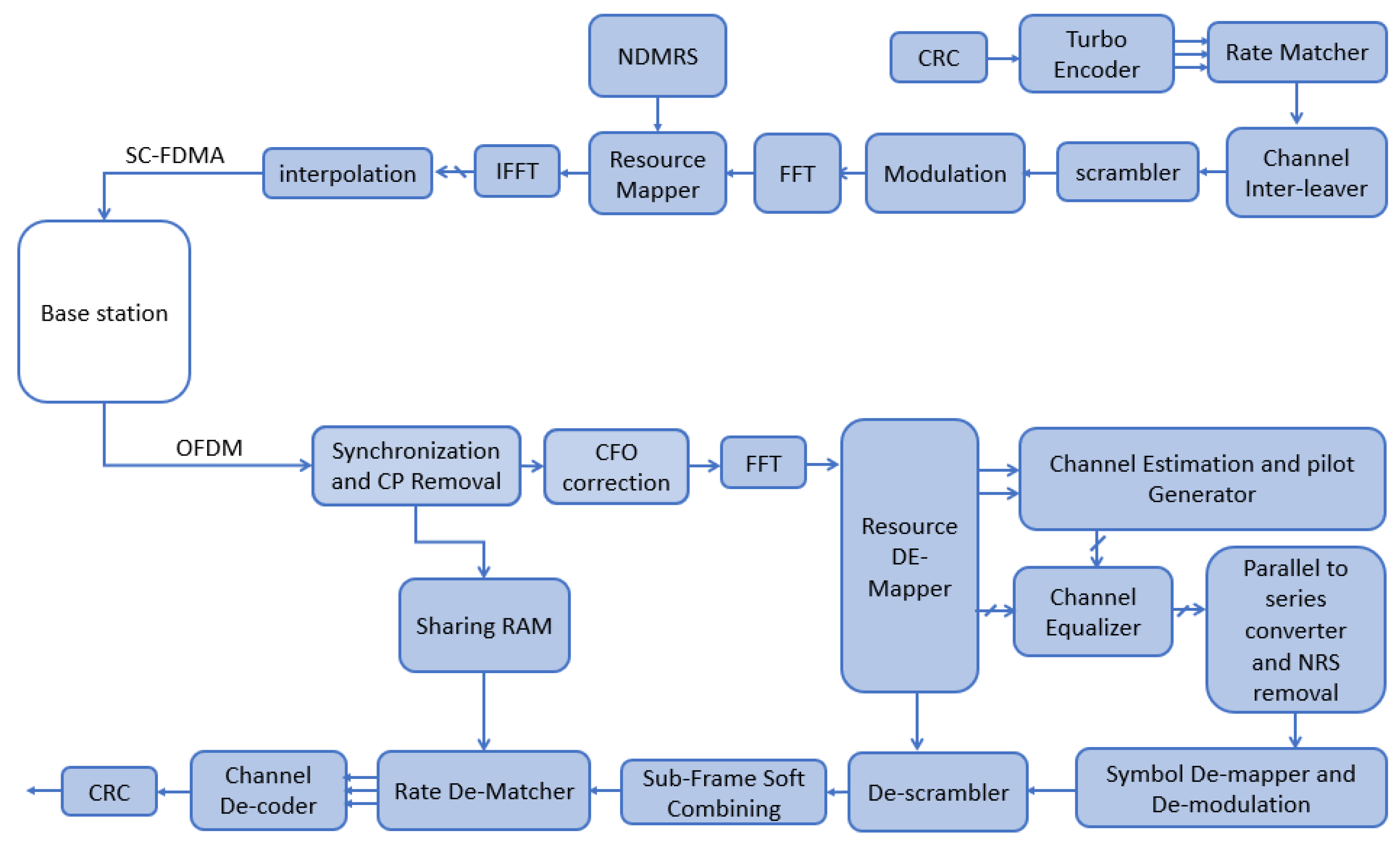
As illustrated in
Figure 1, the implemented NB-IoT system consists of two main parts as follows:
Figure 1.
Detailed block diagram of the NB-IoT transceiver.
Figure 1.
Detailed block diagram of the NB-IoT transceiver.
2.1. NPUSCH Transmitter Chain Implementation
In the uplink, the physical (PHY) layer receives a data transport block of a specified size from the MAC layer along with other upper layer parameters. The maximum transport block size TBS
max for NB-IoT is 2536 bits [
9]. The following subsections present the detailed implementation of each block in the transmitting chain.
2.1.1. Cyclic Redundancy Check (CRC)
The CRC is an error detection technique in which a checksum is generated and appended to the payload. In NB-IoT, the checksum (CRC bits) is 24 bits, generated by 24 registers and XORs according to the following polynomial [
10]:
As shown in
Figure 2, the CRC block is implemented as a shift register with the length of the CRC polynomial with the input data stream connected to the least significant flip-flop. The flip-flops that correspond by location to the ones in the CRC polynomial are connected to XORs to be XOR-ed with ones. In the meantime, multiplexers are placed to decide whether the register content or the XOR output will be passed to the next block [
10,
11].
2.1.2. Turbo Encoder
In recent years, turbo codes are the most potentially leading development in coding theory, as introducing turbo codes has provided a new way to look at the problem of constructing good codes and decoding them with low complexity. Due to the performance of turbo codes, which is close to the Shannon limit, this coding technique is used in various storage and communication systems to help the receiver correct the received data [
13]. The turbo encoder, which is recommended by 3GPP standardization for NB-IoT communication systems, consists of two recursive systematic convolutional encoders, which are usually identical but not necessary. Both convolutional encoders comprise three shift registers XOR-ed with the polynomials in (
3) and (
4), and one internal interleaver to change the order of the input bits before entering the second convolutional encoder. In addition, the coding rate of the turbo encoder is 1/3, and therefore, it has three outputs with one output sequence of a systematic channel code that is always identical to the input sequence [
11,
12].
The transfer function of the 8-state constituent code for the parallel concatenated convolutional code (PCCC) is as follows:
where:
When starting to encode the input bits, the shift registers of the 8-state constituent encoders shall initially have all zeros values. The turbo encoder’s output is
,
,
,
[
10]. The input bits of the turbo encoder are denoted by
...
, while the output bits from the internal interleaver are denoted by
...
, which are the input to the second 8-state constituent encoder. The relationship between them is as follows [
10,
11]:
The relationship between the input index
and the output index
i implies the following quadratic form:
where the
and
are based on the the block size,
k. The trellis termination bits appended to the turbo encoder’s output are as follows:
The turbo encoder detailed block diagram, consists of [
11]:
A lookup table (LUT) to store the values of f1 and f2.
A buffer for storing the input stream and a restoring division unit for index calculation.
A block for shifting and XOR-ing the input stream. Therefore, it consists of a shift register, a multiplexer to release the input data after K cycles for generating the trellis termination bits, and a counter to count of TBS.
An output controller block to assign the positions of the 12 trellis terminations bits in the proper locations in the three streams.
2.1.3. Rate Matcher
The main functionality of the rate matching block is to match the number of bits in the transport block to the number of bits that can be transmitted in a given allocation [
11]. In addition, it controls the turbo encoder’s rate, which gives a 1/3 rate, as the rate can be adjusted according to the downlink control information (DCI) and the channel quality information. Using rate matching, any arbitrary code rate can be achieved from a fixed-rate mother code [
14]. As shown in
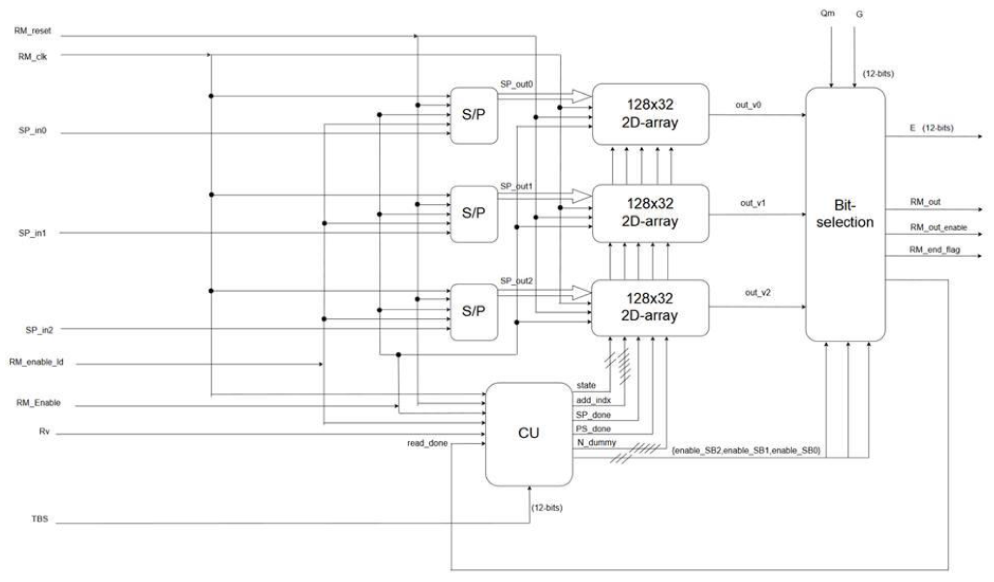
Figure 3, the design of the rate matcher block consists of the following [
10]:
The 32-bit serial-to-parallel converters, one for each stream.
One port RAMs of size bit as the maximum number of rows corresponding to TBS of 2536 bit is 81 rows.
A control unit.
Figure 3.
Rate matcher block diagram.
Figure 3.
Rate matcher block diagram.
The block’s operation starts with the write state. As the input streams are received serially and then turned into parallel to be stored in the 2D array, a 32-bit serial-to-parallel converter is used to write data row by row [
10,
11]. Afterward, the read state starts from the ninth column in the first sub-block interleaver or from the nineteenth column in the second sub-block interleaver if the redundancy version value (
) equals 0 or 2, respectively. The staring column,
, is determined according to the following equation [
14,
15]:
where
is the number of rows.
2.1.4. Channel Interleaver
This block has a crucial function, especially for the deep-fading channels where errors often occur in bursts, and consecutive bits in the same symbol may suffer from this type of burst noise. Therefore, the channel interleaver is responsible for dividing this error into a set of discrete errors and reordering bits so that the error happens in only one bit within the same symbol [
11].
The channel interleaving process is specified as a two-step procedure as follows [
10]:
This mainly depends on the number of rows and columns, as the number of columns,
, is defined as follows:
where
= 2, 4, 8, or 16 and
= 7. Moreover, the number of rows can be defined as follows:
where
G is defined as follows:
where
is the number of resource unit repetitions and has a maximum value of 10,
is the modulation indicator and has a maximum value of 2.
has a maximum combination of 24 with the number of slots,
. Thus,
G has a maximum value of 2880 and is always factorizable by 12 [
9,
10].
The channel interleaver’s block diagram is depicted in
Figure 4. To make it possible to use the RAM, bits are packed into a 12-bit long register and then stored. Furthermore, reading is carried out for 12 bits by 12 bits. The main drawbacks of using the RAM are using more logic, and one bit is read from each row (12-bit stored packet). Therefore, the number of readings is equivalent to the total number of bits. However, these drawbacks are acceptable compared to using 2880 flip-flops, which results in higher area utilization and power consumption.
The RAM memory is controlled by the finite state machine (FSM) with three states as follows:
State 0: Idle state, awaits the input’s arrival. It also works as a reset state.
State 1: Writing state, works on storing incoming bits 12 by 12.
State 2: Reading state, reads the stored bits according to the calculated number of columns and number of rows.
2.1.5. Scrambler
The scrambler block adds randomness to the data stream before applying the modulation techniques to it. Therefore, the scrambler can eliminate the long run of zeros or ones, which cause idle and reset cases. It also helps in clock recovery and having no DC component. In addition, changing the scrambling codes helps in security.
Scrambling/descrambling implementation is based on a pseudo random sequence generated from two 31-bit linear feedback shift registers (LFSRs). The two sequences of the two LFRS get XOR-ed, and the output is called a golden sequence. The sequence of the first LFSR is configured by the following polynomial [
9]:
where
is initialized as follows:
and the sequence of second LFSR is configured as follows:
where
is initialized for each codeword,
q as follows:
where
corresponds to the radio network temporary identifier (RNTI) associated with the NPUSCH transmission,
is the number of the time slot, and
is the physical layer cell identity.
Then, the two sequences get XOR-ed to have the golden sequence . Afterward, the golden sequence gets XORed with the input data. Due to the golden sequence’s initialization taking a 1600 clock cycles, it is initialized simultaneously when the subframe gets ready.
2.1.6. Modulation
This block is utilized to map the incoming bits into symbols based on the constellation of BPSK and QPSK, which are defined in [
9].
For the BPSK, each input bit is mapped to the corresponding symbol in each clock cycle, while each of the two bits is mapped to the corresponding symbol that, in turns, takes two clock cycles in the case of QPSK [
9]. A LUT is used to map the corresponding symbols.
2.1.7. Fast Fourier Transfom (FFT)
The modulated symbols pass through the fast Fourier transform (FFT) block, which performs the single-carrier frequency-division multiple access (SC-FDMA) modulation technique to reduce the peak to average power ratio (PAPR), which correspondingly reduces the power consumption [
16]. The FFT block has to support the different values of the number of subcarriers, which can be 1, 3, 6, or 12 subcarriers, as stated in [
9].
To cope with the continuous stream of QPSK or BPSK modulated symbols, the choice of a pipelined implementation is necessary to avoid buffering before the FFT block, which can cost a lot in leakage power and area [
17,
18,
19]. In addition, with the continuous stream at the input, the FFT unit also has to calculate the different points (3, 6, 12), which necessitates that the pipeline shares resources efficiently.
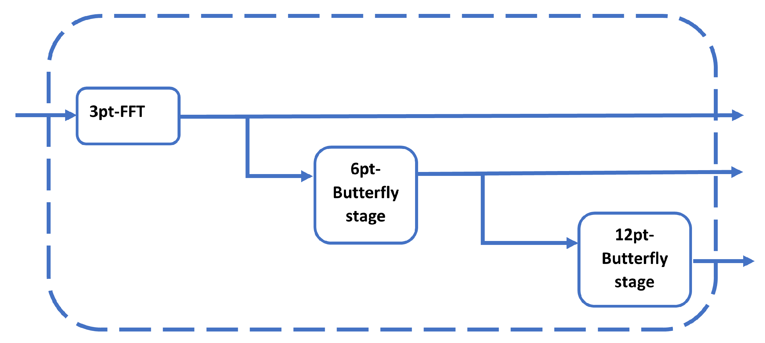
The algorithm is mainly based on two ideas: the first one is to reuse a single 3-point FFT pipeline in calculating the 6- and 12-point FFTs, and to reuse the 6-point FFT butterfly stage pipeline to calculate the 12-point FFT as is illustrated in
Figure 5. This can be possible by initially reordering the input samples. The second idea is to increase the time utilization of the 3-point FFT pipeline by freezing the inputs for 3 clock cycles so that all inputs are available, and hence the calculations can be serialized without adding delay. This results in a hardware reduction by half.
2.1.8. Narrowband Demodulation Reference Signal (NDMRS)
In NB-IoT Uplink channel, NDMRS are used as pilots for channel estimation in the receiver chain. The channel estimation block’s main function is to estimate the changes that occur in the data bits while they go through the channel so that the change can be reversed and the data can be corrected. This channel correction is performed by sending pilots—NDMRS—with the data bits which will be affected also by the channel, and the receiver generates these pilots using upper layer parameters. Following that, if the received pilots are divided by the generated ones, this creates the channel effectwhich will be delivered to the equalizer to reverse it [
10].
2.1.9. Resource Element Mapper (REM)
The REM’s function is to assign the FFT symbols to the proper subcarriers at the IFFT block’s input. As in the case of 12-point FFT, all FFT symbols are allocated to the 12 subcarriers. Whereas, in the case of 6-point FFT, the output 6 symbols of the FFT are assigned to specific 6 subcarriers out of the 12 subcarriers, and the remainder is zero-padded; the same is conducted for the 3-point FFT case. The symbols’ location within the 12 subcarriers is calculated according to information from the upper layer in the case of 3 and 6 subcarriers [
9,
10,
12].
2.1.10. Inverse Fast Fourier Transform (IFFT)
IFFT block is responsible for transforming the frequency subchannels into the time domain samples to be transmitted through the radio frequency (RF) blocks. It is challenging for the IFFT block to be at the end of the transmitting chain, as it must satisfy the required output rate (i.e., new SC-FDMA symbol in each SC-FDMA symbol duration) and not only generate this symbol within this duration, but also with a fixed rate [
12].
The IFFT subcarriers are packed into groups of 12 subcarriers with 15 kHz spacing between each adjacent subcarrier; each group is recognized as a resource block, and the NB-IoT has only one resource block per the UE transmitter. To implement the IFFT block, which supports 12 subcarriers (the maximum number of allocated subcarriers), a 16-point IFFT is used due to its minimum area utilization in order to decrease the power consumption and the latency of the block. In addition, the reduced output sample rate of this block is compensated using an upsample filter to improve the rate to a proper rate for the digital-to-analog converter (DAC) block [
12].
The design of the IFFT block consists of 4 stages, each consisting of butterflies. The first stage needs one butterfly, the second needs two butterflies, the third needs four butterflies, and the last one requires eight butterflies as shown in
Figure 6.
2.1.11. Interpolation
This block aims to upsample the IFFT output, add a certain number of samples at the starting of each symbol, known as cyclic prefix (CP), to remove the intercarrier interference (ICI) and the intersymbol interference (ISI), and convert the symbols from parallel to serial flow of samples [
9]. The interpolation procedure varies with the frequency spacing,
as follows:
When kHz, the upsampling becomes 8 times to convert the 16 samples to 128 samples with 10 samples for the CP of the first symbol in the time slot, and 9 samples for the CP of the other 6 symbols in the same slot.
When kHz, the upsampling becomes 32 times to convert the 16 samples to 512 samples with 40 samples for the CP of the first symbol in the time slot, and 36 samples for the CP of the other 6 symbols in the same slot.
2.2. NPDSCH Receiver Chain Implementation
2.2.1. Coarse Synchronization
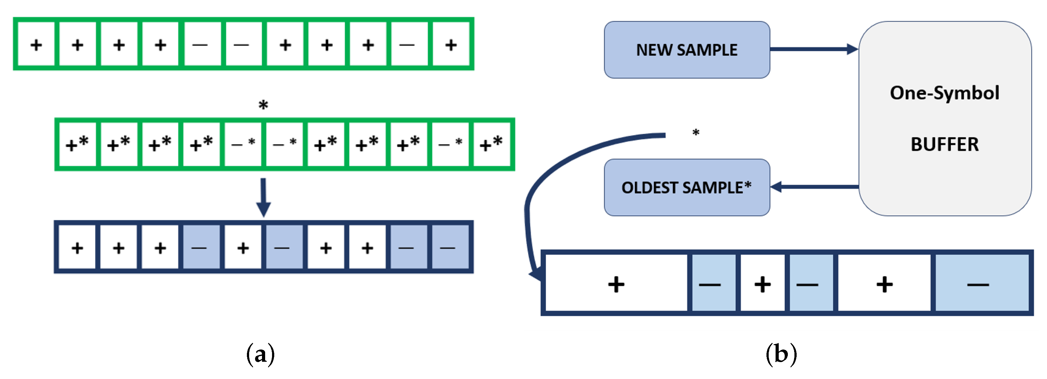
The synchronization process is performed in both time and frequency by using the narrowband physical synchronization signal (NPSS). The first step of the synchronization procedure is coarse synchronization, which has simple computations and reduces the complexity of its following step, refined synchronization [
5]. The coarse synchronization block makes use of the NPSS periodicity and the good correlation properties to estimate the time and frequency offsets with reasonable accuracy, frequency offset 50 Hz accuracy, and time offset 2 samples accuracy, performs CP removal and down-sampling after the synchronization process is terminated, and provides information about the symbol’s position to facilitate the remaining chain’s operations or serve the high layer requests.
The synchronization procedure introduced in [
20] is implemented in this work using the metric of reduction and normalization method presented in [
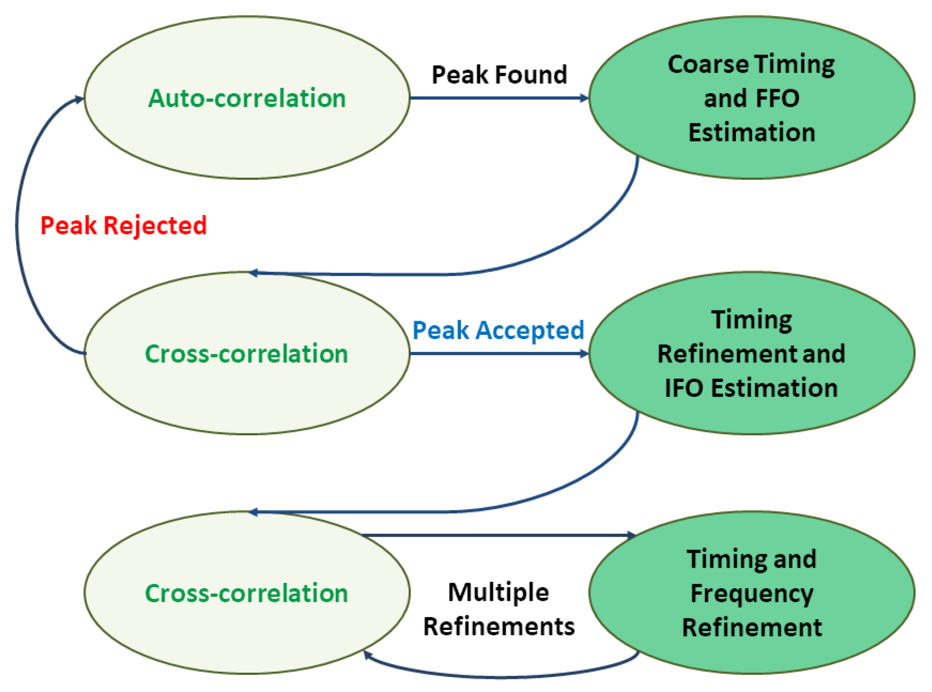
21]. This implementation provides good performance at the minimum SNRs, in terms of speed and residual time and frequency errors, which are all investigated using an experimental FPGA-based hardware implementation method. As illustrated in
Figure 7, the synchronization procedure consists of three steps, where the green color for the timing stages and the off-white color for the correlation (auto or cross) stages. The first step is to use a reduced averaged time domain auto-correlation metric to acquire a coarse timing by detecting the NPSS and a fractional frequency offset (FFO) estimate, leveraging the repetitive nature of the NPSS. This auto-correlation metric originally has one frame of 19,200 samples length, but it is reduced by a factor of 16 to decrease the memory requirements. Since the detection process has low resolution at low SNRs, it is averaged over frames to reduce the impact of the additive white Gaussian noise (AWGN). The metric is stored and when the maximum exceeds a certain threshold; it is considered a possible solution, and it is tested throughout the following procedure’s step. The second step is to refine the timing estimate and to estimate the integer frequency offset (IFO) using a time domain cross-correlation metric. The auto-correlation peak is considered false if the maximum does not overtake another certain threshold and therefore the procedure goes back to the first step. Otherwise, it continues to step three. The third and last step implements the same metric of the second step multiple times on a local time–frequency grid to refine the timing and frequency estimates [
20].
The data flow through the states can be defined as follows:
The time domain samples are stored in a buffer that has the size of one NPSS symbol to implement the lag and the multiplication operation in (
18); hence each input sample will be multiplied with the conjugate of the oldest sample stored in the buffer.
where
is the auto-correlation metric calculated in a single frame for a sample with index,
19,199, and
represent the auto-correlation window and are equal to 1370, which is the length of 10 symbols and each has the length of
samples.
r is the received signal given by (
19), and
S refers to the code cover defined in [
9,
20].
where
is the transmitted baseband OFDM signal,
is the impulse response of the multipath channel, and
represents the AWGN.
represents the frequency offset normalized to the subcarrier spacing and it has two components: the integer frequency offset,
and the fractional frequency offset,
.
The resulting products will be stored in buffers that have, in total, the length of the auto-correlation window, but the separation is sign based. The aim is to keep all the products that have the same sign—resulting from the code cover—together in buffers so that each buffer contains products that have the same sign. As the operation progresses, new products will push old products down into the buffers chain, and accordingly, their sign will change at the transitions. This technique is complemented by creating an accumulator to each buffer to add all the incoming products minus the outgoing products. Thus, at each moment, these accumulators will contain the summations of their buffers and by adding them according to the sign pattern, the total summation of (
18) can be defined.
Figure 8 depicts this state.
At each arriving sample, the buffers will be added accordingly, and the result of these additions will be reduced in number by adding them, then the resulting value will be a metric entry, as it will be added through the normalization filter as mentioned in (
20) and (
21). These values will be stored, and the maximum will be compared to the threshold until a peak is found. This will conclude the states of the buffers filling and the NPSS search.
where
is the reduced metric for one frame and
is the final form of the metric as the values accumulated through previous frames are updated with new values using the normalization filter that has the factor
.
The last two steps in the procedure begin with loading compressed NPSS samples into a complete symbol to be used in the cross-correlation calculations. The operation will be implemented by alternating between the states “IFO and Refinement Calculations” and “Cross-Corr”, as the first state captures all time hypotheses’ samples, and sorts last iterations metric whereas, the second state performs the cross-calculation itself by using CORDIC phase rotators fed by phase accumulators to perform the calculation for all frequency hypotheses at a certain time hypothesis. Following that, the result is stored and compared to the threshold. To sum it up, the decision making and sample capturing are performed in the state “IFO and Refinement Calculations”, and the actual calculation is done in the state “Cross-Corr”.
In step two, if the cross-correlation maximum passes the threshold, the state machine will proceed as mentioned above through step three and into normal operation in the state “Locked”, and if not, the state machine will return to the first state through an intermediate reset the state “False Peak State”.
2.2.2. Carrier Frequency Offset (CFO)
The functionality of the CFO block is to cancel the frequency offset that introduces the ICI and impacts the orthogonality of subcarrier. The frequency offset occurs due to the following:
It is divided into two types; the integer carrier frequency offset,
that comes from the coarse synchronization block, and the fractional carrier frequency offset
that comes from the fine synchronization block. The received signal can be defined as follows:
The
is the modulated data,
N is the number of subcarrier used,
is the channel gain at
kth subcarrier,
is the AWGN noise, and
is the frequency offset, which is determined in (
23) as
The effect of the offset on the received symbol can be canceled by multiplying (
22) by the exponential raised to the phase conjugate to the estimated offset as follows:
where
is the corrected symbol. As a complex exponential represents rotation of
, the CORDIC design is utilized with its rotation mode [
22], and the phase accumulator is used to accumulate the offset each cycle. In the CORDIC implementation, 15 stages and the recursive pipelined design are implemented. Moreover, that design has lower area and consumes lower power than that in [
23,
24].
2.2.3. Fast Fourier Transform (FFT)
The Cooley–Tukey algorithm is considered a breakthrough in implementing fast Fourier transform (FFT), which reduces the DFT complexity. The DFT of a signal in the time domain
is introduced as follows:
The is known as the twiddle, which is a complex value. In order to compute the N point of the DFT, it is required to perform operations; however, by using the FFT, the required operations are down to .
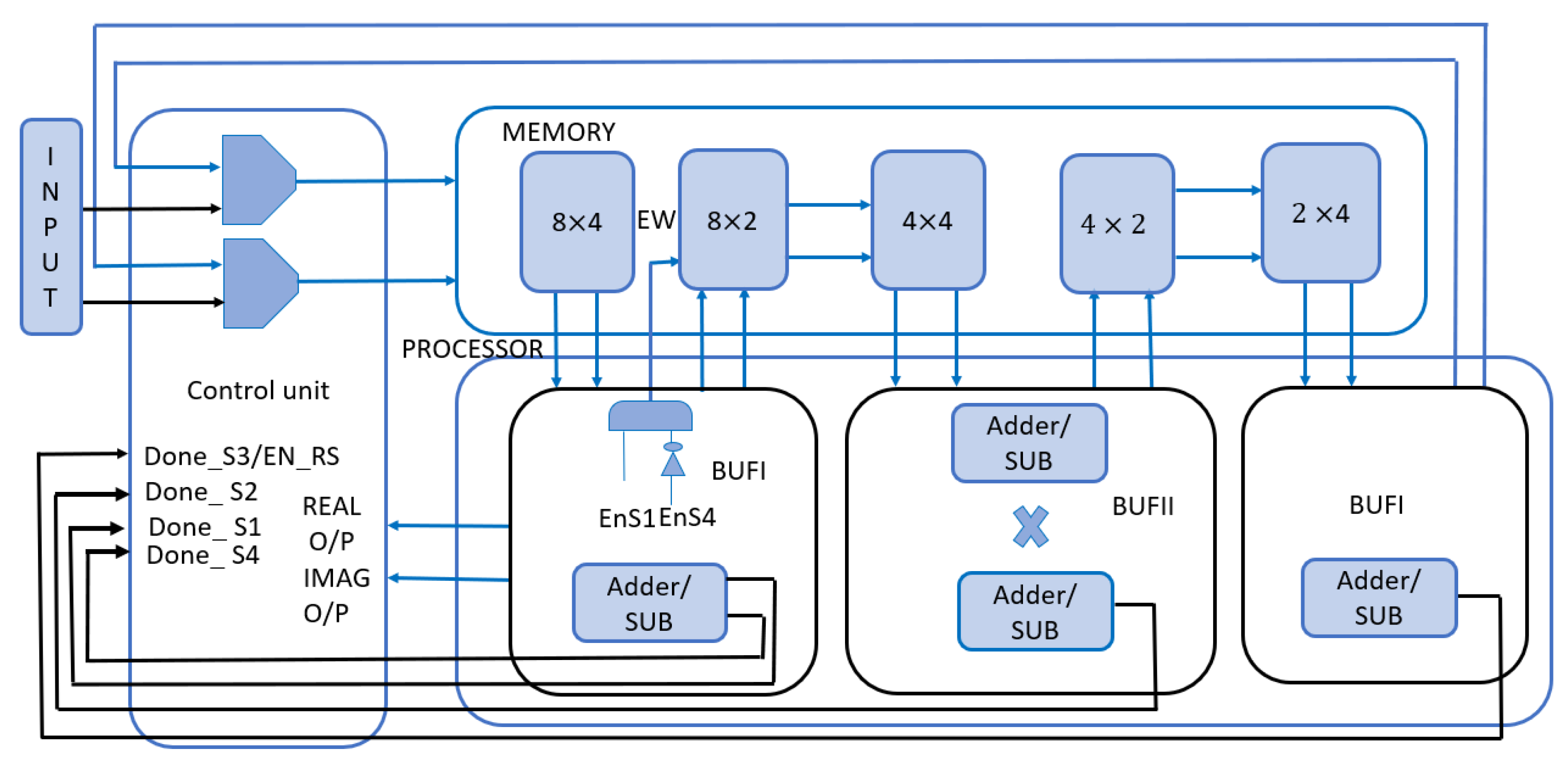
The implemented algorithm is 16-point FFT using Radix
single-pass delay feedback (SDF) algorithm, which is the best fit for the limited NB-IoT power budget. The SDF is implemented with parallelization
to reduce the power consumption and the area of the design. It also helps in enhancing the block latency and performance [
25]. Radix
has been developed to inherit the simple control structure of radix 2, and it has the advantage of saving hardware, i.e., reducing the number of used multipliers in contrast with radix 4 [
26,
27].
The output of the CFO block passes first through a synchronous first in first out (FIFO), then enters the FFT block. As depicted in
Figure 9, the block mainly consists of memory and a butterfly, where the butterfly’s output is stored in the 3D memory. Therefore, it is stored in the same row, which helps in power optimization as there is no need to use an address generated circuit. Moreover, as the pipeline is deployed, there is no need to have a large memory like the memory-based algorithm. That improves the design performance and reduces the leakage power and the switching activity. At last, the 16-point FFT requires the data to pass through four stages to complete their operation, but only three stages are implemented, as the fourth stage is shared with the first stage to reduce the consumed resources and the power consumption. In addition, the bit reversal operation for the FFT output symbols is performed while storing in the storage element before entering to the resource de-mapper.
2.2.4. Resource Element De-Mapper
The PRB consists of
consecutive OFDM symbols in the time domain and
consecutive subcarriers in the frequency domain, as it comprises
resource elements (REs), corresponding to one time slot and 180 kHz in the frequency domain. PRBs are numbered from 0 to
in the frequency domain [
28,
29]. Resource block pair consists of two resource blocks: the even numbered frame and the odd numbered frame. As in NB-IoT, the normal CP is used, where
kHz,
, and
. Therefore, the subframe is
, and only one antenna port is used. Then the NB-IoT carrier uses one LTE PRB in the frequency domain where there are 12 subcarriers of 15 kHz for a total bandwidth of 180 kHz [
28,
29].
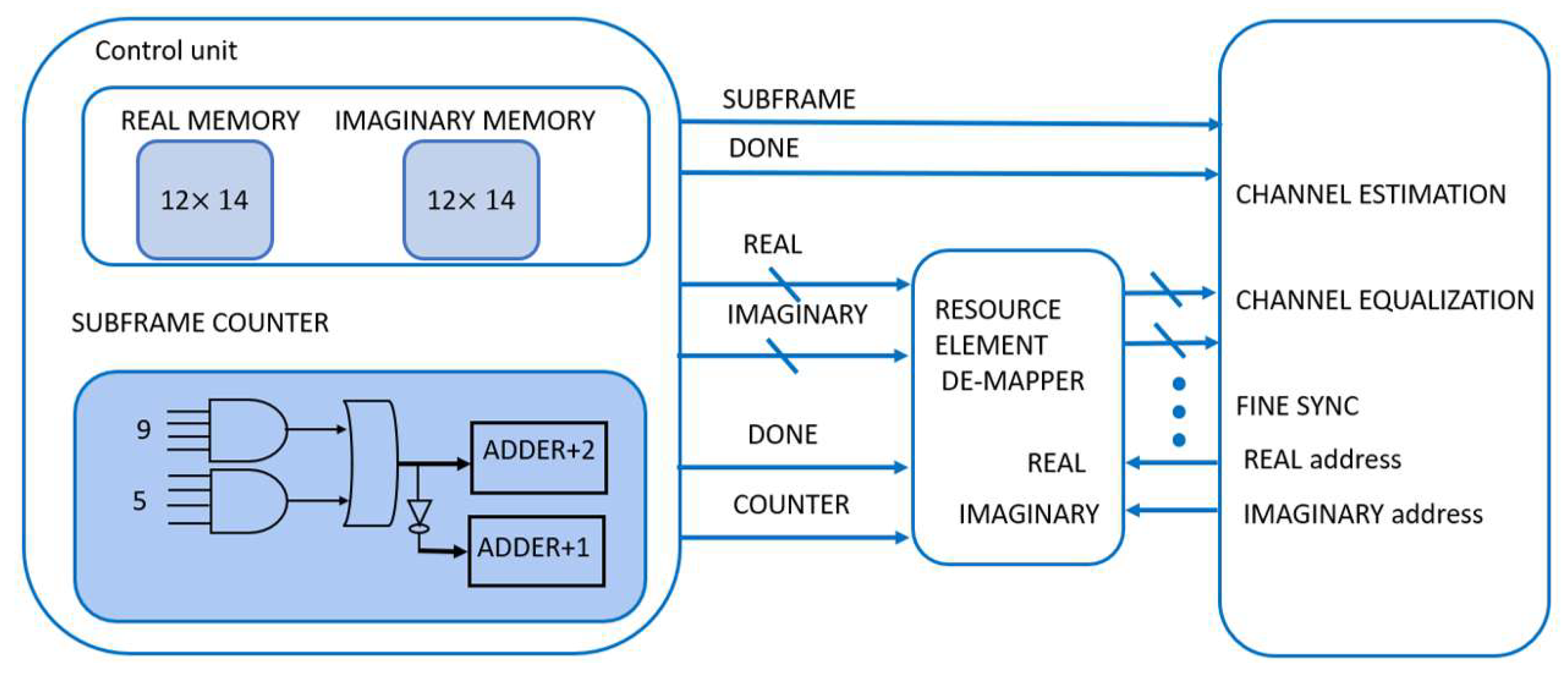
As shown in
Figure 10, the resource de-mapper takes the output of the FFT and then the output is stored in its memory to be used by the channel estimation, channel equalization, and fine synchronization using the row and column address. The block includes a
storage element memory, which stores the unsorted FFT output, and when it is full, an enable signal is raised to let the resource de-mapper get the symbols column by column. Correspondingly, it takes 14 clock cycles to fill the resource de-mapper. Thus, the time in which the resource de-mapper is kept unchanged is approximately 1 ms as stated in the 3GPP standard [
9].
In the storage element memory, the bit-reversing of the FFT output takes place, and the symbols stored in this memory are in-order. Then, when transferring the data from storage element memory to resource element de-mapper the symbols are resorted as the last six symbols stored in first six symbols and the first six symbols are stored in last six places in memory.
2.2.5. Channel Estimation
The channel estimation process attempts to define the effect of the channel on transmitted signals. In NPDSCH, the pilot-based channel estimation is used by generating some symbols, known as pilots at the transmitter and generating the same symbols at the receiver to find the relation between the received and original symbols and get a rough estimation of the channel. These pilots are carried by the narrowband reference signal (NRS), which exists in all the subframes transmitted, except the NPSS subframes and the narrowband secondary synchronization signal (NSSS) subframes [
5]. The values of the NRS pilots are calculated as follows [
9]:
where
l defines the number of NRS symbols, as it can be 5 or 6 symbols.
is the time slot number, taking values from 0 to 9.
m equals 0, 1,…,
as the
so,
m is just equal to 0 or 1. Moreover,
c refers to pseudo-random sequence generation defined by a length-31 gold sequence as follows:
The first m-sequence has a constant initialization as follows:
while the second m-sequence is based on the application. Therefore, the NRS generation
has the following initialization,
:
where
is an input,
is the time slot number,
equals 1600 clock cycles, and
for the normal CP.
Moreover, the locations of the NRS symbols can be determined as follows [
9]:
where
k refers to the place of a pilot to be in which row, ranged from 0 to 11, as the row refers to the subcarrier and the variables, and
v and
define the position in the frequency domain for the reference signal as
is equal to
.
There are many channel estimation algorithms used in NB-IoT receiver but there is a trade-off between the complexity of the design and its performance. Accordingly, the least square (LS) channel estimation algorithm [
30] is selected to be adopted in the implemented chain, and to compensate the performance, the interpolation process is deployed to obtain better performance with low complexity. The used interpolation is linear interpolation, which is calculated every subframe, as the channel estimation gets 12 different outputs,
, and each is used by the equalizer with one of the 12 subcarriers [
31]. Furthermore, the extended typical urban (ETU) model is deployed according to the 3GPP standard [
32]. The specification for the channel model used in simulation is a Rayleigh fading channel with an extended typical urban delay profile, maximum Doppler frequency shift equal to 5 Hz, and a sampling frequency equal to 1.92 MHz.
Let the signal at the receiver after the channel effect be
y, as
. Here,
x is the transmitted signal,
H is the channel frequency response, and
n is the AWGN. Then, the least square channel estimation algorithm is
, as the channel estimation block aims to divide the received pilots over the transmitted pilots to get the channel effect on the transmitted symbols [
30].
Figure 11 depicts the block diagram of the channel estimation block. The transmitted/generated pilots are extracted out of the NRS generator and the received pilots are determined from the resource mapper. Then, the channel frequency response is calculated, and the four channel frequency responses obtained from the eight pilots are stored. At last, interpolation is performed to get the 12 channel frequency responses for the equalizer.
2.2.6. Channel Equalizer
After estimating the channel effect, the equalizer plays its role to cancel the intersymbol interference (ISI) and the noise by divided the channel effect over all the transmitted symbols as follows [
9]:
where
is the equalized symbol,
is the received symbol,
represents the channel,
is the estimated value of the channel, and
is the AWGN value.
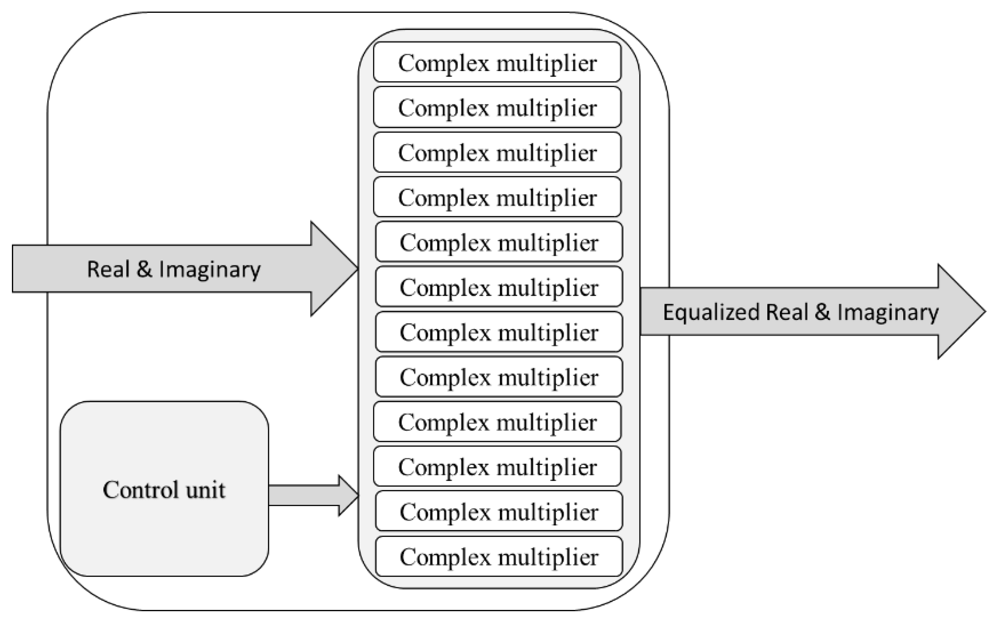
The block diagram of the channel equalizer block is shown in
Figure 12. The main sub-block of the equalizer block is the complex divider but instead, the complex multiplier can be used to reduce the area utilization and the power consumption.
2.2.7. Parallel to Serial and NRS Removal
In this block, the inputs should be applied serially starting from the modulation block to the CRC block. Additionally, the NRS symbols need to be removed from the equalizer’s output, as the data at the transmitter do not contain them.
2.2.8. Symbol De-Mapper and Demodulation
In the demodulation process, the received symbols are mapped to values of ‘0’ or ‘1’ based on the constellation tables. The techniques used in demodulation are hard decision and soft decision, which both use log likelihood ratio (LLR). The soft decision technique gives less bit error rate (BER) than that of the hard decision technique, but due to using QPSK modulation, which gives small BER compared to, for example, 16 QAM, the hard decision technique is used [
9,
23].
The symbol de-mapper block takes the most significant bit (MSB) of each bus
that comes from the NRS removal block, then the symbol is de-mapped based on its sign. The inputs of this block are two buses; each sends 12 serial bits and it also works with the double rate of the NRS removal block [
9].
2.2.9. De-Scrambler
The de-scrambler block has the same working operation of the scrambler block discussed earlier in the NPUSCH transmitter chain. The resource de-mapper provides the frame and subframe numbers and when the resource de-mapper completes its function and raises its done signal, the De-scrambling starts to work. After initialization, the de-scrambler sends a ready signal to the channel equalizer block. Additionally, the output of de-mapper, which is 24 serial bits is the gold sequence’s code word length, and the rate of the de-scrambler is equal to the de-modulation rate. The de-scrambler measures the length of the time slot in the resource de-mapper. If it equals 10 symbols, it stops and stores the remaining code for the next slot, as the NRS signals are not descrambled [
9].
2.2.10. Rate De-Matcher
The function of this block is to reverse the rate matching process. The output of the rate de-matcher block is three original data streams that are generated from the tail biting convolutional encoder in the transmitter [
33].
As illustrated in
Figure 13, the rate de-matcher mainly consists of a bit collection sub-block and de-interleaver sub-blocks. The bit collection sub-block includes a memory with size of
×
, which will be (
). The size of this memory is large because in this release, the maximum TBS is 2536 bits [
32]. The input to this sub-block is the data stream of the circular buffer in the transmitter with any length according to the upper layer set parameter. The de-interleaver sub-block consists of four memories; each has a size of the number of columns multiplied by the number of rows for the maximum TBS, which equals
[
34]. This sub-block should comprise three memories to store the whole data stream, but here, there are four memories, as the fourth memory is used for the consecutive input stream.
2.2.11. Channel Decoder
Forward error correction (FEC) is one of the techniques applied to detect and correct errors in the received data without the need for retransmissions. The convolution encoding with Viterbi decoding is considered a powerful method for the FEC, where the data are convoluted and then transmitted into a noisy channel. This process involves an insertion of redundant data, which helps in detecting and correcting errors due to those noisy channels. The Viterbi algorithm is the most powerful method for decoding the convoluted data in terms of bit error rates and efficiency, as it tracks down the most likely sequences that the encoder has gone through, and uses this information to deduce the original message [
35].
A (
) convolutional encoder has
m stages,
k bits entering the shift register at each time instant and
n output bits, which are formed using the following generator sequences [
10]:
The encoder rate R is equal to .
The Viterbi decoder applies a tree search procedure to optimally detect the received data sequence. It calculates a measure of similarity between the received signal, entering each state at time and all the trellis paths, and removes all candidates that are not possible based on the maximum likelihood (ML) choice. Each received sequence goes through a number of computations starting with branch metric computation, where the Hamming distance is calculated and is then followed by path metric computation, where errors are accumulated and stored to be used in the decision making. At the end of the received sequence, a trace back procedure starts from the path with the least number of errors [
35].
The decoding of the convolutional codes is done by applying the modified circular Viterbi algorithm, which performs several iterations of the Viterbi algorithm until a tail biting pattern is found. The decoding steps can be listed as follows [
35]:
Start the Viterbi algorithm with initial metrics set to zero.
Compute the survival path based on the path with the least accumulated metric.
If this path is a tail biting path, decoding stops and the survival path is decoded.
If the survival path is not a tail biting path, metrics are updated with final metrics of the previous iteration.
Apply the Viterbi algorithm on the same message, until a new survivor path is obtained.
If the new survivor path is a tail biting path, the algorithms stops.
If maximum number of iterations is reached, the algorithm stops, and the best survival path is decoded.
The decoded sequence is stored in a last in first out (LIFO) memory to be passed in order after the tail biting condition is checked correctly.
2.2.12. CRC
The CRC block in the NPDSCH receiver uses the same technique as the transmitter, and if the remainder is zero, that means the data are correct; otherwise, the data are incorrect. The CRC block receives the data from the viterbi decoder and passes them to the upper layer [
10].
2.2.13. RAM Memory Resources Sharing
Due to the large similarly-sized memory requirements in the synchronization block and the rate de-matcher block and the fact that the two blocks do not simultaneously access their memories, it becomes appealing to share the RAM resources of these blocks. Mainly, the sharing is made possible by multiplexing the two clocks of the blocks with the selection of the LOCKED signal which indicates the activity of the synchronization process. This signal is also used to multiplex the inputs to the RAM, the pointers, and the enables. Additionally, a multiplexing process is implemented to help implement the rate de-matcher RAM as multiple smaller RAM blocks.
3. System Integration
In this section, the integration with MATLAB and RTL and the synthesis results are presented. The experimental implementation using FPGA is highlighted as well.
3.1. MATLAB Integration
After modeling the chain’s blocks using MATLAB, a NPDSCH transmitter is designed using MATLAB built-in functions based on 3GPP standard Rel-14. Then, the channel model ETU is added with a maximum Doppler shift of 5 Hz, 9 taps, and a maximum excess tap delay of 5 μs [
32]. A noise model using AWGN is applied with the minimum required SNR for the design, −12.6 dB [
20]. Finally, frequency and time offsets are applied, where the range of frequency offset is [−35:35] kHz and time offset range is [0:192,000] samples [
20]. In addition, the receiver’s chain is added in a generic format to satisfy all TBSs and repetition ranges. The system is tested for repetitions of 1, 32, 64, 128, 256, 512, and 1024 under SNR ranges [−14:20] dB. The designed model is compared with the reference model by MathWorks [
36] as shown in
Figure 14 [
36]. The two models are not completely identical, as the MathWorks model uses the following:
A perfect synchronization.
A perfect frequency correction using exponential, but cordic in the presented model.
A perfect channel estimation.
A soft symbol de-mapper.
A soft decoding.
Figure 14.
BLER vs. SNRfor MATLAB and RTL designed model compared with ideal model.
Figure 14.
BLER vs. SNRfor MATLAB and RTL designed model compared with ideal model.
3.2. RTL Integration
In the specification phase, the signal interface for each block and the output rate from each block are defined that helps in the chain integration. MATLAB is used to generate a text file, which the test bench reads a symbol per clock cycle from. The RTL system is tested with the same way used in MATLAB as a python script is used to run MATLAB, generating the files, then ModelSIM is run to simulate the design. Finally, MATLAB is run again to calculate the BER and the BLER that are illustrated in
Figure 15.
3.3. Synthesis Results
The whole design is synthesized using Xilinix Vivado 28 nm. The Vivado utilization of the whole chain implemented on Virtex 7 is depicted in
Table 1.
3.4. FPGA Implementation
The generated files from MATLAB are stored into a read only memory (ROM), and the interface of the chain to the ROM is created. By using the debugging tools in VIVADO, virtual input output (VIO), and integrated logic analyzer (ILA), the output should be observed from the chain to make sure that the results are correct. Additionally, the mixed-mode clock manager (MCMM) in FPGA is used to generate deferent clock domains to make sure that the phases between them do not change as time passes.
4. System Architecture
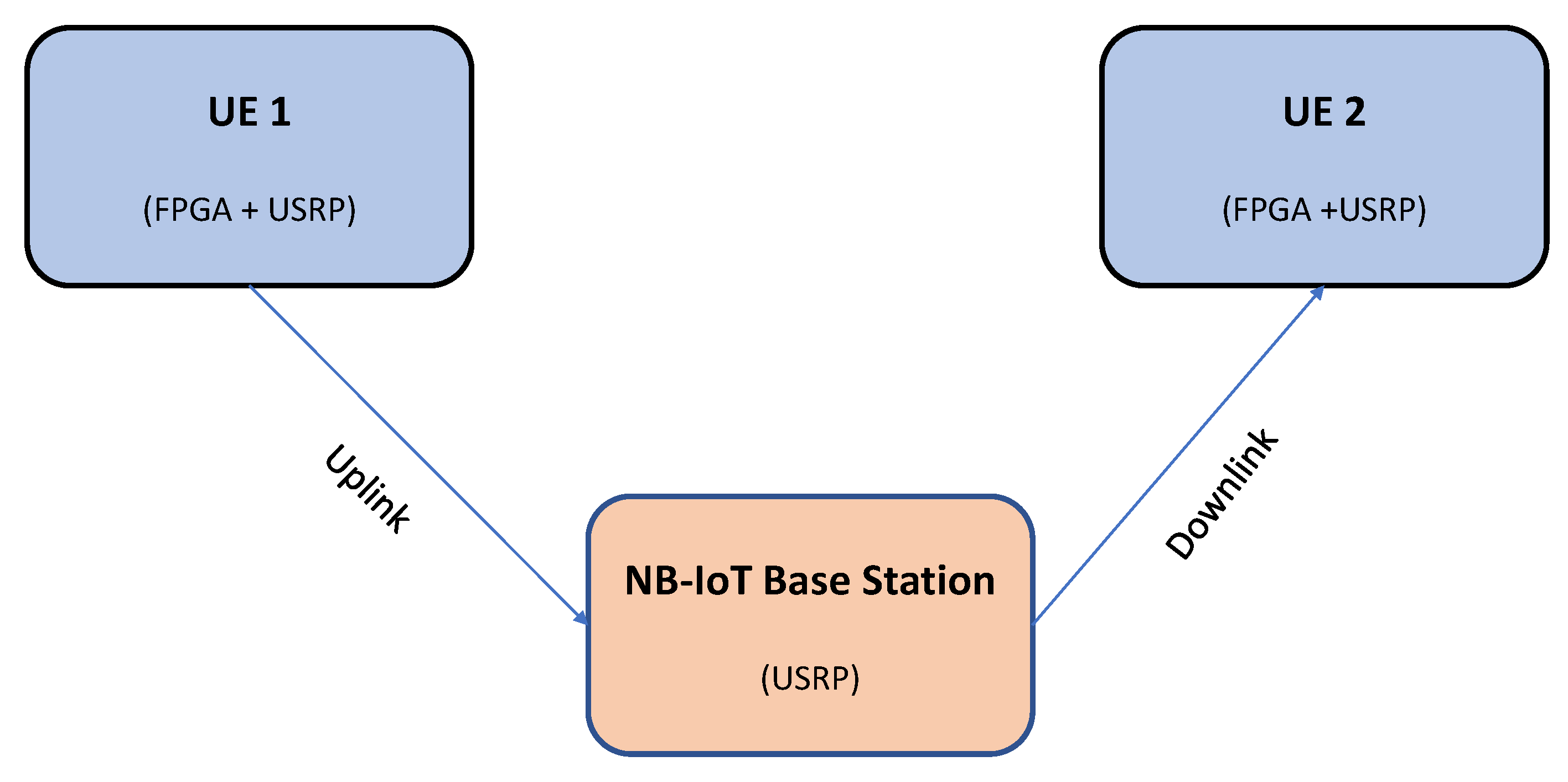
As illustrated in
Figure 16, the implemented NB-IoT system consists of two user equipment (UE1 and UE2) and the NB-IoT base station. The UE1 implements the NB-IoT transmitting chain to transmit its data to the base station, which in turn sends these data to the UE2. The UE2 implements the NB-IoT receiving block chain to receive the data from the implemented base station.
Two field programmable gate arrays (FPGAs) and two NI universal software radio peripherals (USRPs) are used for both UEs. In addition, another NI USRP is deployed as the base station. For the software part, MATLAB is used to build the NB-IoT base station as well as the NB-IoT transmitting and receiving chains that are converted to RTL to implement them on the FPGAs. Additionally, GNU radio is used to interface with the USRPs, which act as the system’s radio frequency (RF) front end.
The connection between FPGA and the USRP in the UE1 can be illustrated as follows. The NB-IoT transmitting chain is implemented on the FPGA, which sends the generated orthogonal frequency-division multiplexing (OFDM) symbols to the USRP. Therefore, the USRP starts to transmit the symbols towards the base station.
4.1. The Universal Software Radio Peripheral (USRP)
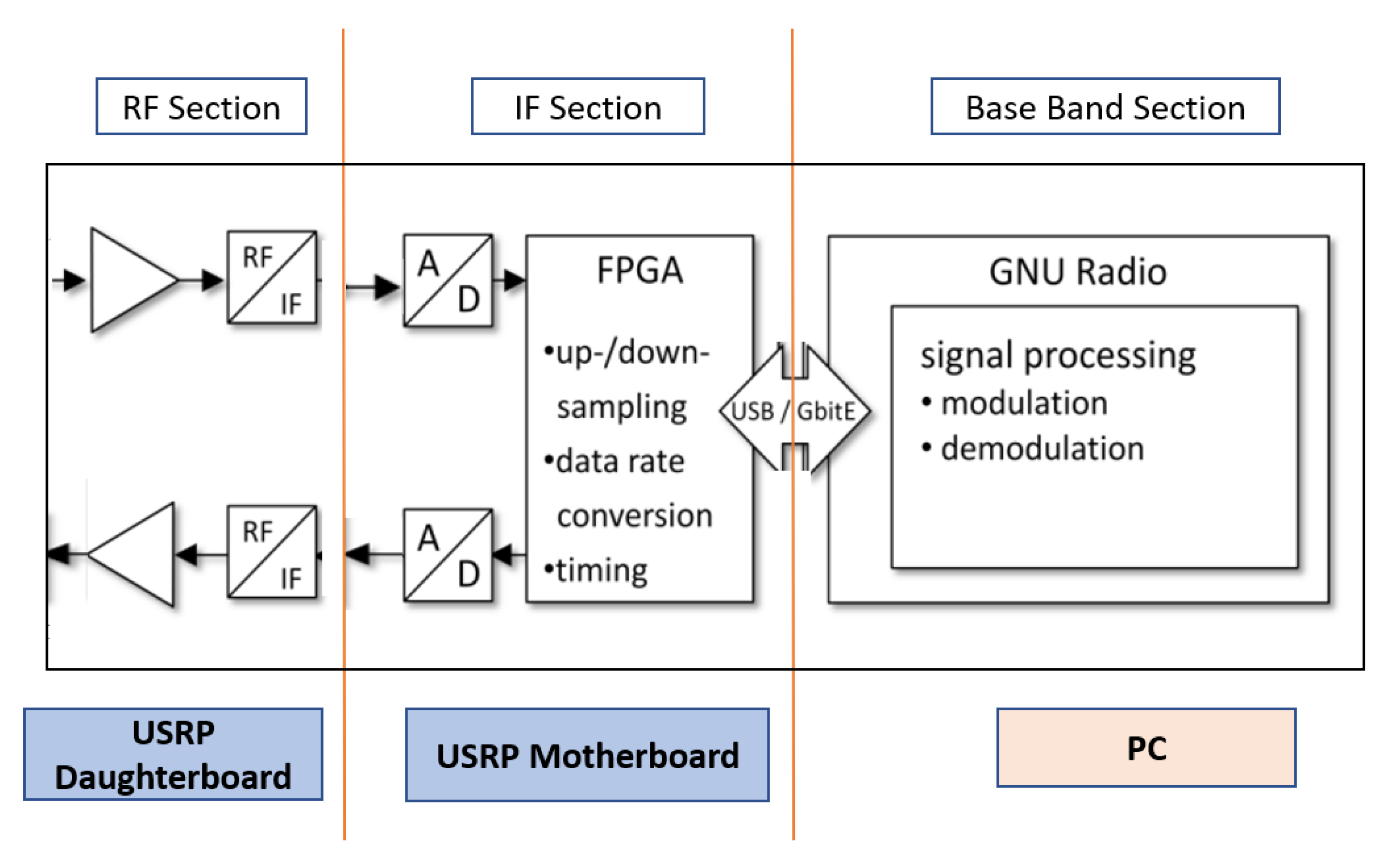
The USRP consists of three basic functional blocks: the baseband section, the IF section, and the RF section, as shown in
Figure 17. The RF section contains the RF circuit (USRP’s Daughterboard) responsible for transmitting and receiving the RF signal at the operating frequency. The IF section (the USRP motherboard) contains the processing FPGA that performs the signal processing, such as filtering, modulation, and demodulation. Additionaly, it contains the analog-to-digital converter (ADC) and the digital-to-analog converter (DAC).
In this work, NI USRP B200 is used, which has the following features:
It is the first fully integrated USRP that covers RF range from 70 MHz to 6 GHz.
It uses SuperSpeed USB 3.0.
It covers up to 56 MHz of instantaneous bandwidth.
It is a full duplex device and SISO (1 TX and 1 RX).
4.2. The Field Programmable Gate Array (FPGA)
By using the debugging tools in VIVADO, virtual input output (VIO) and integrated logic analyzer (ILA), the inputs and the outputs should be observed from the chain to make sure that the results are correct. Additionally, the MCMM in FPGA is used to generate deferent clock domains to make sure that the phases between them do not change as time passes.
From the UL view, the generated files from MATLAB are programmed into a RAM and make the interface of the chain to the RAM. The data are transmitted by the USRP after receiving from the UL and then the DL is started with the same method. At last, it is possible to check the BER on FPGA by comparing the received data with the transmitted data.
5. NB-IoT System Implementation
In this section, the implemented GNU radio companion (GRC) flowgraphs are illustrated for the transmitting/receiving uplink, the transmitting/receiving downlink, and the whole system’s hardware set-up.
5.1. The Transmitting Uplink
The flowgraph shown in
Figure 18 is implemented to send the OFDM symbols file from the UE1 toward the base station using the USRP. The flowgraph consists of the following blocks:
File Source: It is the head of the flowgraph and contains the transmitted symbols file.
Packet Encoder: It packetizes the transmitted bytes into frames and has two necessary parameters (samples/symbol and bits/symbol).
GMSK Mod: it is responsible for the GMSK modulation process with the same value of the samples/symbol parameter of the packet encoder block and has a filtering degree of .
Multiply Constant: It multiplies the input stream by a scalar or a vector constant to control SNR.
UHD: USRP Sink: It is the block for combining with the USRP and sends the stream to it to start transmitting it.
Figure 18.
GRC flowgraph of the transmitting uplink.
Figure 18.
GRC flowgraph of the transmitting uplink.
5.2. The Receiving Uplink
To receive the transmitted symbols on the base station, the flowgraph shown in
Figure 19 is designed, and that is certainly the reversed flow of the transmitting uplink flowgraph starting with the block of UHD: USRP Source, which is responsible for combining with the USRP and makes it ready for the reception and passing through a low pass filter, GMSK demodulation, and packet decoding. The block of WX GUI FFT Sink is used to ensure that the USRP does receive the data, as this block generates an FFT plot that gives a peak with the USRP reception. The flow ends with the File Sink block, in which the location of the received data are defined.
5.3. The Transmitting Downlink
After receiving the symbols on the base station’s USRP, the MATLAB base station is run and, alternately, has two files of the real and the imaginary parts of the symbols, which are sent separately to the base station’s USRP to start to transmit them toward the UE2.
In
Figure 20, two flowgraphs on GNU radio are illustrated of this part, as one is enabled at a time, and they are the same flow of the transmitting uplink part, only changing the file added to the file source block to the generated files from the base station MATLAB code.
5.4. The Receiving Downlink
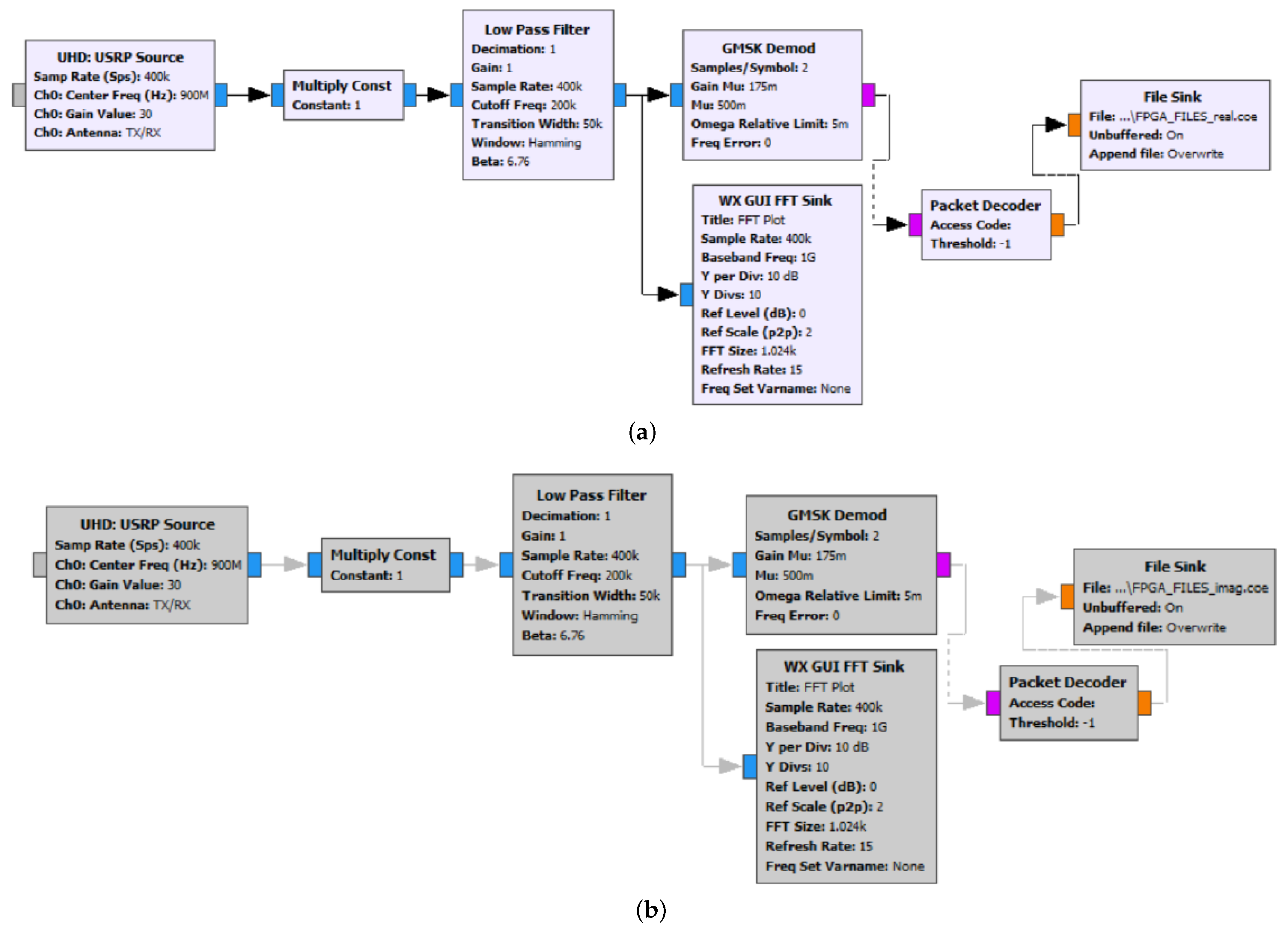
In this part, the data transmitted from the UE1 to the UE2 through the base station are received correctly using the flowgraph shown in
Figure 21. These two flows are the same as those of the receiving uplink part.
5.5. Hardware Set-Up
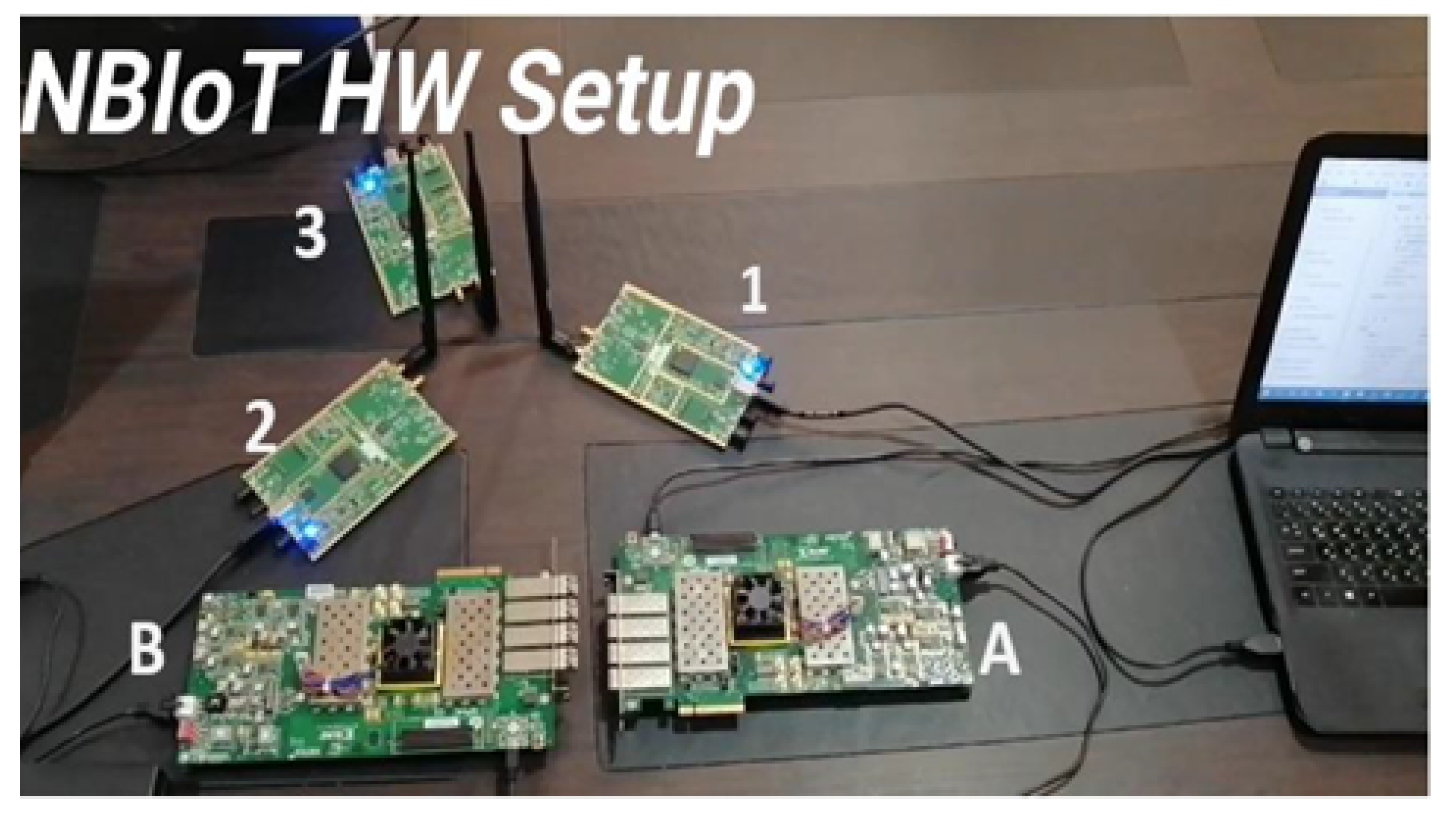
Here, the whole system setup is presented; as mentioned before, three USRPs are utilized working at a frequency of 900 MHz and a gain of 30 dB and two FPGAs. As shown in
Figure 22, the two FPGAs and the three USRPs are ready for transmission and reception. The parameters of NB-IoT hardware setup components are described in
Table 2.
As illustrated in
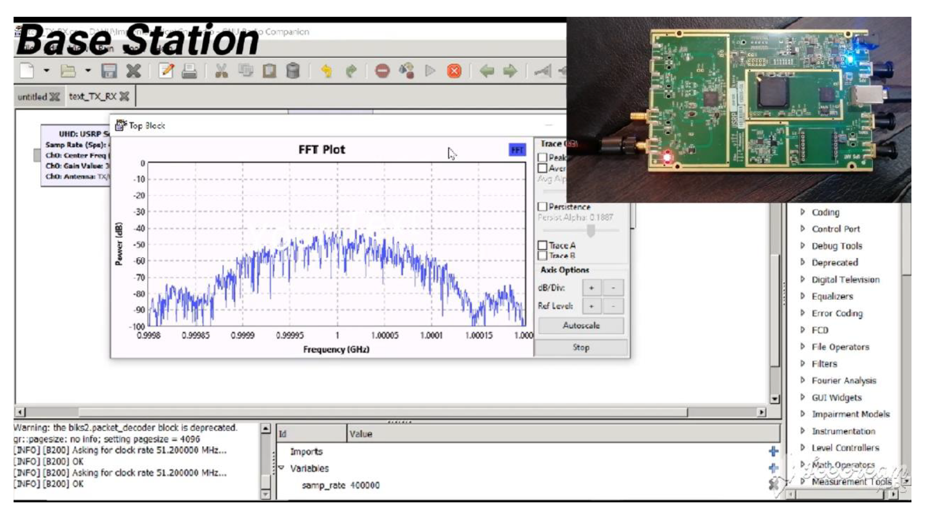
Figure 23, when the USRP of the base station receives the data from the UE1, its red LED turns on, and the FFT plot on GNU Radio has a peak.
Then, when the base station MATLAB code finishes running, two files are generated; one contains the real part of OFDM symbols, and the other contains their imaginary part.
Finally, the USRP of the UE2 receives the data from the base station, as its red LED turns on, and the FFT plot on GNU Radio has a peak as shown in
Figure 24.
6. Conclusions
In this paper, the implementation of the NPDSCH receiver chain and the NPUSCH transmitter chain is presented starting from the algorithm design and passing through the hardware implementation, MATLAB and RTL simulations, and synthesis for each block in the chain. Then, the chain integration is performed, and then MATLAB and RTL are simulated and tested on FPGA Virtex 7. The chain meets all 3GPP NB-IoT LTE standard Release 14 (Rel-14) specifications, and it has a maximum rate of 98.666 Kbps. This rate is calculated according to some assumptions, TBS = 296, including pilots, and coding 1/3, then taking three subframes with respect to the upper layer; therefore, Max Rate = 296/3 ms = 98.666 Kbps and a latency of 1.45 ms. Furthermore, the implementation of the NB-IoT system, comprising two UEs and an implemented NB-IoT base station, is successful, as data sent from one UE to another through the base station are correctly received. As the base station is modeled on MATLAB, the NPUSCH base station receiver receives the data from the FPGA (UE 1), and it passes them to be sent again through the NPDSCH base station transmitter to be received on the receiving FPGA (UE 2). The USRP is used in this model to be the RF part of our system. This model tests the Tx and Rx chains to send different TBSs. The future work is to share more memory resources across the chain, implement soft demodulation and soft decoding to enhance performance, and optimize on the block level, in turn, reducing area and power.
Author Contributions
Data curation, A.A. and R.M.T.; Formal analysis, A.A. and R.M.T.; Methodology, R.M.T., M.S.D. and H.M.; Project administration, H.M.; Supervision, M.S.D. and H.M.; Validation, A.A. and R.M.T.; Visualization, A.A. and R.M.T.; Writing—original draft, A.A., R.M.T. and M.S.D.; Writing—review & editing, M.S.D. and H.M. All authors have read and agreed to the published version of the manuscript.
Funding
This research is supported by Science, Technology, and Innovation Funding Authority (STIFA), Egypt, under grant No. 34876, H. Mostafa received the grant.
Data Availability Statement
This study did not report any data.
Acknowledgments
The authors would like to thank the Opto-Nano-Electronics laboratory (ONE Lab.), Cairo University, and Science, Technology, and Innovation Funding Authority (STIFA), Egypt.
Conflicts of Interest
The authors declare no conflict of interest.
References
- Kaur, K. A survey on internet of things—Architecture, applications, and future trends. In Proceedings of the 2018 First IEEE International Conference on Secure Cyber Computing and Communication (ICSCCC), Jalandhar, India, 15–17 December 2018; pp. 581–583. [Google Scholar]
- Atzori, L.; Iera, A.; Morabito, G. The internet of things: A survey. Comput. Netw. 2010, 54, 2787–2805. [Google Scholar] [CrossRef]
- Is Tech the New Currency? Why You Need Modern, IT. Available online: https://www.insight.com/en_US/content-and-resources/2017/05252017-is-tech-the-new-currency-why-you-need-modern-it.html (accessed on 14 September 2021).
- Raza, U.; Kulkarni, P.; Sooriyabandara, M. Low power wide area networks: An overview. IEEE Commun. Surv. Tutor. 2017, 19, 855–873. [Google Scholar] [CrossRef]
- Kanj, M.; Savaux, V.; Le Guen, M. A tutorial on NB-IoT physical layer design. IEEE Commun. Surv. Tutor. 2020, 22, 2408–2446. [Google Scholar] [CrossRef]
- Rastogi, E.; Saxena, N.; Roy, A.; Shin, D.R. Narrowband Internet of Things: A comprehensive study. Comput. Netw. 2020, 173, 107209. [Google Scholar] [CrossRef]
- Mwakwata, C.B.; Malik, H.; Mahtab Alam, M.; Le Moullec, Y.; Parand, S.; Mumtaz, S. Narrowband Internet of Things (NB-IoT): From physical (PHY) and media access control (MAC) layers perspectives. Sensors 2019, 19, 2613. [Google Scholar] [CrossRef] [PubMed]
- Mekki, K.; Bajic, E.; Chaxel, F.; Meyer, F. Overview of cellular LPWAN technologies for IoT deployment: Sigfox, LoRaWAN, and NB-IoT. In Proceedings of the 2018 IEEE International Conference on Pervasive Computing and Communications Workshops (Percom Workshops), Athens, Greece, 19–23 March 2018; pp. 197–202. [Google Scholar]
- 3GPP. 3GPP TS 36.211, Physical Channels and Modulation (Release 14, v14.11.0); Technical Report. 2021. Available online: https://www.etsi.org/deliver/etsi_ts/136200_136299/136211/14.11.00_60/ts_136211v141100p.pdf (accessed on 1 September 2022).
- 3GPP. 3GPP TS 36.212, Multiplexing and Channel Coding (Release 14, v14.11.0); Technical Report. 2021. Available online: https://www.etsi.org/deliver/etsi_ts/136200_136299/136212/14.11.00_60/ts_136212v141100p.pdf (accessed on 1 September 2022).
- Eladawy, M.; Mostafa, M.; Sameh Said, M.; Mostafa, H. Automated performance-based design technique for an efficient LTE PDSCH implementation using SDSoC tool. Int. J. Commun. Syst. 2020, 33, e4202. [Google Scholar] [CrossRef]
- Mohamed, B.H.; Taha, A.; Shawky, A.; Ahmed, E.; Mohamed, A.; Mohsen, M.; Samy, R.; ELHosiny, A.; Ibrahim, A.; Mostafa, H. Design of the Baseband Physical Layer of NarrowBand IoT LTE Uplink Digital Transmitter. J. Circuits Syst. Comput. 2020, 29, 2050111. [Google Scholar] [CrossRef]
- Divsalar, D.; Pollara, F. Turbo codes for PCS applications. In Proceedings of the IEEE International Conference on Communications ICC ’95, Seattle, WA, USA, 18–22 June 1995; Volume 1, pp. 54–59. [Google Scholar] [CrossRef]
- Lenzi, K.G.; Bianco F., J.A.; de Figueiredo, F.A.; Figueiredo, F.L. Optimized rate matching architecture for a LTE-Advanced FPGA-based PHY. In Proceedings of the 2013 IEEE International Conference on Circuits and Systems (ICCAS), Kuala Lumpur, Malaysia, 18–19 September 2013; pp. 102–107. [Google Scholar] [CrossRef]
- Ikuno, J.C.; Schwarz, S.; Simko, M. LTE rate matching performance with code block balancing. In Proceedings of the 17th European Wireless 2011-Sustainable Wireless Technologies, Vienna, Austria, 27–29 April 2011; VDE: Berlin, Germany, 2011; pp. 1–3. [Google Scholar]
- Yuen, C.H.; Amini, P.; Farhang-Boroujeny, B. Single carrier frequency division multiple access (SC-FDMA) for filter bank multicarrier communication systems. In Proceedings of the 2010 Proceedings of the Fifth International Conference on Cognitive Radio Oriented Wireless Networks and Communications, Cannes, France, 9–11 June 2010; pp. 1–5. [Google Scholar]
- Garrido, M.; Grajal, J.; Sanchez, M.A.; Gustafsson, O. Pipelined Radix-2k Feedforward FFT Architectures. IEEE Trans. Very Large Scale Integr. (VLSI) Syst. 2013, 21, 23–32. [Google Scholar] [CrossRef]
- Ganjikunta, G.K.; Sahoo, S.K. An area-efficient and low-power 64-point pipeline Fast Fourier Transform for OFDM applications. Integration 2017, 57, 125–131. [Google Scholar] [CrossRef]
- He, S.; Torkelson, M. A new approach to pipeline FFT processor. In Proceedings of the International Conference on Parallel Processing, Honolulu, HI, USA, 15–19 April 1996; pp. 766–770. [Google Scholar]
- Qualcomm Incorporated, “NB-PSS and NB-SSS Design,” 3GPP TSG RAN WG1 Ad-Hoc Meeting; Technical Report R1-161981; Qualcomm Incorporated: San Diego, CA, USA, 2016.
- Yang, W.; Hua, M.; Zhang, J.; Xia, T.; Zou, J.; Jiang, C.; Wang, M. Enhanced System Acquisition for NB-IoT. IEEE Access 2017, 5, 13179–13191. [Google Scholar] [CrossRef]
- Prasada, N.; Swaina, A.K.; Mahapatraa, K. FPGA Implementation of Low Latency Scaled CORDIC Based Discrete Fourier Transform Core. In Proceedings of the International Conference on Emerging Trends in Electrical, Communication and Information Technologies, Anantapur, India, 21–23 December 2012; pp. 67–72. [Google Scholar]
- Babu, K.V.; Reddy, G.R.; Gupta, S.; Sharma, U.; Pratik, P. Study and analysis of various frequency offset correction schemes in orthogonal frequency division multiplexing (OFDM) based long term evaluation (LTE) systems 2012. In Proceedings of the Fourth International Conference on Advances in Recent Technologies in Communication and Computing (ARTCom2012), Bangalore, India, 19–20 October 2012; pp. 214–217. [Google Scholar]
- Meher, P.K.; Park, S.Y. Design of Cascaded CORDIC Based on Precise Analysis of Critical Path. Electronics 2019, 8, 382. [Google Scholar] [CrossRef]
- Saeed, M.; Kamal, H.; El-Ghoneimy, M. Novel type-2 fuzzy logic technique for handover problems in a heterogeneous network. Eng. Optim. 2017, 21, 1533–1543. [Google Scholar] [CrossRef]
- Garrido, M. Evolution of the Performance of Pipelined FFT Architectures Through the Years. In Proceedings of the 2020 XXXV Conference on Design of Circuits and Integrated Systems (DCIS), Segovia, Spain, 18–20 November 2020; pp. 1–6. [Google Scholar] [CrossRef]
- Philipov, P.; Lazarov, V.; Zlatev, Z.; Ivanova, M. A Parallel Architecture for Radix-2 Fast Fourier Transform. In Proceedings of the IEEE John Vincent Atanasoff 2006 International Symposium on Modern Computing, JVA ’06, Sofia, Bulgaria, 3–6 October 2006; pp. 229–234. [Google Scholar] [CrossRef]
- Wang, Y.P.E.; Lin, X.; Adhikary, A.; Grovlen, A.; Sui, Y.; Blankenship, Y.; Bergman, J.; Razaghi, H.S. A Primer on 3GPP Narrowband Internet of Things. IEEE Commun. Mag. 2017, 55, 117–123. [Google Scholar] [CrossRef]
- Design and Implementation of Transmitter Chain for Machine Type Communication on LTE Networks. Bachelor’s Dissertation, Indian Institute of Technology, Kanpur, India, 2014.
- Abd Elkader, H.M.; Mabrouk, G.; El-Dien, A.T.; Saad, R.S. Performance of LTE channel estimation algorithms for different interpolation methods and modulation schemes. Int. J. Eng. Res. Dev. 2014, 10, 48–52. [Google Scholar]
- Krasowski, P.; Troha, D. Wireless System Design: NB-IoT Downlink Simulator. Ph.D. Dissertation, Uppsala University, Uppsala, Sweden, 2017. [Google Scholar]
- 3GPP. 3GPP TS 36.104, Evolved Universal Terrestrial Radio Access (E-UTRA); Base Station (BS) Radio Transmission and Reception (Release 14, v14.11.0); Technical Report. 2021. Available online: https://www.etsi.org/deliver/etsi_ts/136100_136199/136104/14.11.00_60/ts_136104v141100p.pdf (accessed on 1 September 2022).
- Spanos, A.; Gioulekas, F.; Birbas, M.; Vgenis, A. Reduced complexity rate-matching/de-matching architecture for the LTE turbo code. In Proceedings of the 2014 21st IEEE International Conference on Electronics, Circuits and Systems (ICECS), Marseille, France, 7–10 December 2014; pp. 411–414. [Google Scholar]
- 3GPP. 3GPP TS 36.212, Evolved Universal Terrestrial Radio Access (E-UTRA); Physical Layer Procedures (Release 14, v14.11.0); Technical Report. 2021. Available online: https://www.etsi.org/deliver/etsi_ts/136200_136299/136212/14.11.00_60/ts_136212v141100p.pdf (accessed on 1 September 2022).
- Salim, A. Evaluation of Word Length Effects on Multistandard Soft Decision Viterbi Decoding. Master Dissertation, Linkoping University, Linkoping, Sweden, 2011. [Google Scholar]
- MathWorks. NB-IoT NPDSCH Block Error Rate Simulation. Available online: https://www.mathworks.com/help/lte/ug/nb-iot-npdsch-block-error-rate-simulation.html (accessed on 14 September 2021).
Figure 2.
CRC block diagram [
12].
Figure 2.
CRC block diagram [
12].
Figure 4.
Block diagram of the channel interleaver unit.
Figure 4.
Block diagram of the channel interleaver unit.
Figure 5.
FFT resource sharing.
Figure 5.
FFT resource sharing.
Figure 6.
IFFT detailed block diagram.
Figure 6.
IFFT detailed block diagram.
Figure 7.
The coarse synchronization procedure.
Figure 7.
The coarse synchronization procedure.
Figure 8.
Illustration of the sign-based buffers partitioning and the single-symbol buffer. (a) The derivation of buffers’ sign-pattern from code cover. (b) The operation of the single-symbol buffer.
Figure 8.
Illustration of the sign-based buffers partitioning and the single-symbol buffer. (a) The derivation of buffers’ sign-pattern from code cover. (b) The operation of the single-symbol buffer.
Figure 9.
FFT detailed block diagram.
Figure 9.
FFT detailed block diagram.
Figure 10.
REM detailed block diagram.
Figure 10.
REM detailed block diagram.
Figure 11.
Channel estimation block diagram.
Figure 11.
Channel estimation block diagram.
Figure 12.
Equalizer block diagram.
Figure 12.
Equalizer block diagram.
Figure 13.
Rate de-matcher block diagram.
Figure 13.
Rate de-matcher block diagram.
Figure 15.
RTL BER vs. SNR.
Figure 15.
RTL BER vs. SNR.
Figure 16.
The block diagram for the implemented NB-IoT system.
Figure 16.
The block diagram for the implemented NB-IoT system.
Figure 17.
Architecture of USRP.
Figure 17.
Architecture of USRP.
Figure 19.
GRC flowgraph of the receiving uplink.
Figure 19.
GRC flowgraph of the receiving uplink.
Figure 20.
GRC flowgraph of the transmitting downlink.
Figure 20.
GRC flowgraph of the transmitting downlink.
Figure 21.
GRC flowgraph of the receiving downlink. (a) For receiving the file of the real components of data. (b) For receiving the file of the imaginary components of data.
Figure 21.
GRC flowgraph of the receiving downlink. (a) For receiving the file of the real components of data. (b) For receiving the file of the imaginary components of data.
Figure 22.
NB-IoT Hardware Setup.
Figure 22.
NB-IoT Hardware Setup.
Figure 23.
Receiving data on the base station.
Figure 23.
Receiving data on the base station.
Figure 24.
Receiving data on the second UE (UE2).
Figure 24.
Receiving data on the second UE (UE2).
Table 1.
VIVADO utilization for Virtex 7 for whole chain.
Table 1.
VIVADO utilization for Virtex 7 for whole chain.
| Resouce | Utilization | Available | Utilization (%) |
|---|
| LUT | 50,728 | 433,200 | 11.71 |
| LUTRAM | 3016 | 174,200 | 1.73 |
| FF | 31,896 | 866,400 | 3.68 |
| BRAM | 69 | 1470 | 4.69 |
| DSP | 80 | 3600 | 2.22 |
| IO | 4 | 850 | 0.47 |
Table 2.
NB-IoT hardware setup components.
Table 2.
NB-IoT hardware setup components.
| (1) and (A) | The USRP and the FPGA of the UE1, respectively |
| (2) and (B) | The USRP and the FPGA of the UE2, respectively |
| (3) | The USRP of the base station |
| Disclaimer/Publisher’s Note: The statements, opinions and data contained in all publications are solely those of the individual author(s) and contributor(s) and not of MDPI and/or the editor(s). MDPI and/or the editor(s) disclaim responsibility for any injury to people or property resulting from any ideas, methods, instructions or products referred to in the content. |
© 2023 by the authors. Licensee MDPI, Basel, Switzerland. This article is an open access article distributed under the terms and conditions of the Creative Commons Attribution (CC BY) license (https://creativecommons.org/licenses/by/4.0/).
