Abstract
The excellent performance and radiation-hardness potential of carbon nanotube (CNT) field effect transistors (CNTFETs) have attracted wide attention. However, top-gate structure CNTFETs, which are often used to make high-performance devices, have not been studied enough. In this paper, the total ionizing dose (TID) effect of the top-gate structure CNTFETs and the influence of the substrate on top-gate during irradiation are studied. The parameter degradation caused by the irradiation- and radiation-damage mechanisms of the top-gate P-type CNTFET were obtained by performing a Co-60 γ-ray irradiation test. The results indicate that the transfer curves of the top-gate P-type CNTFETs shift negatively, the threshold voltage and the transconductance decrease when TID increases, and the subthreshold swing decreases first and then increases with the increase in TID. The back-gate transistor is constructed by using the substrate as a back-gate, and the influence of back-gate bias on the characteristics of the top-gate transistor is tested. We also test the influence of TID irradiation on the characteristics of back-gate transistors, and reveal the effect of trapped charge introduced by radiation on the characteristics of top-gate transistors. In addition, the CNTFETs that we used have obvious hysteresis characteristics. After irradiation, the radiation-induced trapped charges generated in oxide and the OH groups generated by ionization of the CNT adsorbates aggravate the hysteresis characteristics of CNTFET, and the hysteresis window increases with the increase in TID.
1. Introduction
Metamaterial is an artificial material that does not exist in nature. It exhibits material properties not seen in nature, such as permittivity, a bulk modulus or refractive index, which surpasses substances found in nature [1]. In recent years, due to their unique properties, metamaterials have been applied to epsilon-negative metamaterial (ENM), biosensors, metamaterial platforms, and other aspects [2,3,4,5,6], which have developed rapidly in various fields and attracted wide attention.
The development of silicon-based semiconductor technology follows Moore’s law, i.e., the physical size of transistors approaches the limit, and performance hits the bottleneck. Semiconductor devices have entered the post-Moore era, more noticeably than in the Moore era, as new materials and new technology have emerged. Carbon nanotube (CNT) has attracted attention as a metamaterial with excellent properties. A carbon-based device based on carbon nanotube materials has the characteristic of high energy efficiency, with ease of three-dimensional heterogeneous integration, it is low cost, and so on. It is an important technical route to continue Moore’s law, and it has been considered a promising technology in aerospace and other fields [7,8,9,10,11,12,13].
Devices with improved performance and reliability are needed to cope with the radiation effects in space applications. Carbon-based devices show better performance and radiation-hardness than silicon-based devices [14,15,16]. Carbon-based devices have great potential in space applications, such as space SRAM and radiation-hardness IC. Furthermore, due to its excellent electrical performance and special physical structure, CNTFET has undergone rapid development in flexible electronic devices [17], which can be applied to wearable electronic devices for the human body and space environment detection devices in space stations in the future.
The carbon nanotube field effect transistor (CNTFET) is the basic unit of a carbon-based integrated circuit. The channel region of CNTFET is composed of CNT. CNTFET can be divided into various types according to different processes and structures, including back-gate structure, top-gate structure, ion gel gate structure, etc. In space applications, CNTFET will face radiation damage effects caused by high-energy particles, resulting in the degradation of device performance. The total ionizing dose effect (TID) is one of the most important radiation damage effects.
Researchers have studied the TID effect on CNTFETs with different structures. Cory D. Cress et al. used a Co-60 γ-ray source to conduct a TID test on P-type back-gate CNTFET without a passivity layer [18]. The results indicated that irradiation did not generate significant damage to the CNT channel, and it was believed that the change of device characteristics mainly depended on materials around CNT, interface state, and air environment. Yudan Zhao et al. further investigated the influence of CNT absorbability and CNT arrangement on the TID effect of back-gate CNTFET. They demonstrated that the air molecules adsorbed by CNT in devices without a passivation layer, the fixed charge in materials of the passivation layer, and the improvement of the contact junction in network arrangement were the predominant factors influencing the TID effect of CNTFET [19].
In recent years, Lian-Mao Peng‘s team researched the radiation effect of ion gel gate CNTFET, and the results indicated that the structure of the ion gel gate could protect the channel of CNT, improved the radiation tolerance effectively [16,20,21], and could be recovered by annealing after irradiation. However, the author also mentioned that the structure suffers from low performance, difficulty in scaling down, and a narrow range of operating temperatures.
Compared with the first two structures, the top-gate device can not only protect the channel of CNT effectively and enhance the radiation tolerance of CNTFET, but can also reduce the size of the device more easily, which can be used for high-performance carbon nanotube devices [22,23,24]. In 2019, Xinyang Zhao et al. studied the TID effect of a flexible top-gate carbon nanotube thin-film transistor (CNTFT) using Co-60 γ-ray. The research showed that the radiation resistance of flexible CNTFETs was comparable to that of rigid CNTFETs, which were fabricated on the oxide substrate [25]. For the TID of rigid CNTFET, Maguang Zhu et al. conducted research on the TID of SRAM composed of top-gate CNTFET [26]. In addition, they tested TID on each part of the top-gate CNTFETs independently [15]. The results showed that CNTs are a kind of radiation-hardened semiconducting material, and the damage of substrate material and gate oxide material was the main factor of TID. However, it did not reveal the influence process of radiation-induced trapped charge in the substrate material on the characteristics of the top-gate transistor. Up to now, there has been little research on the sensitivity parameters, damage rules, and mechanisms of top-gate CNTFETs, and relevant research is urgently required for the design of CNT-based devices.
In this paper, we researched TID of P-type CNT-network FETs with a top-gate structure. The variation of threshold voltage, transconductance, subthreshold swing, and hysteresis characteristics of the device before and after irradiation by Co-60 γ-ray are analyzed. The influence mechanism of trapped charge introduced by TID irradiation on the characteristics of the top-gate CNTFETs is discussed. Additionally, the influence of back-gate pressure on front-gate transfer characteristic curves (IDS-VGS) and its control ability were tested. Finally, the possible reasons for CNTFETs hysteresis and the relationship of hysteresis characteristics with TID are explained.
2. Device Structures and Experimental Details
The structure of the test samples used in this paper is shown in Figure 1a. The CNTFET substrates are Si and SiO2. The Si substrate is 500 μm thick, and the SiO2 substrate is 280 nm thick. The carbon tube material comprises a reticulated film with a density of 15 pieces/um. The device image is shown in Figure 1b. The semiconducting CNT-network films are the channel regions of the devices. CNT films are undoped, and the width/length ratio is 30 μm/4 μm. The Pd layers serve as electrodes. The function of the P-type transistor is obtained according to the difference of work function between Pd and CNT. The contacts between CNTs and Pd electrodes are Ohmic contacts, which was detected by testing the IDS-VDS characteristics of the device. The gate oxide layers consisted of high-k materials Y2O3 and HfO2, which are 10 nm in total. Samples are wafer-level unpackaged devices.
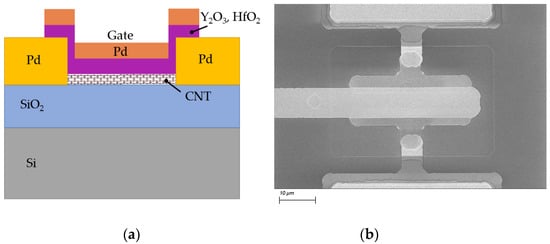
Figure 1.
(a) Structure of the top-gate CNTFET; (b) SEM of the top-gate CNTFET.
The irradiation experiments were carried out on a Co-60 γ-ray source in Xinjiang Technical Institute of Physics and Chemistry, Chinese Academy Sciences. The average energy of γ ray is 1.25 MeV, and the devices are irradiated in atmospheric environment. The dose rate is 195.476 rad(Si)/s during irradiation. Dose levels are 200 k rad(Si), 500 k rad(Si), 1 M rad(Si), 2 M rad(Si), and 3 M rad(Si). The total irradiation cumulative time is 255 min 47 s. The accumulation time of each dose level was 17 min 3 s, 25 min 35 s, 42 min 38 s, 85 min 16 s, and 85 min 16 s, respectively. During irradiation, devices are floating. Co-60 γ-ray has a dose-building area when it propagates in the medium [27], and there might be a dose error in the sensitive area because the devices that we used were not packaged. In order to ensure uniformity of the absorbed dose during irradiation, a pre-balanced layer of about 5 mm was added in front of the devices, and a backscatter layer of about 2 cm was added behind the devices to ensure balance of secondary electrons and the absorbed dose in the sensitive area.
Devices were measured using the probe station and the Keithley 4200SCS parameter analyzer at room temperature. The measurement included the IDS-VGS characteristic curves of the linear region and saturated region. The order of scanning may affect the hysteresis characteristics as the gate voltage (VGS) sweeps from 0.5 V to −2 V, with the −0.02 V step first, and from −2 V to 0.5 V. The test information is shown in Table 1. In order to avoid the effect of annealing on the devices, the test time of each dose level is less than 45 min.

Table 1.
Measurement information in this paper.
3. Results and Discussion
3.1. Effect of TID Radiation on IDS-VGS Characteristics of Top-Gate CNTFET
Figure 2 shows the IDS-VGS curves under different irradiation doses. It can be seen from Figure 2 that the IDS-VGS characteristics shift negatively after TID radiation, and the saturation current in the linear region decreases with the increase in TID.
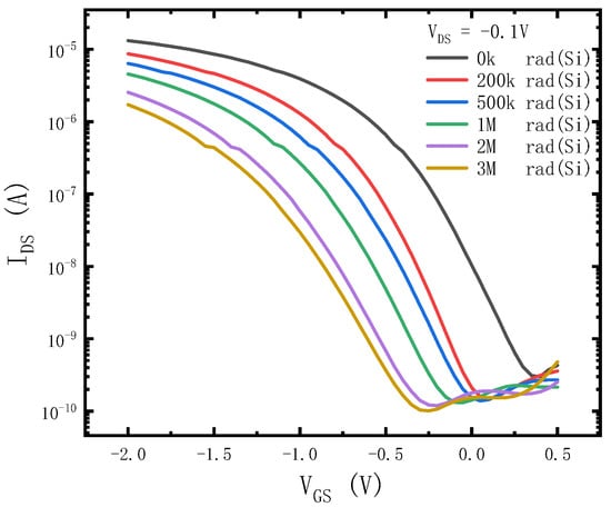
Figure 2.
Transfer characteristic curves after irradiation.
The threshold voltage (), maximum transconductance (), and subthreshold swing (SS) of the devices before and after irradiation were extracted from the IDS-VGS curves, as shown in Figure 3a, Figure 3b and Figure 3c, respectively. As can be seen from the figure, with the increase in accumulated doses of irradiation, shifts negatively and decreases monotonically, while the subthreshold swing (SS) first decreases and then increases.
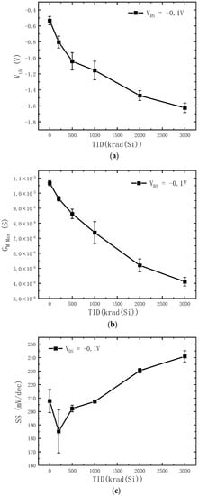
Figure 3.
The changes of (a) threshold voltage (), (b) maximum transconductance (GM Max) and (c) subthreshold swing (SS) after irradiation.
The relation between threshold voltage and trapped charges induced by radiation is [28,29]:
where is the threshold voltage before irradiation, is the charge variation of the top-gate oxide layer, is the change in the interface-trapped charges, and is the capacitance of the top-gate oxide layer. Equation (1) demonstrated that both radiation-induced oxide-trapped charge and interface-trapped charge could lead to threshold voltage shift.
Equation (2) is the formula of transconductance:
Equation (3) is the formula of subthreshold swing:
where is the carrier mobility, is the depletion capacitance, is the interface trap capacitance, is Boltzmann constant, is temperature, and is electronic charge. Carrier mobility is determined as follows:
Interface trap capacitance is obtained with Equation (5):
where is the mobility pre-irradiation, is the radiation dependent densities of trapped charges in interface SiO2/CNT, is the parameter reflecting the technology change, and is the density of interface traps.
The transconductance is proportional to the carrier mobility, while the carrier mobility is mainly affected by the interface traps. Therefore, an increase in irradiation dose increases interface traps, which then results in Coulomb scattering that in turn affects carrier mobility in the channel, and eventually causes a decrease in the maximum transconductance of the device.
Both depletion capacitance and interface trap capacitance could affect subthreshold swing. However, CNTs are ultrathin channel materials while can be neglected [15]. The subthreshold swing of CNTFETs is thus only affected by , and the density of interface traps is the main influencing factor for from Equation (5).
Because we used a CNT-network FET, CNTs in the channel region are staggered, and there is a large number of junctions between CNTs in the network films. According to previous research, high energy γ-ray can produce defects near CNT junctions. Through annealing under γ irradiation [30] or the oxidation of CNT due to the ionization effect [31,32], CNT junctions can recombine with nearby defects, improving the performance of CNT [19,33] that repairs the interface traps on the surface of CNT, and reduces the density of interface traps to a certain degree. Therefore, at the initial stage of radiation, that is from 0 k rad (Si) to about 200 k rad (Si), the recombination process of CNT junctions that can repair interfacial traps plays a major role, and the subthreshold swing of CNTFET decreases with the increase in TID. With the increase in TID, the number of junctions begins to decrease, and interface traps become the dominant factor, which increases the subthreshold swing with the increase in TID.
Considering the above reasons, the negative shift of IDS-VGS characteristics in Figure 2 can be confirmed to be caused by radiation. During irradiation, electron hole pairs are generated in the gate dielectric layer and/or oxide substrate, and the hole mobility is relatively low, which is easily captured by oxide and interface traps, forming positive trapped charges and requiring a higher negative gate voltage to control the channel. Therefore, as TID increases, the negative shift of the I–V curve occurs.
3.2. Influence of Trapped Charges in SiO2 Substrate Induced by Irradiation on Top-Gate CNTFET Characteristics
With regard to the devices in this paper, theoretically, the TID can generate trapped charges in both the top-gate dielectric layer and the substrate oxide, leading to degradation of the device parameters. In order to determine where the trapped charges were the dominant factor, we measured the IDS-VGS characteristics of the devices under different substrate voltages.
As shown in Figure 4, positive voltages were applied to the substrate in order to simulate the effect of the substrate’s accumulated oxide-trapped charges on top-gate transistors. With the increase in the substrate voltage, the IDS-VGS curve shifts negatively and the saturation current decreases gradually, which is consistent with the phenomenon observed in radiation. It is shown that the positive oxide-trapped charges are also generated in the substrate under γ-ray irradiation, which is consistent with the effect of trapped charges generated in gate on the IDS-VGS characteristics.
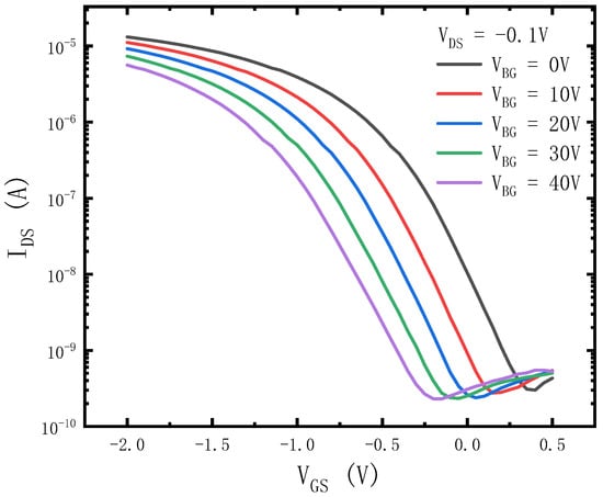
Figure 4.
IDS-VGS characteristics of devices at different substrate voltages.
Figure 5a–c shows the threshold voltage, the maximum transconductance, and the subthreshold swing of top-gate transistor under various back-gate voltages, respectively. It may be assumed that positive oxide-trapped charges in the substrate bring holes closer to the surface of the CNT channel and increase the generation of interface traps. As a result, transconductance decreases and subthreshold swing increases when the substrate voltage is increased. On the other hand, Figure 5b also shows that the phenomenon of the subthreshold swing decreasing first and then increasing during irradiation, as shown in Figure 3c, derives from other factors rather than interface-trapped charges.
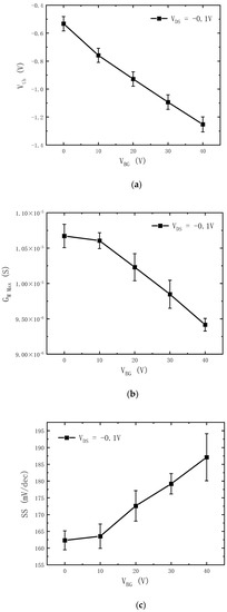
Figure 5.
(a) The changes of threshold voltage under various substrate voltages. (b) Influence of different substrate voltages on transconductance. (c) The effect of different substrate voltages on subthreshold swing.
In addition, we used the substrate as the back-gate to test the TID radiation effect on the characteristics of the back-gate transistor. Figure 6 shows the IDS-VBG characteristic curves of the back-gate transistor at different TIDs. Figure 6 also shows that the IDS-VBG characteristic curves of the back-gate transistor shift negatively, and the saturation current decreases, which is consistent with the front-gate characteristic curves in Figure 2. The threshold voltage of the back-gate transistor is also extracted by the constant voltage method, as shown in Figure 7. In the same figure, it can be seen that the threshold voltage of the back-gate transistor changes obviously. It is supposed that there will be many oxide-trapped charges in the substrate that are induced by irradiation.
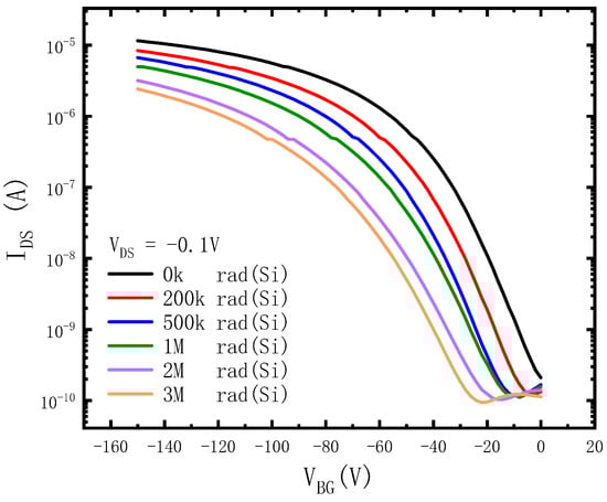
Figure 6.
IDS-VBG characteristics of the back-gate after irradiation.
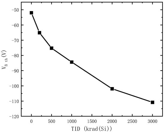
Figure 7.
Threshold voltage of the back-gate transistor after irradiation.
Figure 8 shows the coupling coefficient between the back-gate transistor and the front-gate transistor. The device coupling coefficient is almost linear, indicating that the back-gate has better control over the front-gate, the density of trapped charges near the interface is low, and the TID effect has little influence on the coupling effect for the test samples in this paper.
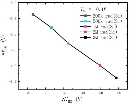
Figure 8.
Changes of coupling coefficient.
3.3. TID Influence on Hysteresis Characteristics of Top-Gate CNTFET
For field effect transistors, the stable control of voltage to current is an important index of device performance. The hysteresis characteristics will affect the stability of the device, and it will pose a problem that should be discussed when CNTFET is used in real life.
The channel of CNTFET is composed of organic material CNTs, and the interface becomes complicated when it comes into contact with inorganic materials. Meanwhile, high-k materials such as that are used as the gate dielectric have more defects than . This will more likely generate current hysteresis characteristics [34]. Thus, we measured the hysteresis characteristics through bidirectional scanning for gate voltage, as shown in Figure 9. The maximum gate voltage difference under the same drain current was used to define the hysteresis window . The test sequence involves scanning of the gate voltage VGS from 0.5 V to −2 V, which is defined as negative scanning in this paper. Subsequently, it is scanned back from −2 V to 0.5 V, which is defined as positive scanning in this paper. It can be clearly seen from Figure 9 that the hysteresis window, , increased with the increase in TID.
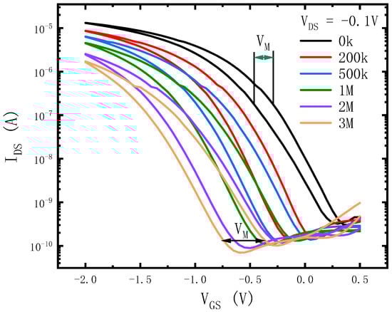
Figure 9.
Hysteresis characteristics as a function of TID.
Previous research has shown that the reasons for the hysteresis of devices are mainly due to the following four kinds of charges [35,36,37]: (1) positive oxide fixed charge that is generally very close to the channel (about 2 nm); (2) oxide-trapped charge; (3) interface-trapped charge; and (4) moving charge in oxide. Due to the properties of high-k materials, there are more fixed positive charges in than in . As mentioned in the previous analysis, the generation of oxide-trapped charge and interfacial trapped charge are consistent with the change of hysteresis characteristics with the accumulation of TID. Therefore, the overall quantity of oxide-trapped charges and interfacial trapped charges increases with the increase in TID and could generate the change of hysteresis characteristics. The hysteresis characteristics are proportional to TID.
On the other hand, CNTFETs are different from traditional transistors. CNTs have strong adsorption, and it is difficult to avoid the adsorption of oxygen, molecules of water, and other impurities in the fabrication process. At present, it is widely believed that water molecules adsorbed by CNT and the presence of OH group in the form of silanol are the main sources of hysteresis characteristics in CNTFETs [38]. Water molecules and groups will trap electrons in CNTs and induce excess holes in the channel, resulting in the transistor current becoming larger than expected under the condition of the same VGS. When the VGS scans negatively in the measurement process, the negative gate voltage leads to the electrons captured by the water molecules and the groups being gradually released. Therefore, the transistor current becomes smaller under the same gate voltage VGS condition when scanning back. This phenomenon will be exacerbated by the process of irradiation. The water molecules that are adsorbed on the surface of the CNTs are ionized during Co-60 γ-ray irradiation and produce more OH groups. In this way, the electron capture and release of adsorbates on the CNT surface becomes more intense, which further exacerbates the hysteresis characteristics of CNTFETs.
4. Conclusions
CNTFETs have been considered to be some of the most promising candidates for continuing Moore’s law and have received much attention in the aerospace field. The TID effect of CNTFET has been the focus of much research. In different device structures, the top-gate structure is an important CNTFET structure. It is used to manufacture high-performance CNTFETs because it scales down easily. However, the lack of studies on TID of the top-gate structure CNTFET restricts the development of radiation-hardness top-gate CNTFETs.
In this paper, the effect of radiation-induced trapped charges on the top-gate CNTFET characteristics is studied. Firstly, we measure the change of IDS-VGS characteristics in the top-gate transistors with the total dose increases, and show that radiation could induce oxide-trapped charges and interface-trapped charges in the CNTFET. They lead to a negative shift in the transistor IDS-VGS characteristics. Both oxide-trapped charges and interface-trapped charges lead to the threshold voltage shifting negatively. The interface-trapped charges not only affect the threshold voltage, but also reduce the mobility of carriers. This results in the transconductance reduction with the increase in TID. In addition to the influence of interface-trapped charges, the subthreshold swing is also affected by CNT junctions in the channel. During irradiation, a large number of CNT junctions recover, and some interface traps are repaired, which is the main factor affecting the subthreshold swing at the initial stage of irradiation. With the reduction in CNT junctions, the accumulation of interface-trapped charges has become the main factor affecting the subthreshold swing. Thus, the subthreshold swing decreases first and then increases. In order to confirm the source and influence of radiation-induced trapped charges, we construct back-gate transistors, test the effect of different back-gate voltages on the front-gate IDS-VGS characteristics, and obtain the TID influence on the back-gate transistor characteristics. We also extract the coupling coefficient between the back-gate transistor and the front-gate transistor. The results indicate that the TID has little effect on the coupling coefficient, and the back-gate has better control ability on the front-gate of the samples. Finally, in the research of hysteresis characteristics, the results show that the hysteresis characteristics of CNTFETs increased with the increase in oxide-trapped charges and interface-trapped charges after radiation. Furthermore, the hysteresis characteristics of CNTFETs significantly increased following adsorbates ionization on the surface of the CNT channel. In general, the hysteresis characteristics of CNTFETs are proportional to TID.
The ultimate purpose of the TID study of CNTFETs is to apply this to the space environment, where the particle situation is complex and the radiation dose rate is low. Different particles and dose rates may cause different phenomena. To estimate the impact of the actual environment as accurately as possible, radiation conditions that are closer to the actual application environment could be considered in future research, namely different radiation sources and low dose rates of radiation exposure. In addition, a quantitative analysis of trap charge is also necessary. As the technology of CNTFETs develops, trap charge can be extracted by devices with better subthreshold swing characteristics [39,40], which is helpful in the development of anti-irradiation technology of CNTFET.
Author Contributions
Conceptualization, J.C., Q.Z.; methodology, H.D., J.C., Q.Z. and C.H.; validation, H.D., J.C. and Q.Z.; formal analysis, H.D.; investigation, H.D., J.C., M.X. and G.Y.; resources, H.X. and N.G.; data curation, H.D.; writing—original draft preparation, H.D.; writing—review and editing, H.D. and J.C.; visualization, H.D.; supervision, Y.L., Q.G.; project administration, J.C.; funding acquisition, J.C. All authors have read and agreed to the published version of the manuscript.
Funding
This research was supported in part by the Youth Innovation Promotion Association CAS (2020430), the West Light Foundation of the Chinese Academy of Science under Grant No. 2019-XBQNXZ-A-003, and the National Natural Science Foundation of China under Grant 12275352.
Institutional Review Board Statement
Not applicable.
Informed Consent Statement
Not applicable.
Data Availability Statement
Data are not available in a publicly accessible repository and they cannot be shared upon request.
Conflicts of Interest
The authors declare no conflict of interest.
References
- Lincoln, R.L.; Scarpa, F.; Ting, V.P.; Trask, R.S. Multifunctional composites: A metamaterial perspective. Multifunct. Mater. 2019, 2, 043001. [Google Scholar] [CrossRef]
- Mohammadi Estakhri, N.; Edwards, B.; Engheta, N. Inverse-designed metastructures that solve equations. Science 2019, 363, 1333–1338. [Google Scholar] [CrossRef] [PubMed]
- Lalegani, Z.; Ebrahimi, S.S.; Hamawandi, B.; La Spada, L.; Batili, H.; Toprak, M.S. Targeted dielectric coating of silver nanoparticles with silica to manipulate optical properties for metasurface applications. Mater. Chem. Phys. 2022, 287, 126250. [Google Scholar] [CrossRef]
- Pacheco-Peña, V.; Beruete, M.; Rodríguez-Ulibarri, P.; Engheta, N. On the performance of an ENZ-based sensor using transmission line theory and effective medium approach. New J. Phys. 2019, 21, 043056. [Google Scholar] [CrossRef]
- Akbari, M.; Shahbazzadeh, M.J.; La Spada, L.; Khajehzadeh, A. The Graphene Field Effect Transistor Modeling Based on an Optimized Ambipolar Virtual Source Model for DNA Detection. Appl. Sci. 2021, 11, 8114. [Google Scholar] [CrossRef]
- Greybush, N.J.; Pacheco-Peña, V.; Engheta, N.; Murray, C.B.; Kagan, C.R. Plasmonic Optical and Chiroptical Response of Self-Assembled Au Nanorod Equilateral Trimers. ACS Nano 2019, 13, 1617–1624. [Google Scholar] [CrossRef]
- Javey, A.; Guo, J.; Wang, Q.; Lundstrom, M.; Dai, H. Ballistic carbon nanotube field-effect transistors. Nature 2003, 424, 654–657. [Google Scholar] [CrossRef]
- Franklin, A.D.; Luisier, M.; Han, S.J.; Tulevski, G.; Breslin, C.M.; Gignac, L.; Lundstrom, M.S.; Haensch, W. Sub-10 nm Carbon Nanotube Transistor. Nano Lett. 2012, 12, 758–762. [Google Scholar] [CrossRef]
- Chen, B.; Zhang, P.; Ding, L.; Han, J.; Qiu, S.; Li, Q.; Zhang, Z.; Peng, L.-M. Highly Uniform Carbon Nanotube Field-Effect Transistors and Medium Scale Integrated Circuits. Nano Lett. 2016, 16, 5120–5128. [Google Scholar] [CrossRef]
- De Volder, M.F.; Tawfick, S.H.; Baughman, R.H.; Hart, A.J. Carbon Nanotubes: Present and Future Commercial Applications. Science 2013, 339, 535–539. [Google Scholar] [CrossRef]
- Yang, Y.; Ding, L.; Chen, H.; Han, J.; Zhang, Z.; Peng, L.M. Carbon nanotube network film-based ring oscillators with sub 10-ns propagation time and their applications in radio-frequency signal transmission. Nano Res. 2018, 11, 300–310. [Google Scholar] [CrossRef]
- Peng, L.M.; Zhang, Z.; Wang, S. Carbon nanotube electronics: Recent advances. Mater. Today 2014, 17, 433–442. [Google Scholar] [CrossRef]
- Yang, L.; Wang, S.; Zeng, Q.; Zhang, Z.; Pei, T.; Li, Y.; Peng, L.M. Efficient photovoltage multiplication in carbon nanotubes. Nat. Photonics 2011, 5, 672–676. [Google Scholar] [CrossRef]
- Liu, L.; Han, J.; Xu, L.; Zhou, J.; Zhao, C.; Ding, S.; Shi, H.; Xiao, M.; Ding, L.; Ma, Z.; et al. Aligned, high-density semiconducting carbon nanotube arrays for high-performance electronics. Science 2020, 368, 850–856. [Google Scholar] [CrossRef]
- Zhu, M.; Zhou, J.; Sun, P.; Peng, L.M.; Zhang, Z. Analyzing Gamma-Ray Irradiation Effects on Carbon Nanotube Top-Gated Field-Effect Transistors. ACS Appl. Mater. Interfaces 2021, 13, 47756–47763. [Google Scholar] [CrossRef]
- Zhu, M.; Xiao, H.; Yan, G.; Sun, P.; Jiang, J.; Cui, Z.; Zhao, J.; Zhang, Z.; Peng, L.-M. Radiation-Hardened and Repairable Integrated Circuits Based on Carbon Nanotube Transistors with Ion Gel Gates. Nat. Electron. 2020, 3, 622–629. [Google Scholar] [CrossRef]
- Li, X.; Wang, X.; Deng, J.; Li, M.; Shao, S.; Zhao, J. Printed carbon nanotube thin film transistors based on perhydropolysilazane-derived dielectrics for low power flexible electronics. Carbon 2022, 191, 267–276. [Google Scholar] [CrossRef]
- Cress, C.D.; McMorrow, J.J.; Robinson, J.T.; Friedman, A.L.; Landi, B.J. Radiation Effects in Single-Walled Carbon Nanotube Thin-Film-Transistors. IEEE Trans. Nucl. Sci. 2010, 57, 3040–3045. [Google Scholar] [CrossRef]
- Zhao, Y.; Li, D.; Xiao, L.; Liu, J.; Xiao, X.; Li, G.; Jin, Y.; Jiang, K.; Wang, J.; Fan, S.; et al. Radiation effects and radiation hardness solutions for single-walled carbon nanotube-based thin film transistors and logic devices. Carbon 2016, 108, 363–371. [Google Scholar] [CrossRef]
- Luo, M.; Zhu, M.; Wei, M.; Shao, S.; Robin, M.; Wei, C.; Cui, Z.; Zhao, J.; Zhang, Z. Radiation-Hard and Repairable Complementary Metal-Oxide-Semiconductor Circuits Integrating printed n-type Indium Oxide and p-type Carbon Nanotube Field-Effect Transistors. ACS Appl. Mater. Interfaces 2020, 12, 49963–49970. [Google Scholar] [CrossRef]
- Wang, Y.; Xiao, L. Repairable Integrated Circuits for Space. Nat. Electron. 2020, 3, 586–587. [Google Scholar] [CrossRef]
- Javey, A.; Kim, H.; Brink, M.; Wang, Q.; Ural, A.; Guo, J.; McIntyre, P.; McEuen, P.; Lundstrom, M.; Dai, H. High-κ dielectrics for advanced carbon-nanotube transistors and logic gates. Nat. Publ. Group 2002, 1, 241–246. [Google Scholar] [CrossRef] [PubMed]
- Pitner, G.; Zhang, Z.; Lin, Q.; Su, S.K.; Gilardi, C.; Kuo, C.; Kashyap, H.; Weiss, T.; Yu, Z.; Chao, T.A.; et al. Sub-0.5 nm Interfacial Dielectric Enables Superior Electrostatics: 65 mV/dec Top-Gated Carbon Nanotube FETs at 15 nm Gate Length. In Proceedings of the 2020 IEEE International Electron Devices Meeting (IEDM), San Francisco, CA, USA, 12–18 December 2020; IEEE: NewYork, NY, USA, 2020; pp. 3.5.1–3.5.4. [Google Scholar]
- Qiu, C.; Zhang, Z.; Xiao, M.; Yang, Y.; Zhong, D.; Peng, L.M. Scaling carbon nanotube complementary transistors to 5-nm gate lengths. Science 2017, 355, 271. [Google Scholar] [CrossRef] [PubMed]
- Zhao, X.; Yu, M.; Cai, L.; Liu, J.; Wang, J.; Wan, H.; Wang, J.; Wang, C.; Fu, Y. Radiation effects in printed flexible single-walled carbon nanotube thin-film transistors. AIP Adv. 2019, 9, 105121. [Google Scholar] [CrossRef]
- Zhu, M.G.; Zhang, Z.; Peng, L.M. High-Performance and Radiation-Hard Carbon Nanotube Complementary Static Random-Access Memory. Adv. Electron. Mater. 2019, 5, 1900313. [Google Scholar] [CrossRef]
- Wang, Y.; Xiang, Z.Q.; Hu, H.F.; Cao, F. Feasibility Study of Semifloating Gate Transistor Gamma-Ray Dosimeter. IEEE Electron Device Lett. 2015, 36, 99–101. [Google Scholar] [CrossRef]
- Petrosjanc, K.O.; Adonin, A.S.; Kharitonov, I.A.; Sicheva, M.V. SOI device parameter investigation and extraction for VLSI radiation hardness modeling with SPICE. In Proceedings of the 1994 IEEE International Conference on Microelectronic Test Structures, San Diego, CA, USA, 22–25 March 1994; pp. 126–129. [Google Scholar]
- Galloway, K.F.; Gaitan, M.; Russell, T.J. A Simple Model for Separating Interface and Oxide Charge Effects in MOS Device Characteristics. IEEE Trans. Nucl. Sci. 1984, 31, 1497–1501. [Google Scholar] [CrossRef]
- Li, B.; Feng, Y.; Ding, K.; Qian, G.; Zhang, X.; Zhang, J. The effect of gamma ray irradiation on the structure of graphite and multi-walled carbon nanotubes. Carbon 2013, 60, 186–192. [Google Scholar] [CrossRef]
- Miao, M.; Hawkins, S.C.; Cai, J.Y.; Gengenbach, T.R.; Knott, R.; Huynh, C.P. Effect of gamma-irradiation on the mechanical properties of carbon nanotube yarns. Carbon 2011, 49, 4940–4947. [Google Scholar] [CrossRef]
- Skakalova, V.; Hulman, M.; Fedorko, P.; Lukáč, P.; Roth, S. Effect of gammairradiation on single-wall carbon nanotube paper. AIP Conf. Proc. 2003, 685, 143–147. [Google Scholar]
- Vitusevich, S.A.; Sydoruk, V.A.; Petrychuk, M.V.; Danilchenko, B.A.; Klein, N.; Offenhäusser, A.; Bosman, G. Transport properties of single-walled carbon nanotube transistors after gamma radiation treatment. J. Appl. Phys. 2010, 107, 063701. [Google Scholar] [CrossRef]
- Leroux, C.; Mitard, J.; Ghibaudo, G.; Garros, X.; Reimbold, G.; Guillaumot, B.; Martin, F. Characterization and modeling of hysteresis phenomena in high K dielectrics. In Proceedings of the IEEE International Electron Devices Meeting, IEDM Technical Digest, San Francisco, CA, USA, 13–15 December 2004; pp. 737–740. [Google Scholar]
- Schroder, D.K. Semiconductor Material and Device Characterization, 3rd ed.; John Wiley & Sons, Inc.: Hoboken, NJ, USA, 2006. [Google Scholar]
- Kessler, J.O.; Tompkins, B.E.; Blanc, J. Variable-characteristic p-n-junction devices based on reversible ion drift. Solid-State Electron. 1963, 6, 297–307. [Google Scholar] [CrossRef]
- Snow, E.H.; Grove, A.S.; Deal, B.E.; Sah, C.T. Ion Transport Phenomena in Insulating Films. J. Appl. Phys. 1965, 36, 1664–1673. [Google Scholar] [CrossRef]
- Kim, W.; Javey, A.; Vermesh, O.; Wang, Q.; Li, Y.; Dai, H. Hysteresis Caused by WaterMolecules in Carbon Nanotube Field-Effect Transistors. Nano Lett. 2003, 3, 193–198. [Google Scholar] [CrossRef]
- Patil, P.D.; Ghosh, S.; Wasala, M.; Lei, S.; Vajtai, R.; Ajayan, P.M.; Ghosh, A.; Talapatra, S. Gate-Induced Metal–Insulator Transition in 2D van der Waals Layers of Copper Indium Selenide Based Field-Effect Transistors. ACS Nano 2019, 13, 13413–13420. [Google Scholar] [CrossRef] [PubMed]
- ASTM F996-11; Standard Test Method for Separating an Ionizing Radiation-Induced Mosfet Threshold Voltage Shift into Components Due to Oxide Trapped Holes and Interface States Using the Subthreshold Current-Voltage Characteristics. ASTM International: West Conshohocken, PA, USA, 2011.
Disclaimer/Publisher’s Note: The statements, opinions and data contained in all publications are solely those of the individual author(s) and contributor(s) and not of MDPI and/or the editor(s). MDPI and/or the editor(s) disclaim responsibility for any injury to people or property resulting from any ideas, methods, instructions or products referred to in the content. |
© 2023 by the authors. Licensee MDPI, Basel, Switzerland. This article is an open access article distributed under the terms and conditions of the Creative Commons Attribution (CC BY) license (https://creativecommons.org/licenses/by/4.0/).