Abstract
This paper proposes a circuit model of a cross-coupled CMOS AC–DC charge pump (XC–CP) operating in the subthreshold region. The aim is to improve the efficiency of designing XC–CPs with a variety of specifications, e.g., input and output voltages and AC input frequency. First, it is shown that the output resistance (Ro) of XC–CP is much higher than those of CPs with single diodes (SD–CP) and ultra-low-power diodes (ULPD–CP) as charge transfer switches (CTSs). Second, the reason behind the above feature of XC–CP, identified by a simple model, is that the gate-to-source voltages of CTS MOSFETs are independent of the output voltage of the CP. Third, the high but finite Ro of XC–CP is explainable with a more accurate model that includes the dependence of the saturation current of MOSFETs operating in the subthreshold region on the drain-to-source voltage, which is a function of the output voltage of CP. The model is in good agreement with measured and simulated results of XC–, SD–, and ULPD–CPs fabricated in a 250 nm CMOS.
1. Introduction
AC–DC charge pumps (CPs) are used to convert AC input power to DC output power for microwave wireless power transmission (MWPT) or RF energy harvesting (RF–EH) [1,2,3,4,5,6,7,8,9,10,11], biomedical applications [12,13,14,15,16], and vibration energy harvesting [17,18,19,20], as shown in Figure 1a–c. Figure 1d illustrates a block diagram of a CP composed of multiple rectifiers and capacitors connected in series between the input and output terminals. The capacitors are driven by the differential signals CLK and CLKB alternately. A filtering capacitor is connected to the output terminal to generate a DC voltage. The DC voltage is used for the following circuit blocks or ICs, such as sensors and RF ICs in IoT edge modules or medical devices. The rectifier used in AC–DC CPs was originally a diode-connected single MOSFET [21,22,23], as shown in Figure 2a. When the amplitude of the input AC voltage is low in low-power systems, reverse leakage becomes a significant concern. To reduce the reverse leakage current, ultra-low-power diodes were proposed and used in low-power AC–DC CPs [24,25,26], as shown in Figure 2b. To boost the gate voltages of switching MOSFETs for increasing the forward current, cross-coupled CMOS or CMOS latches have been widely used [27,28,29,30,31,32,33,34], as shown in Figure 2c.
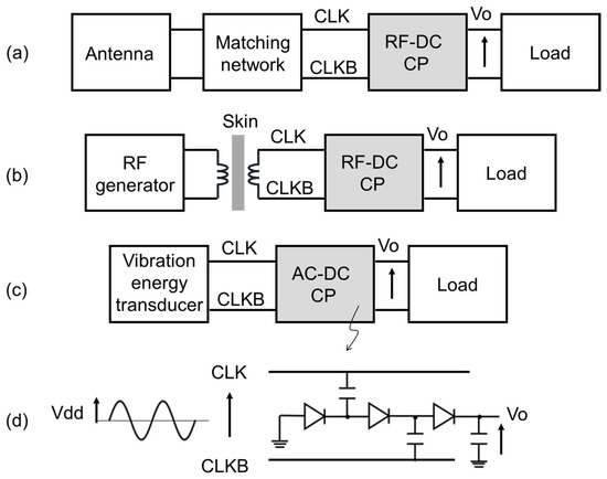
Figure 1.
Applications of AC–DC/RF–DC CPs (a) Microwave wireless power transmission or RF energy harvesting, (b) biomedical application, (c) vibration energy harvesting) and (d) block diagram of CP.
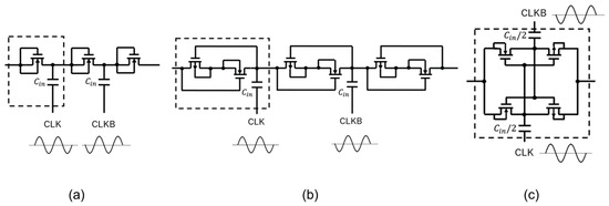
Figure 2.
AC–DC CPs with diode-connected MOSFETs (a), ultra-low-power diodes (ULPDs) (b), and cross-coupled CMOS or CMOS latch (c).
The frequency of AC signals is spread depending on the use cases. MWPT utilizes ISM bands such as 920 MHz [1,2,3], 2.4 GHz [4,5,6,7], 5.8 GHz [8,9], and 24 GHz [10,11]. To have low tissue attenuation, ultrasound with moderate frequencies of 6.78 MHz and 13.56 MHz is used for biomedical applications [12,13,14,15,16]. Fundamental resonant frequency used for vibration energy harvesting is nominally at 1–100 Hz [17,18,19,20]. Thus, improving the efficiency of designing AC–DC CPs is required. A circuit model plays a key role in improving the design efficiency. Models for AC–DC CPs with single diodes have been developed in [25,26,27,28,29,30,31,32,33,34,35,36,37,38,39,40]. DC–DC CPs with cross-coupled CMOS operating in the triode region were modeled in [41]. However, the output resistance of the CP (Ro) was given not specifically, but through the traditional method of N/fC coth(Ton/Ron C), where N is the number of stages, f is the clock frequency, C is the stage capacitance, Ton is the period in which the MOSFET turns on, and Ron is the on-resistance of the MOSFET.
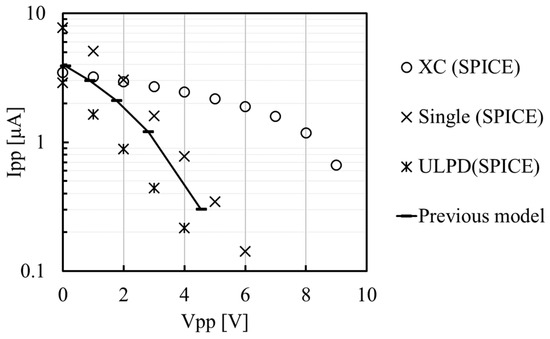
To directly take a look at differences in Ro among SD–CP, ULPD–CP, and XC–CP, SPICE simulation was conducted using the design parameters of a 65 nm CMOS, as shown in Table 1, resulting in Figure 3. Low-threshold-voltage transistors with a threshold voltage of about 0.3 V and with a minimum gate length of 60 nm were used. Surprisingly, the Ro of XC–CP was 3 times higher than those of SD–CP and ULPD–CP. As a result, the previous model [39,40] needs to be modified to predict high Ro for XC–CP.

Table 1.
Design parameters for Figure 3.
This paper proposes a circuit model of a cross-coupled CMOS AC–DC charge pump (XC–CP) operating in the subthreshold region. The aim is to improve the efficiency of designing XC–CPs with a variety of specifications, e.g., input and output voltages and AC input frequency. First, it is shown that the output resistance (Ro) of XC-CP is much higher than those of CPs with single diodes (SD–CP) and ultra-low-power diodes (ULPD–CP) as charge transfer switches (CTSs). Second, the reason behind the above feature of XC-CP, identified by a simple model, is that the gate-to-source voltages of CTS MOSFETs are independent of the output voltage of the CP. Third, the high but finite Ro of XC–CP is explainable with a more accurate model that includes the dependence of the saturation current of MOSFETs operating at a subthreshold voltage on the drain-to-source voltage, which is a faction of the output voltage of CP. The model is in good agreement with measured and simulated results of XC–, SD–, and ULPD–CPs fabricated in a 250 nm CMOS. Table 2 summarizes the abbreviations of the charge pumps discussed in this paper.

Table 2.
Abbreviations of the charge pumps discussed in this paper.
This paper is composed of the following sections. Section 2 overviews modeling of XC–CP [42,43] and shows the characteristics and schematics of the rectifiers composing each stage to be optimized. Section 3 presents the fabricated circuits and measurement results. Section 4 summarizes this research.
2. Modeling of Cross-Coupled CMOS AC–DC Charge Pump (XC–CP) Operating in Subthreshold Region
This section starts with a review of the previous AC–DC CP model [39,40], and proposes a new one for XC–CP operating in the subthreshold region. Table 3 summarizes the circuit parameters of the XC–CP.

Table 3.
Definition of design parameters.
2.1. Previous Model of AC–DC CP [39,40]
Figure 4a illustrates a sub-circuit of XC–CP to define the nodal voltages Vn and Vn+1. CLK and CLKB have a voltage amplitude of Vdd/2. Figure 4b shows the waveform of Vn and Vn+1.
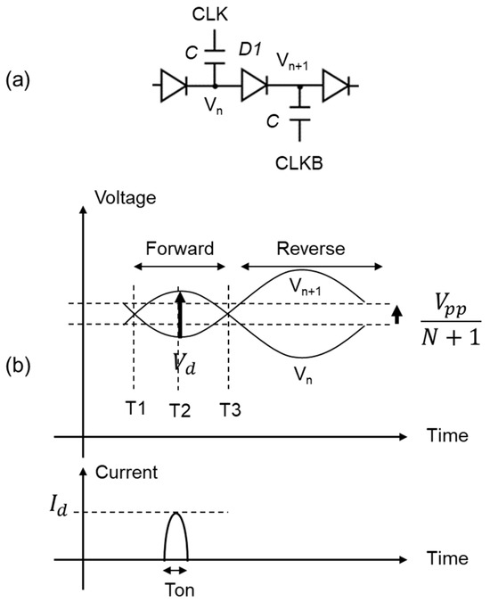
Figure 4.
Nodal voltages Vn and Vn+1 of neighboring stages (a) and their waveforms (b).
The charge transfer switch (CTS) or rectifying diode D1 operates a forward-bias regime between T1 and T3 and a reverse-bias one after T3. The peak forward voltage appears around the middle of the time period between T1 and T3, namely T2. V1 and V2 at T2 can be expressed as Vdd/2 − Ipp/fC and Vdd/2 + Ipp/fC + Vpp/(N + 1), respectively, where Vdd/2 is the clock amplitude of each of CLK and CLKB when the top plate parasitic capacitance is ignored for simplicity, Ipp is the output current, Ipp/fC is a voltage shift due to the amount of transferred charges Ipp/f in steady state, and Vpp/(N + 1) is the DC offset between the next-neighbor capacitor nodes. As a result, the voltage difference at the peak points of Vn and Vn+1 at T2 (Vd), is given by (1).
When the CTS MOSFET operates under the subthreshold region, the drain-to-source current Id is expressed by (2), where IS is the saturation current, Vgs the gate-to-source voltage, and VT is the effective thermal voltage.
with a conduction angle γ defined by Ton/Tc, i.e., (3), the average output current Ipp can be expressed by (4).
When Vgs is equal to Vd as in a single-MOSFET CTS, from (1), (2), and (4), one can determine the Vpp–Ipp relationship (5).
The “Previous model” in Figure 3 is given by (5). One can numerically calculate Vpp with a certain input value to Ipp.
2.2. Proposed Model of XC–CP
Figure 5a illustrates two next-neighbor stages of XC–CP. Because each stage has two capacitors, the capacitance of each capacitor is designed to be C/2 so that the total capacitance per stage is the same as the other CPs. The peak voltage difference Vd between the next-neighbor capacitors is the sum of the Vds of PMOSFET and NMOSFET, i.e., 2Vds. Figure 5b shows Vgs and Vd at the peak points. When the stage in the right half of Figure 5a is the second stage, V2D and V2U are given by −Vdd/2 + Ipp/fC + Vpp/(N + 1) and Vdd/2 − Ipp/fC + Vpp/(N + 1), respectively.
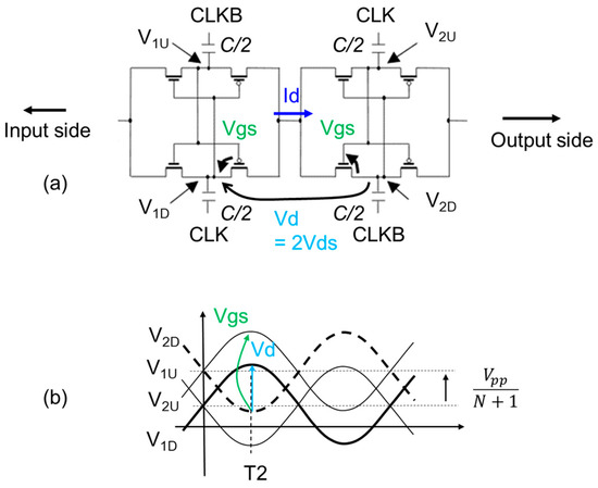
Figure 5.
Sub-circuit of XC–CP (a) and waveform of nodal voltages (b).
Thus, Vgs = V2U − V2D is given by (6).
Vd is given by (1) as well as SD–CP. Assuming NMOSFET has a drain-to-source current as large as PMOSFET does, the peak current from one capacitor to the next is given by (7).
Charge transfer occurs in every half cycle, resulting in (8).
From Vd = 2Vds and (6)–(8), a subthreshold XC–CP model is given by (9).
When , (9) is reduced to be (10). Because it has no Vpp term, this indicates that a subthreshold XC–CP is a current source with infinite output resistance. This fact is derived from (6), which has no dependency on Vpp.
2.3. More Accurate Model with Finite Output Resistance
Even though (10) can express high output resistance, it needs modification to have finite output resistance rather than infinite. Figure 6a shows the Ids − Vgs of an NMOSFET in a 250 nm CMOS, which suggests that Is has dependency on Vds, namely drain-induced barrier lowering. Hereinafter, low-threshold-voltage 5 V CMOS transistors with threshold voltages of about 0.3 V for NFET and about −0.3 V for PFET and with a minimum channel length of 0.25 μm were used. Based on the data of Figure 6a, Is − Vds is plotted in Figure 6b. The curve fits well with IS = 18.4 1010.7 Vds in nA.
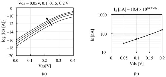
Figure 6.
Ids − Vgs (a) and extracted IS − Vds (b) of an NMOSFET in 250 nm CMOS.
Assuming the Is − Vds curve can be generally described by (9)–(11) can be revised to obtain (12) and (13), respectively.
Figure 7 compares Vpp − Ipp between SPICE and Models (10), (12), and (13) at Vdd = 200 mV when XC–CP is designed with the parameters in Table 4. Because Model (10) does not include Vpp, the curve is a line in parallel with the horizontal axis, meaning an infinite Ro. Both Models (12) and (13) have a Vpp term, and they show a finite Ro. Model (13) has a stronger function of Vpp than Model (12). Because of the performance limitation of the lab’s measuring instruments, the clock frequency was assumed to be 1 MHz. Also, in order to measure output power below 1 μW, the number of stages was determined to be 24. The three CPs were fabricated with these design parameters, and will be discussed in Section 3. Even though the short-circuit current at Vpp = 0 V had discrepancies when compared with the SPICE result, the output resistance of Model (13) was in better agreement with SPICE than that of Model (12).
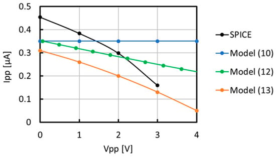
Figure 7.
Comparison of Vpp − Ipp between SPICE and Models (10), (12), and (13).
3. Validation of the Proposed Model
XC–CP, SD–CP, and ULPD–CP were designed in a 250 nm CMOS with the parameters shown in Table 4. Figure 8, Figure 9 and Figure 10, respectively, show simulated waveforms at 12th and 13th stages when Vdd is 400 mV and Vpp is 3.0 V. Note that V3 and the N- and P-well voltages of XC–CP in Figure 9, and V2 and V4 and the N- and P-well voltages of ULPD–CP in Figure 10, are much more stable than V1–V3 of SD–CP, as shown in Figure 8. That is because the ON-resistance of the two pass gates connected in series was designed to be about the same. Ideally, those nodal voltages become the averaged value of the nodal voltages of the two next-neighbor capacitors. This contributes to the power conversion efficiency of XC and ULPD CPs. The reduction in the voltage swing of the N-well potential results in a reduction in power loss. I1 and I2 of ULPD–CP become negative in the cycle time, but this is due to the AC current to the gate of the CTS transistors, not the actual leakage current.
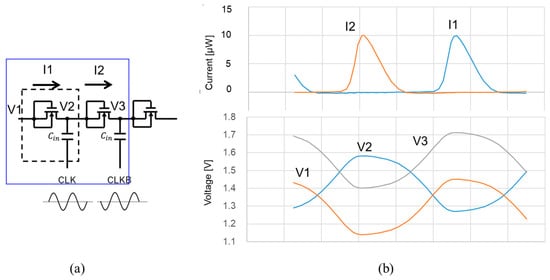
Figure 8.
The 12th and 13th stages of SD–CP (a) and their waveforms (b).
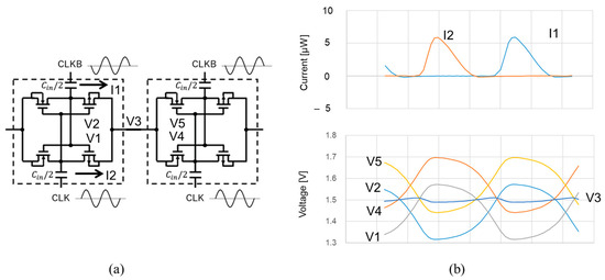
Figure 9.
The 12th and 13th stages of XC–CP (a) and their waveforms (b).
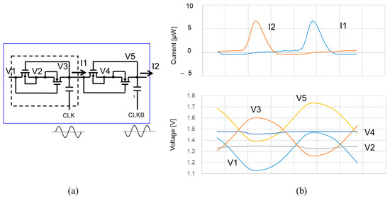
Figure 10.
The 12th and 13th stages of ULPD–CP (a) and their waveforms (b).
XC–CP, SD–CP, and ULPD–CP were fabricated in a 250 nm CMOS to validate the proposed model. Figure 11, Figure 12 and Figure 13, respectively illustrate the layout design for those three CPs.
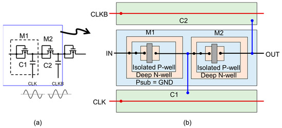
Figure 11.
Layout unit of SD–CP (a) and its layout design (b).
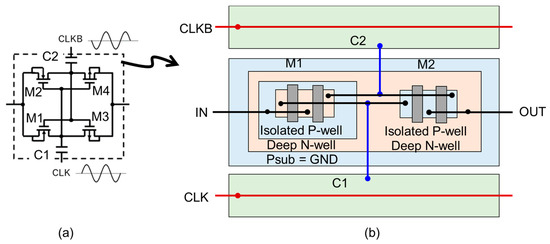
Figure 12.
Layout unit of XC–CP (a) and its layout design (b).
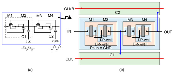
Figure 13.
Layout unit of ULPD–CP (a) and its layout design (b).
NMOSFETs were formed in a triple well to isolate their P-well from the P-substrate. The deep N-well of the NMOSFET is shared with the N-well for PMOSFET to minimize the parasitic capacitance for XC and ULPD CPs. To route wires for CLK and CLKB with minimal length, two adjacent stages are laid out by placing two capacitors at the top and bottom of the cell. The CTS is placed in the middle. The cell width is determined by the CTS and the cell height is determined by the two caps and the CTS.
Figure 14 shows a die photo. Each CP has 24 stages with a stage capacitor of 10 pF. Because of differences in the CTS size of the three CPs, XC, ULPD and SD, the CPs have overall sizes of 0.48 mm2, 0.49 mm2, and 0.44 mm2, respectively.
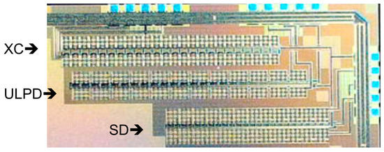
Figure 14.
Die photo.
Figure 15 shows the measured waveforms of the three CPs with a Vdd of 200 mV, f of 1 MHz, and a load resistance of 10 MΩ. The ripple voltages were below 6 mV with a filtering capacitance of 22 pF. Table 5 summarizes their DC values.
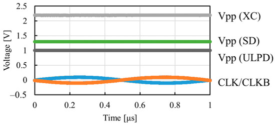
Figure 15.
Measured waveform with Vdd of 200 mV and f of 1 MHz.

Table 5.
Comparison of Vpp between SPICE and measured results in case of Vdd of 200 mV and f of 1 MHz.
Vpp was measured with various Vdd and load resistance values. Figure 16 compares the Vpp–Ipp curves between XC, ULPD, and SD with the SPICE, measurement, and model results. Hereinafter, the models for XC and SD indicate (13) and (5), respectively.
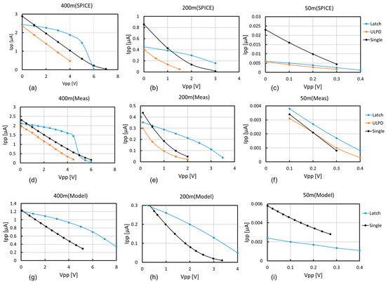
Figure 16.
Vpp–Ipp characteristics: SPICE results with Vdd of 400 mV (a), 200 mV (b), and 50 mV (c); measured results with Vdd of 400 mV (d), 200 mV (e), and 50 mV (f); models with Vdd of 400 mV (g), 200 mV (h), and 50 mV (i).
Figure 16a–c show the comparison of Vpp–Ipp curves given by SPICE simulation between XC, ULPD, and SD at Vdd values of 400 mV in Figure 16a, 200 mV in Figure 16b, and 50 mV in Figure 16c. At a Vdd of 400 mV or 200 mV, “Latch” or XC–CP had the highest Ro in a lower Vpp range, but Ipp suddenly collapsed at a certain Vpp. The reason for this behavior has not been identified in this work, and will be determined in research. An Isc of SC was the highest among the three CPs at Vdd values of 400 mV, 200 mV, and 50 mV. At a Vdd of 50 mV, the Ipp of XC is as low as that of ULPD. At such a low Vdd, the Vds of each CTS transistor may play a main role. The Vds of each CTS transistor in XC and ULPD is half of that in SD. When Vds goes below VT, (7) indicates that Ids is reduced as Vds decreases.
Figure 16d–f show a comparison of Vpp–Ipp curves given by measurement between XC, ULPD, and SD at Vdd values of 400 mV in Figure 16d, 200 mV in Figure 16e, and 50 mV in Figure 16f. The Vpp–Ipp characteristics at a Vdd of 400 mV or 200 mV between XC, ULPD, and SD were very similar to those of the SPICE results. Unlike the SPICE results, the Ipp values of the three CPs were about the same at the Vdd of 50 mV.
Figure 16g–i show a comparison of the Vpp–Ipp curves given by the models between XC and SD at Vdd values of 400 mV in Figure 16g, 200 mV in Figure 16h, and 50 mV in Figure 16i. The Ipp of XC was larger than SD when Vdd was 400 mV or 200 mV, whereas the Ipp of XC was smaller than SD when Vdd was 50 mV. These trends were similar to the SPICE results.
Figure 17 compares Vpp–Ipp curves between the SPICE, measurement, and model results. Figure 17a–c show a comparison of the Vpp–Ipp curves of XC–CP at Vdd values of 400 mV in Figure 17a, 200 mV in Figure 17b, and 50 mV in Figure 17c. The proposed model (13) was in good agreement with the SPICE and measured results within a factor of 3 in the swept ranges of Vpp and Vdd. The model did not succeed in showing sudden collapse at a certain Vpp with a Vdd of 400 mV. Note that the breakdown voltage of the PN junction between the P-substrate and N-well was higher than 9 V. This means that the sudden collapse occurs due to unknown phenomena in CPs, which should be identified in future work. Figure 17d–f show a comparison of the Vpp–Ipp curves of ULPD–CP at Vdd values of 400 mV in Figure 17d, 200 mV in Figure 17e, and 50 mV in Figure 17f. The SPICE and measured results were well matched in terms of the open-circuit voltage and within a discrepancy of 20% in terms of Ro. Figure 17g–i show a comparison of the Vpp–Ipp curves of SD–CP at Vdd values of 400 mV in Figure 17g, 200 mV in Figure 17h, and 50 mV in Figure 17i. Ro had discrepancies when compared with SPICE and measured results by a factor of two at a Vdd of 400 mV and was in good agreement with the measured results at Vdd values of 200 mV and 50 mV. The discrepancy in Ro between the SPICE and measured results increases as Vdd decreases in comparison with XC and ULPD. Discrepancies in the models against the measured and SPICE results were larger at a Vdd of 400 mV than at a Vdd of 200 mV. One possible reason for that is that the transistors of CTS enter into strong inversion at 400 mV, whereas they operate in weak inversion at 200 mV.
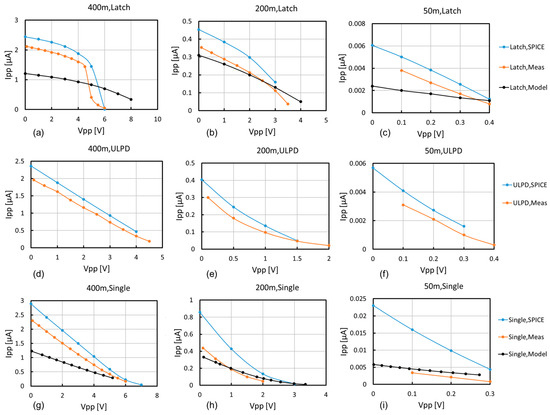
Figure 17.
Vpp–Ipp characteristics: XC–CP (latch) with Vdd values of 400 mV (a), 200 mV (b), and 50 mV (c); ULPD–CP with Vdd values of 400 mV (d), 200 mV (e), and 50 mV (f); SD–CP (Single) with Vdd values of 400 mV (g), 200 mV (h), and 50 mV (i).
Figure 18a–c compare the Ro in Figure 18a, Isc in Figure 18b, and Voc in Figure 18c of XC–CP between the SPICE, measured, and Model (13) results under the three conditions of (Vdd, Vpp) = (400 mV, 2.5 V), (200 mV, 1.0 V), and (50 mV, 0.2 V). The Voc of the model was closer to that of the SPICE and measured results than the Ro and Isc of the model were. This means that the discrepancy in the Ro of the model from the SPICE and measured results is as large as that in Isc. Figure 18d–f compare the Ro in Figure 18d, Isc in Figure 18e, and Voc in Figure 18f of SD–CP between the SPICE, measured, and Model (5) results under the three conditions of (Vdd, Vpp) = (400 mV, 2.5 V), (200 mV, 1.0 V), and (50 mV, 0.2 V). Like XC–CP, the Voc of the model was closer to that of the SPICE and measured results than the Ro and Isc of the model were.
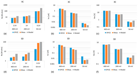
Figure 18.
Ro (a), Isc (b), and Voc (c) of XC–CP, and Ro (d), Isc (e), and Voc (f) of SD–CP between SPICE, measured and Model (13) results under three conditions of (Vdd, Vpp) = (400 mV, 2.5 V), (200 mV, 1.0 V), and (50 mV, 0.2 V).
Figure 19a–c compare Ro in Figure 19a, Isc in Figure 19b, and Voc in Figure 19c of XC–CP normalized by those of SD–CP between the SPICE, measured, and model results under the three conditions of (Vdd, Vpp) = (400 mV, 2.5 V), (200 mV, 1.0 V), and (50 mV, 0.2 V). From Figure 19a, except for the measured result at (Vdd, Vpp) = (50 mV, 0.2 V), the Ro of XC–CP was larger than that of SD–CP by a factor of 2.5 or more. When the condition of (Vdd, Vpp) moved from (400 mV, 2.5 V) to (200 mV, 1.0 V) and from (200 mV, 1.0 V) to (50 mV, 0.2 V), the Ro ratio increased with SPICE, whereas it did not with the measured and model results, except for the measured result from (200 mV, 1.0 V) to (50 mV, 0.2 V). Figure 19b shows that the Isc ratio decreased with the SPICE and model results, whereas it did not with the measured results. Figure 19c shows that the Voc ratios were in good agreement between the SPICE, measured, and model results in these three conditions even though the Ro ratio and the Isc ratio had different tendencies in the operation condition.

Figure 19.
Comparison of Ro (a), Isc (b), and Voc (c) of XC–CP normalized by those of SD–CP between SPICE, measured, and model results under the three conditions of (Vdd, Vpp) = (400 mV, 2.5 V), (200 mV, 1.0 V), and (50 mV, 0.2 V).
4. Conclusions
In this paper, a circuit model of AC–DC charge pumps with a subthreshold operation cross-coupled CMOS as a charge transfer switch (CTS), namely XC–CP, was developed for circuit designers to use the model for determining the initial condition for SPICE simulation. It was observed that XC–CP had much higher output resistance than charge pumps with single NMOSFETs as CTS, namely SD–CP. The reason is that the gate-to-source voltage of the MOSFETs in XC–CP does not depend on the output voltage unlike SD–CP and charge pumps with ultra-low-power diodes (ULPDs). Very high but finite output resistance results from the weak but finite dependence of the drain-to-source voltage on the subthreshold current through drain-induced barrier lowering. In both the SPICE simulation and measured results, the output current of XC–CP collapses at a certain output voltage. The developed model (13) does not predict this behavior. Further research is required to identify what leads to such behavior. To validate the proposed model, XC-, SD-, and ULPD–CPs were fabricated in a 250 nm CMOS. The output resistance predicted by the model was in good agreement with the SPICE and measured results within a factor of two at Vdd values of 400 mV, 200 mV, and 50 mV.
Author Contributions
Conceptualization, T.T.; methodology, R.K. and T.T.; software, R.K.; validation, R.K. and T.T.; formal analysis, R.K. and T.T.; investigation, R.K. and T.T.; writing—original draft preparation, R.K.; writing—review and editing, T.T. All authors have read and agreed to the published version of the manuscript.
Funding
This research received no external funding.
Data Availability Statement
Data are contained within the article.
Conflicts of Interest
The authors declare no conflict of interest.
References
- Umeda, T.; Yoshida, H.; Sekine, S.; Fujita, Y.; Suzuki, T.; Otaka, S. A 950-MHz Rectifier Circuit for Sensor Network Tags With 10-m Distance. IEEE J. Solid-State Circuits 2006, 41, 35–41. [Google Scholar] [CrossRef]
- Shetty, D.; Steffan, C.; Bösch, W.; Grosinger, J. Sub-GHz RF Energy Harvester including a Small Loop Antenna. In Proceedings of the 2022 IEEE Asian Solid-State Circuits Conference (A-SSCC), Taipei, Taiwan, 6–9 November 2022; pp. 1–3. [Google Scholar] [CrossRef]
- Hashimoto, T.; Nekozuka, H.; Toeda, Y.; Otani, M.; Fukuoka, Y.; Tanzawa, T. A− 31.7 dBm Sensitivity 0.011 mm2 CMOS On-Chip Rectifier for Microwave Wireless Power Transfer. Electronics 2023, 12, 1400. [Google Scholar] [CrossRef]
- Brown, W.C. The history of power transmission by radio waves. IEEE Trans. Microw. Theory Tech. 1984, 32, 1230–1242. [Google Scholar] [CrossRef]
- Jabbar, H.; Song, Y.S.; Jeong, T.T. RF energy harvesting system and circuits for charging of mobile devices. IEEE Trans. Consum. Electron. 2010, 56, 247–253. [Google Scholar] [CrossRef]
- Valenta, C.R.; Durgin, G.D. Harvesting wireless power: Survey of energy-harvester conversion efficiency in far-field, wireless power transfer systems. IEEE Microw. Mag. 2014, 15, 108–120. [Google Scholar]
- Yamazaki, Y.; Tsuchiaki, M.; Tanzawa, T. A Design Window for Device Parameters of Rectifying Diodes in 2.4 GHz Micro-watt RF Energy Harvesting. In Proceedings of the 2019 IEEE Asia-Pacific Microwave Conference (APMC), Singapore, 10–13 December 2019; pp. 135–137. [Google Scholar] [CrossRef]
- McSpadden, J.O.; Mankins, J.C. Space solar power programs and microwave wireless power transmission technology. IEEE Microw. Mag. 2002, 3, 46–57. [Google Scholar] [CrossRef]
- Strassner, B.; Chang, K. Microwave power transmission: Historical milestones and system components. Proc. IEEE 2013, 101, 1379–1396. [Google Scholar] [CrossRef]
- Ladan, S.; Guntupalli, A.B.; Wu, K. A high-efficiency 24 GHz rectenna development towards millimeter-wave energy harvesting and wireless power transmission. IEEE Trans. Circuits Syst. I Regul. Pap. 2014, 61, 3358–3366. [Google Scholar] [CrossRef]
- Kamada, H.; Yang, B.; Shao, W.; Shinohara, N.; Mitani, T. Application of Partially Driven Array Antenna to 28 GHz Near-Field WPT. In Proceedings of the 2022 Asia-Pacific Microwave Conference (APMC), Yokohama, Japan, 29 November–2 December 2022; IEEE: Piscataway Township, NJ, USA, 2022; pp. 255–257. [Google Scholar]
- Lee, H.M.; Ghovanloo, M. Fully integrated power-efficient AC-to-DC converter design in inductively-powered biomedical applications. In Proceedings of the 2011 IEEE Custom Integrated Circuits Conference (CICC), San Jose, CA, USA, 19–21 September 2011; IEEE: Piscataway Township, NJ, USA, 2011; pp. 1–8. [Google Scholar]
- Hashemi, S.S.; Sawan, M.; Savaria, Y. A high-efficiency low-voltage CMOS rectifier for harvesting energy in implantable devices. IEEE Trans. Biomed. Circuits Syst. 2012, 6, 326–335. [Google Scholar] [CrossRef]
- Li, X.; Tsui, C.Y.; Ki, W.H. A 13.56 MHz wireless power transfer system with reconfigurable resonant regulating rectifier and wireless power control for implantable medical devices. IEEE J. Solid-State Circuits 2015, 50, 978–989. [Google Scholar] [CrossRef]
- Noh, K.; Amanor-Boadu, J.; Zhang, M.; Sánchez-Sinencio, E. A 13.56-MHz CMOS active rectifier with a voltage mode switched-offset comparator for implantable medical devices. IEEE Trans. Very Large Scale Integr. (VLSI) Syst. 2018, 26, 2050–2060. [Google Scholar] [CrossRef]
- Ballo, A.; Bottaro, M.; Grasso, A.D. A review of power management integrated circuits for ultrasound-based energy harvesting in implantable medical devices. Appl. Sci. 2021, 11, 2487. [Google Scholar] [CrossRef]
- Beeby, S.P.; Tudor, M.J.; White, N.M. Energy harvesting vibration sources for microsystems applications. Meas. Sci. Technol. 2006, 17, R175. [Google Scholar] [CrossRef]
- Rahimi, A.; Zorlu, O.; Külah, H.; Muhtaroglu, A. An interface circuit prototype for a vibration-based electromagnetic energy harvester. In Proceedings of the 2010 International Conference on Energy Aware Computing, Cairo, Egypt, 16–18 December 2010; Institute of Electrical and Electronics Engineers (IEEE): Piscataway, NJ, USA; pp. 1–4. [Google Scholar]
- Maurath, D.; Becker, P.F.; Spreemann, D.; Manoli, Y. Efficient Energy Harvesting with Electromagnetic Energy Transducers Using Active Low-Voltage Rectification and Maximum Power Point Tracking. IEEE J. Solid-State Circuits 2012, 47, 1369–1380. [Google Scholar] [CrossRef]
- Kawauchi, H.; Tanzawa, T. A fully integrated clocked AC-DC charge pump for mignetostrictive vibration energy harvesting. Electronics 2020, 9, 2194. [Google Scholar] [CrossRef]
- Dickson, J.F. On-chip high-voltage generation in MNOS integrated circuits using an improved voltage multiplier technique. IEEE J. Solid-State Circuits 1976, SSC-11, 374–378. [Google Scholar] [CrossRef]
- Oh, S.; Wentzloff, D.D. A− 32dBm sensitivity RF power harvester in 130nm CMOS. In Proceedings of the 2012 IEEE Radio Frequency Integrated Circuits Symposium, Montreal, QC, Canada, 17–19 June 2012; IEEE: Piscataway Township, NJ, USA, 2012. [Google Scholar]
- Shameli, A.; Safarian, A.; Rofougaran, A.; Rofougaran, M.; De Flaviis, F. Power harvester design for passive UHF RFID tag using a voltage boosting technique. IEEE Trans. Microw. Theory Tech. 2007, 55, 1089–1097. [Google Scholar] [CrossRef]
- Levacq, D.; Liber, C.; Dessard, V.; Flandre, D. Composite ULP diode fabrication, modelling and applications in multi-Vth FDSOI CMOS technology. Solid-State Electron. 2004, 48, 1017–1025. [Google Scholar] [CrossRef]
- Szarka, G.D.; Stark, B.H.; Burrow, S.G. Review of power conditioning for kinetic energy harvesting systems. IEEE Trans. Power Electron. 2011, 27, 803–815. [Google Scholar] [CrossRef]
- Schmickl, S.; Faseth, T.; Pretl, H. An RF-energy harvester and IR-UWB transmitter for ultra-low-power battery-less biosensors. IEEE Trans. Circuits Syst. I Regul. Pap. 2020, 67, 1459–1468. [Google Scholar] [CrossRef]
- Gariboldi, R.; Pulvirenti, F. A 70 mΩ Intelligent High Side Switch with Full Diagnostics. IEEE J. Solid-State Circuits 1996, 31, 915–923. [Google Scholar] [CrossRef]
- Kotani, K.; Sasaki, A.; Ito, T. High-efficiency differential-drive CMOS rectifier for UHF RFIDs. IEEE J. Solid-State Circuits 2009, 44, 3011–3018. [Google Scholar] [CrossRef]
- Hwang, H.-W.; Chun, J.-H.; Kwon, K.-W. A low power cross-coupled charge pump with charge recycling scheme. In Proceedings of the 2009 3rd International Conference on Signals, Circuits and Systems (SCS), Medenine, Tunisia, 6–8 November 2009; IEEE: Piscataway Township, NJ, USA, 2009. [Google Scholar]
- Palumbo, G.; Pappalardo, D. Charge pump circuits: An overview on design strategies and topologies. IEEE Circuits Syst. Mag. 2010, 10, 31–45. [Google Scholar] [CrossRef]
- You, K.; Kim, H.; Kim, M.; Yang, Y. 900 MHz CMOS RF-to-DC converter using a cross-coupled charge pump for energy harvesting. In Proceedings of the 2011 IEEE International Symposium on Radio-Frequency Integration Technology, Beijing, China, 30 November–2 December 2011; IEEE: Piscataway Township, NJ, USA, 2011; pp. 149–152. [Google Scholar]
- Ballo, A.; Grasso, A.D.; Palumbo, G. A high-performance charge pump topology for very-low-voltage applications. IEEE Trans. Circuits Syst. II Express Briefs 2019, 67, 1304–1308. [Google Scholar] [CrossRef]
- Ballo, A.; Grasso, A.D.; Palumbo, G. A review of charge pump topologies for the power management of IoT nodes. Electronics 2019, 8, 480. [Google Scholar] [CrossRef]
- Ballo, A.; Grasso, A.D.; Palumbo, G. A subthreshold cross-coupled hybrid charge pump for 50-mV cold-start. IEEE Access 2020, 8, 188959–188969. [Google Scholar] [CrossRef]
- De Vita, G.; Iannacccone, G. Design criteria for the RF section of UHF and microwave passive RFID transponders. IEEE Trans. Microw. Theory Tech. 2005, 53, 2978–2990. [Google Scholar] [CrossRef]
- Yi, J.; Ki, W.-H.; Tsui, C.-Y. Analysis and design strategy of UHF micro-power CMOS rectifiers for micro-sensor and RFID applications. IEEE Trans. Circuits Syst. I Regul. Pap. 2007, 54, 153–166. [Google Scholar] [CrossRef]
- Barnett, R.E.; Liu, J.; Lazar, S. A RF to DC voltage conversion model for multi-stage rectifiers in UHF RFID transponders. IEEE J. Solid-State Circuits 2009, 44, 354–370. [Google Scholar] [CrossRef]
- Cardoso, A.J.; Montoro, C.G.; Schneider, M.C. Design of very low voltage CMOS rectifier circuits. In Proceedings of the IEEE Circuits and Systems for Medical and Environmental Applications Workshop (CASME), Merida, Mexico, 13–15 December 2010; pp. 1–4. [Google Scholar]
- Tanzawa, T. An analytical model of AC-DC voltage multipliers. In Proceedings of the 2014 21st IEEE International Conference on Electronics, Circuits and Systems (ICECS), Marseille, France, 7–10 December 2014; IEEE: Piscataway Township, NJ, USA, 2014. [Google Scholar]
- Tanzawa, T. An Analytical Model of AC-DC Charge Pump Voltage Multipliers. IEICE Trans. Electron. 2016, 99, 108–118. [Google Scholar] [CrossRef]
- Eid, M.H.; Rodriguez-Villegas, E. Analysis and design of cross-coupled charge pump for low power on chip applications. Microelectron. J. 2017, 66, 9–17. [Google Scholar] [CrossRef]
- Kotsubo, R.; Tanzawa, T. Modeling of subthreshold operation CMOS Latch-type RF-DC Charge Pump Circuits. In Proceedings of the Electronics Society Conference of IEICE, Virtual, 15–18 March 2022; Available online: http://hdl.handle.net/10297/00028678 (accessed on 17 November 2023).
- Kotsubo, R.; Tanzawa, T. The Origin of the Output Resistance in subthreshold Operation CMOS Latch-type RF-DC Charge Pump Circuits. In Proceedings of the Electronics Society Conference of IEICE, Nagoya, Japan, 6–9 September 2023; Available online: http://hdl.handle.net/10297/00029107 (accessed on 17 November 2023).
Disclaimer/Publisher’s Note: The statements, opinions and data contained in all publications are solely those of the individual author(s) and contributor(s) and not of MDPI and/or the editor(s). MDPI and/or the editor(s) disclaim responsibility for any injury to people or property resulting from any ideas, methods, instructions or products referred to in the content. |
© 2023 by the authors. Licensee MDPI, Basel, Switzerland. This article is an open access article distributed under the terms and conditions of the Creative Commons Attribution (CC BY) license (https://creativecommons.org/licenses/by/4.0/).