Article

A Double-Edge-Triggered Digital LDO with Built-In Adaptive VCO Clock for Fast Transient Response and Low Power Consumption

School of Electronic Engineering, Xi’an University of Posts & Telecommunications, Xi’an 710121, China
*
Author to whom correspondence should be addressed.
Electronics 2023, 12(19), 4100; https://doi.org/10.3390/electronics12194100
Submission received: 19 August 2023 / Revised: 21 September 2023 / Accepted: 28 September 2023 / Published: 29 September 2023

Abstract

:
A double-edge-triggered digital low dropout regulator (DLDO) is proposed with a built-in adaptive voltage-controlled oscillator (VCO) clock (AVC) for a system-on-chip (SoC) application. To achieve a fast transient response, the main comparator generates the comparison result at the rising edge of the AVC, and this result is sampled by the coarse or fine bidirectional shifter register at the falling edge of the AVC. Furthermore, the clock frequency can be boosted from 8 MHz at the steady state to 50 MHz by the AVC when the output current suffers from a sudden change, and it can also be adjusted in real-time according to the output voltage, which avoids the oscillation phenomenon and decreases the power consumption during the recovery process. To further lower the power consumption, the self-clock comparator replaces the conventional static comparator in the transient detector. The post-simulation results show that the proposed DLDO consumes a quiescent current of 95.13 μA in the steady state, and drives a maximum load current of 25 mA at the supply power of 0.6 V with an active area of 0.053-mm2 in a 180 nm CMOS process. When the load current jumps from 0.5 mA to 25 mA at the edge of 100 ps, the undershoot voltage and overshoot voltage are only 335 mV with the recovery time of 2.7 μs and 47.6 mV with the recovery time of 2.1 μs at the total on-chip capacitor of 50 pF, respectively, resulting in two competitive figures of merits (FoMs) than the previous works.

1. Introduction

In Internet of Things (IoT) and system-on-chip (SoC) application scenarios, energy-efficient fine-grained power management systems are indispensable for self-power wireless sensors due to the limited power capability of the supply and energy harvester. At high supply voltages (e.g., 1.2 V and above), analog low-dropout regulators (LDOs) can regulate a constant voltage for analog and RF modules due to their excellent noise performance and high PSRR characteristics, which maximize the performance and energy efficiency [1,2]. With CMOS process scaling, the intrinsic gain of the transistors is smaller, leading to an analog circuit accuracy reduction. Although the multistage operational transconductance amplifier improves the gain, it also introduces stability issues and considerable power consumption. In addition, in the near-threshold range (62 mV to 0.6 V), the analog LDO (ALDO) also fails to show excellent energy efficiency. Recently, the digital LDO (DLDO) features low voltage operation, process scalability, and other benefits associated with digital-oriented design, which has received the attention of many researchers [3].
Compared with the DLDO with the power PMOS transistors, the DLDO with the power NMOS transistor can provide additional current through their intrinsic loop (Vgs) to optimize the undershoot voltage and the response time during the output voltage recovery process. Nevertheless, this type of DLDO requires a charge pump circuit and the level shifter to ensure that the gate voltage of the power NMOS transistor is higher than the supply voltage [4]. This leads to extra area and power consumption in the level shifter, charge pump, and capacitance. The classic digital LDOs improve the clock frequency of the dynamic comparator and the bidirectional shift register (S/R) for a better transient response, but increase the static power Iq in the steady state [5]. Therefore, it is crucial to enhance the transient response while simultaneously reducing the power consumption.
There are various approaches to enhance the dynamic response of digital LDOs. One method is to use asynchronous clocking [6] or the self-clock technique [7] instead of the synchronous clock as the trigger method of the comparator and the S/R. However, asynchronous clocking can make the logic design more intricate and susceptible to voltage and temperature variations, which compromises the robustness of the system. Another strategy involves modifying the structure of the power PMOS transistor array, for instance, a binary-weighted PMOS capacitor array. Because the most significant bit PMOS transistor always offers the maximum current whether large or small jumps occur in the output voltage, this leads to the oscillation phenomenon and a long recovery time when a small output voltage change occurs [8]. Dual-loop regulation is an effective way to avoid the oscillation phenomenon by utilizing an extra transient detector (TD) to check the output changes. The coarse loop is used to quicken the output level recovery when the output exceeds the detection boundaries, and when the threshold level is not surpassed, the PMOS transistor in the fine loop is switched at each clock edge for high accuracy and current efficiency. However, the continuous-time (CT) comparator in the TD can increase the static power consumption of the digital LDO [9]. The analog-assisted (AA) technique uses a coupling capacitor CC with a resistance R1 that forms a high-pass filter to compensate the transient current to the gate of the PMOS transistor, which is a promising technology as there is no additional static power consumption [10]. However, the performance is degraded in the light-to-heavy load transient case because the transconductance of the PMOS transistors is too small to fully compensate for the load transient current. Fortunately, the light load current can reach about several hundred μA. The only fly in the ointment is that the transient response can be boosted at the expense of area (CC = 120 pF). Finally, the fifth technique is adaptive clocking, which selects the clock frequency of the comparator and the S/R. However, the glitch during the fast/slow clock switching process may affect the performance of the circuit [11].
To address the above-mentioned issues, the comparator and bidirectional S/R were controlled with different trigger methods without extra circuit assistance and robustness issues in our work. Specifically, the comparator obtains the quantization result at the rising edge, while the bidirectional S/R then samples and shifts this quantization result at the falling edge. As a result, the transient response can be enhanced because the PMOS array can adjust the output current in the current cycle. In other words, this trigger technology can relax the clock frequency at the steady state by 2×. In addition, a built-in adaptive voltage-controlled oscillator (VCO) clock (AVC) is proposed to reduce both the static and transient power consumption by adjusting the clock frequency of the comparator and bidirectional S/R in real-time according to the output voltage. When the output current change jumps from 0.5 mA to 25 mA within 100 ps, the clock frequency of the AVC is boosted from 8 MHz in the steady state to 50 MHz, which lowers the undershoot voltage and the recovery time in the undershoot case and overshoot case to 335 mV, 2.7 μs, and 2.1 μs. To boost the current efficiency, the self-clock comparator in the transient detector is employed. The post-simulation results show that the proposed DLDO can provide a load current from 0.5 mA to 25 mA and achieve a peak current efficiency of 99.6% at the supply voltage of 0.6 V with an active area of 0.053 mm2 in a standard 0.18 μm CMOS process, leading to the FoM1 and FoM2 of 2.654 ps and 0.13 pF, respectively.
The rest of this paper is organized as follows. Section 2 describes the architecture and working principle of the proposed DLDO. Section 3 demonstrates the circuit implementations and design considerations of each circuit module. Section 4 presents the simulation results and comparisons. Section 5 concludes this work.

2. Architecture and Working Principle

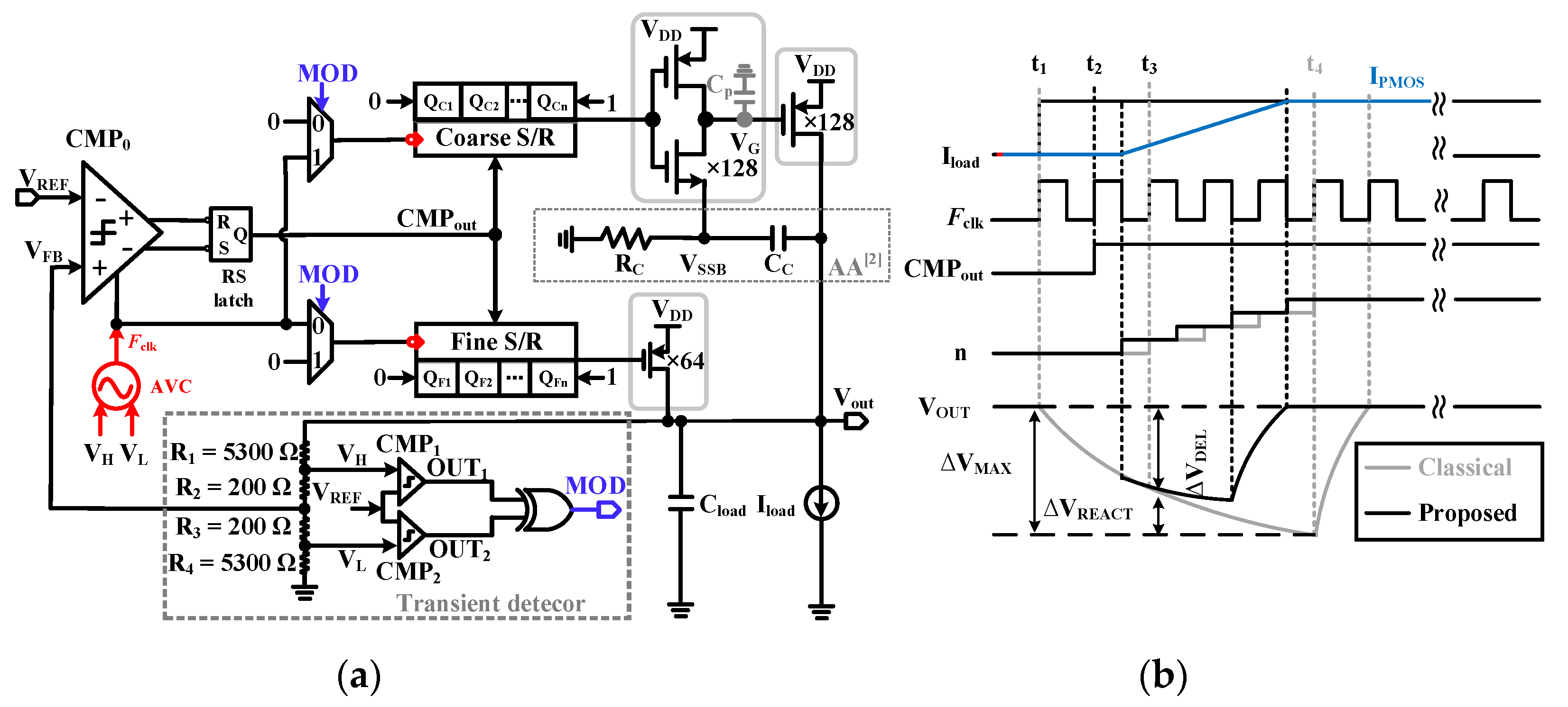
Figure 1a presents the overall architecture of the proposed DLDO with an AA loop from Ref. [4]. The proposed DLDO consists of the main comparator CMP0 with an RS latch, two selectors controlled by the MOD signal, the coarse and fine bidirectional S/R, the coarse and fine power PMOS transistor arrays, the AVC, and the TD.
To trade off the power and transient response, the PMOS array is divided by 128 coarse PMOS transistors with a size of 100 μm/0.18 μm and 64 fine PMOS transistors with a size of 10 μm/0.18 μm. The total size of the coarse PMOS array is mainly determined by the maximum load current, while the size of the unit for the fine PMOS transistor is decided by the minimum load current. Under the same maximum output current capability, as the bits of the coarse PMOS array increases, for example, 256 bits, the output current of every unit of the coarse PMOS transistor is halved, which not only increases the area of the coarse bidirectional SR, but also prolongs the recovery time. In contrast, with the decrease in the bit of the coarse PMOS array such as 64 bits, the transient current provided by every coarse PMOS transistor is increased by more than two times at a large undershoot in the output voltage since the source to drain voltage (Vsd) of every coarse PMOS transistor increases from 50 mV in the steady state to several hundred mV in the transient response. The simulation shows that the output current of every coarse PMOS transistor with a size of 400 μm/0.18 μm is 924 μA and 1.8 mA at the Vsd of 50 mV and 300 mV, which is much higher than the total current (828 μA) provided by the fine PMOS array. However, by doing this, the output suffers from the overshoot voltage after the undershoot voltage, which still prolongs the recovery time. More significantly, the proposed DLDO cannot switch from the coarse loop to the fine loop during the output recovery process. Furthermore, the RS latch can protect or temporarily store the main comparator result during the comparator reset phase.
It can be seen from Figure 1 that the gate voltage of the power PMOS transistors is determined by the coarse/fine loop bidirectional S/R and the AA loop. When the output current increases suddenly, the output voltage of the proposed DLDO decreases sharply, and the output voltage change is assumed as ΔVout. The AA loop has a faster response than the main loop of the DLDO, and thus the gate voltage can reduce CC·ΔVout/(CC + CP) immediately to lower the undershoot voltage, where CP is the parasitic gate capacitor of the power PMOS transistors. In the proposed work, the total size of the fine PMOS array is only 1/20 of that of the coarse PMOS array. Therefore, the undershoot voltage dominantly relies on the coarse PMOS array. Furthermore, even if the AA loop is employed in the fine PMOS array, the undershoot voltage cannot be optimized obviously because the parasitic capacitance of the fine PMOS array is contained and the gate voltage change of all PMOS transistors is reduced under the identical CC. Therefore, the AA loop is only used for the coarse PMOS array by trading off the undershoot voltage and gate voltage change of the power PMOS transistors.
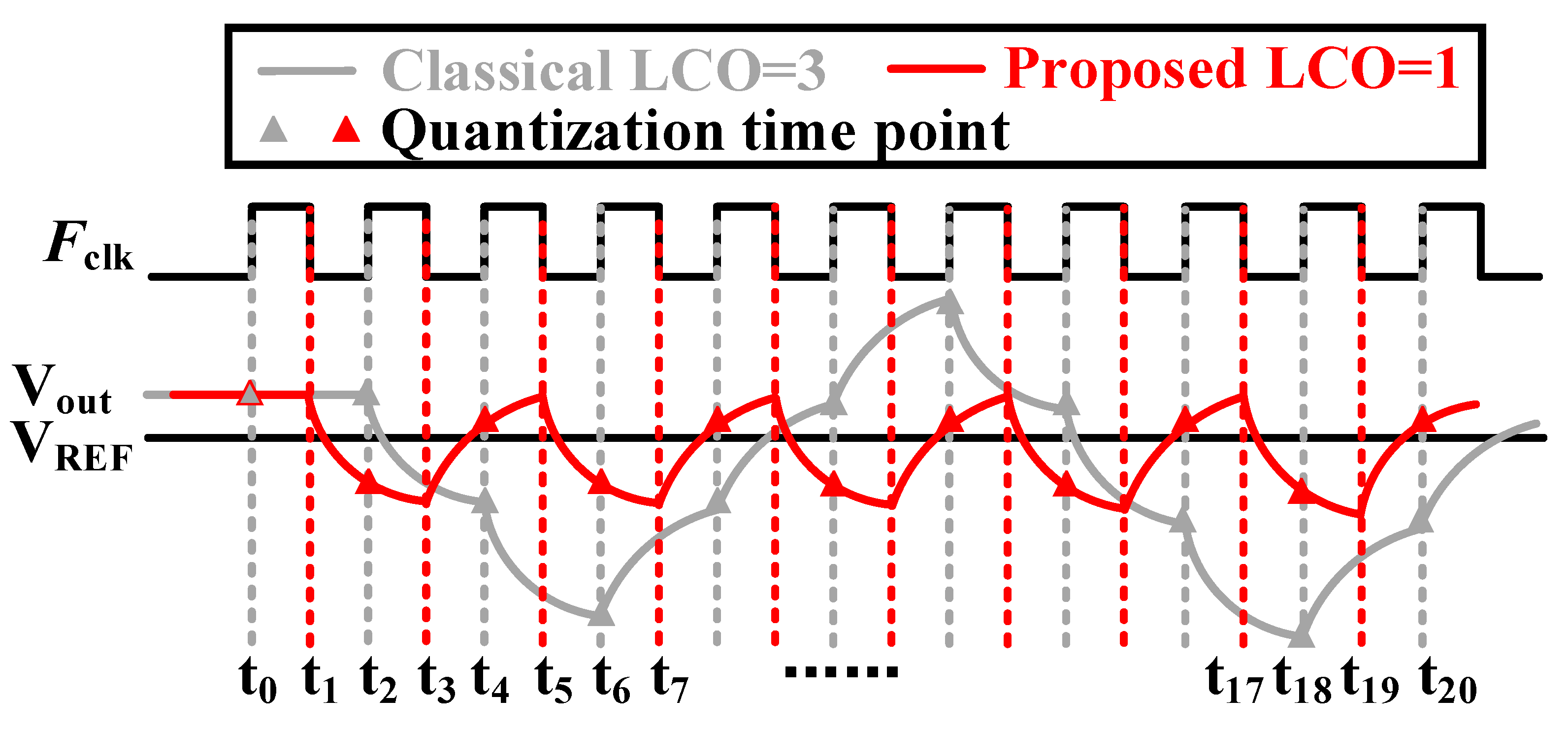
Figure 1b shows the transient response comparison between the classical DLDO [5] and the proposed DLDO. When the load current (Iload) steps up at t1 within a rapid edge time, the CMP0 and the SR latch hardly provide a correct comparison result (CMPout) due to the limited comparison time (1/(2·Fclk)). At t2, the CMPout turns to the high level at the rising edge of Fclk. Now, the coarse S/R is selected by the MOD because the VOUT exceeds the threshold boundary, unlike the S/R of the classical DLDO [5] and the conventional coarse-fine loop DLDO [9], which is triggered in the next cycle t3. The S/R in the proposed DLDO is triggered at the falling edge to turn on the power PMOS transistor to supplement the output current to reduce the ΔVDEL until the IPMOS is equal to Iload. In other words, the transient response can be enhanced by triggering the comparator CMP0 and the S/R at the rising and falling edge, respectively, without the clock frequency increment and any hardware cost.
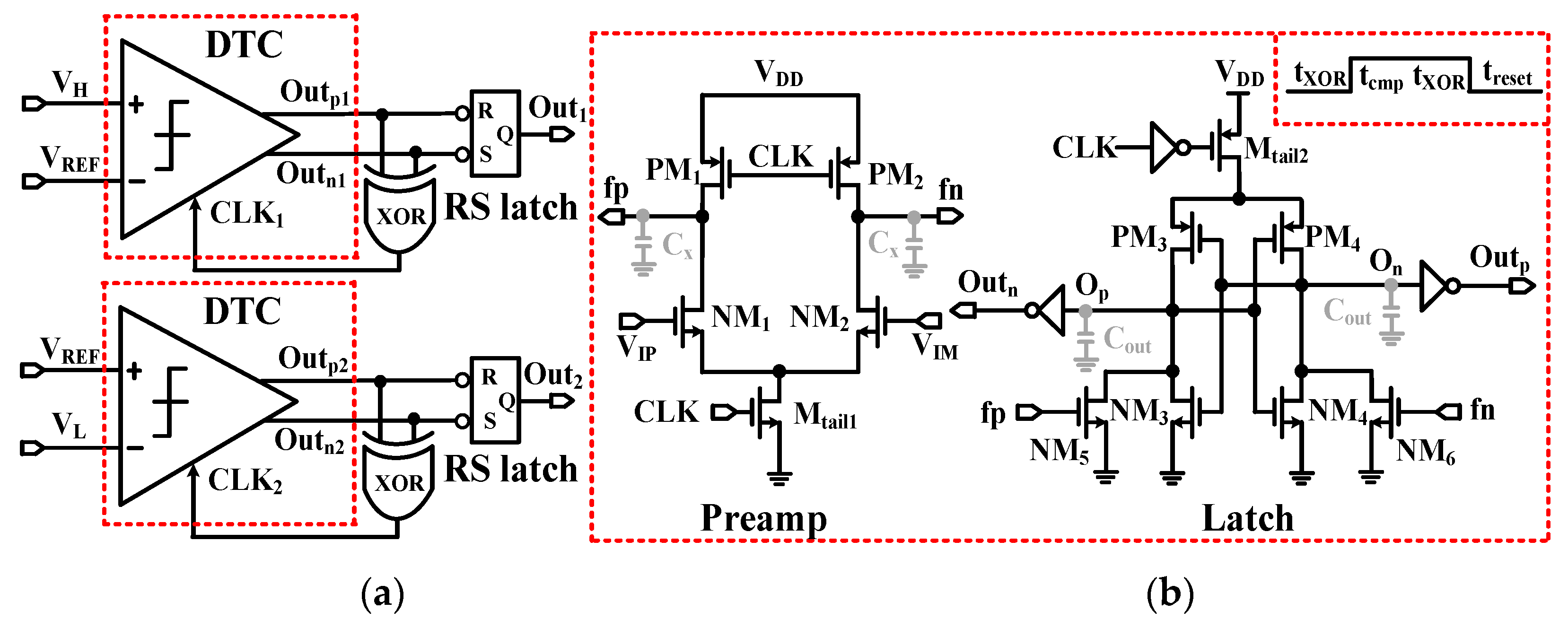
Unlike the conventional TD [12], the self-clocked comparators CMP1 and CMP2 replace two CT comparators to lower the power consumption, and the operation frequency of these two comparators is enhanced to 58 MHz to diminish the comparator’s delay effect on the DLDO at a supply voltage of 0.6 V. The four resistors R1, R2, R3, and R4 in the TD have resistance values of 5300 Ω, 200 Ω, 200 Ω, and 5300 Ω, respectively. Therefore, VH, VFB, and VL can be calculated as follows:
V H = R 2 + R 3 + R 4 R 1 + R 2 + R 3 + R 4 V out V FB = R 3 + R 4 R 1 + R 2 + R 3 + R 4 V out V L = R 4 R 1 + R 2 + R 3 + R 4 V out
According to Equation (1), even if there is a resistance mismatch, VH must be larger than VREF, while VL must be smaller than VREF. If the TD range is too small (2 mV), the proposed DLDO will jump from the fine loop to the coarse loop with a slight change in the output voltage. As a result, the output voltage will oscillate during output recovery due to multiple overshoots and undershoots, resulting in a long recovery time. If the TD range is too large (200 mV), it is difficult to switch the proposed DLDO from the fine loop to the coarse loop with a large jump in the output. As a consequence, this situation also leads to a long recovery time since the current provided by each PMOS transistor in the fine loop is small. In our design, the TD range was designed to be 20 mV by compromising the recovery time in the case of the large jump and the small jump in the output voltage. In addition, the VH and VL were designed for 285 mV and 265 mV, respectively, by the series resistor ladder instead of the voltage reference for the dynamic voltage scaling. The voltage reference operating in the subthreshold region or the 2T solution in [13] can dramatically reduce the static power consumption. However, the series resistor ladder was used in our work for two reasons. Firstly, VH, VL, and VFB vary with the supply voltage to achieve a fixed Vdrop. The voltage reference (2T solution) can only provide a fixed level under different PVT conditions, which shrinks the supply voltage range. Secondly, we assumed that a voltage reference with the value of 285 mV was designed with the nanowatt level power consumption. An external operational amplifier is still required to generate a voltage reference value of 265 mV, resulting in additional power consumption and increased circuit complexity. When the load current changes sharply, the overshoot voltage or undershoot voltage exceeds the threshold voltage VH or VL, and then the MOD outputs 1. The AVC generates a high-frequency clock. At the same time, the comparator and coarse bidirectional S/R, controlled by this high-frequency clock, can quickly recover the output voltage through a coarse PMOS array until VFB is recovered between the VH and VL levels. More importantly, because the clock frequency (Fclk) is controlled by the VH and VL associated with the output of the DLDO (Vout), it will decrease with the decrease in the undershoot voltage. Therefore, the oscillation at Vout can effectively be avoided during the signal recovery process. When the circuit output is at a steady state or when the overshoot voltage or undershoot voltage is small, MOD outputs 0, and the AVC produces a corresponding low-frequency clock to control the CMP0 and the fine-loop bidirectional SR for the output voltage recovery. Meanwhile, the coarse bidirectional SR is idle to lower the power consumption.

3. Design Results and Comparison

3.1. Dynamic Comparator Design

The self-clock comparators CMP1 and CMP2 in the TD shown in Figure 2 consist of a double-tail comparator (DTC), an XOR, and an SR latch. Assuming that the initial outputs Outp and Outn are at the low level at the reset state, the CLK becomes the high level after the delay of the XOR (tXOR), and then the comparator starts to compare the feedback signals (VH and VL) and VREF to generate the new results Outp and Outn after the delay of the comparator (tcmp). By performing an XOR for the new results Outp and Outn, the CLK becomes the low level after the tNOR, and the comparator can also be reset after the reset time of the comparator. Hence, the operation frequency of the self-clock comparator can be written as:
f clk = 1 / 2 t XOR + t reset + t cmp
Compared to the strong-arm comparator, the DTC is made up of the preamplifier stage (preamp) and the second latch stage, and the kickback noise can be isolated by the preamplifier stage in the low-voltage operation. The main comparator CMP0 is controlled by the AVC to enhance the transient response, while the comparators CMP1 and CMP2 are controlled by the clocks CLK1 and CLK2 separately for the output voltage detection in real-time. To analyze the delay of the comparator (tcmp), the operation process of the DTC is divided into three phases: the reset phase, the integrated phase, and the latch phase. The delay in the integrated phase (t0) and the latch phase (tlatch) of the comparator is the dominant factor. t0 represents the charging process to the load capacitor (Cout) until the first n-channel transistor (NM3/NM4) turns on. tlatch stands for the latching delay of two cross-coupled inverters (PM3, PM4, NM3, and NM4 transistors), which is from an initial output voltage difference V0 (The final state of the integral phase) to a voltage swing of Voutp − Voutn = VDD/2. The total delay (tcmp) of this comparator can be evaluated as follows [14]:
t cmp = t 0 + t latch = 2 V t h n m 5 , 6 C out I t a i l 2 + C out g m , i n v l n V D D / 2 Δ V 0 = 2 V t h n m 5 , 6 C out I t a i l 2 + C out g m , i n v l n V D D I t a i l 2 2 C X 8 g m n m 1 , 2 g m n m 5 , 6 C out V t h n m 5 , 6 2 Δ V i n
where CX is the output parasitic capacitor at the nodes fn and fp, gmnm1,2, gmnm5,6, and gm,inv are the transconductance of the NM1, NM2, NM5, and NM6 transistors, and the two cross-coupled inverters, Itail2 and Vthnm5,6 stand for the tail current of the Mtail2 transistor at the latch phase and the threshold voltage of the NM5 and NM6 transistors. It can be seen from Formula (3) that the delay of the comparator can be affected by the input level difference and the process corners.
Figure 2. (a) Schematic of the comparator with the self-clocked technology. (b) Schematic of the double-tail dynamic comparator.
Electronics 12 04100 g002
The effect of the offset voltage of the comparator on the proposed DLDO can be equivalent to the effect on the accuracy of the voltage reference (VREF). The offset voltage can be calculated as follows:
V os = V os ,   preamp + 1 A preamp V os ,   latch
where Vos, preamp and Vos, latch are the offset of the preamplifier stage and the second latch stage. Apreamp represents the gain of the preamplifier stage. Since the Vos, latch is damped by the preamplifier stage, the offset voltage of the dynamic comparator is dominated by that of the preamplifier stage and the Vos, preamp can be expressed as follows [15]:
V os , preamp = Δ V thNM 1 , 2 + V gs V th NM 1 , 2 2 Δ S N M 1 , 2 S N M 1 , 2 + Δ R N M 1 , 2 R N M 1 , 2
where ∆VthNM1,2, ∆SNM1,2, and ∆RNM1,2 indicate the threshold voltage mismatch, the parameter (μCOXW/L) mismatch of the NM1 and NM2 transistors, and the equivalent load mismatch at the nodes fp and fn, respectively. (Vgs-Vth)NM1,2 stands for the overdrive voltage of the NM1 and NM2 transistors. Therefore, the W/L of the input transistor NM1 and NM2 needs to be increased to suppress the offset voltage of the DTC. When the positive side of the comparator is increased linearly from 265 mV to 285 mV in 20 μs, and the negative side of the comparator is fixed at 275 mV, Figure 3 shows the 500-run Monte Carlo simulation of the offset voltage at the clock frequency of 8 MHz and 50 MHz. The type of Monte Carlo simulation is “process and mismatch”. The mean and standard deviation of the comparator’s offset voltage are independent of the clock frequency and are about 700 μV, which can match the theoretical calculation.

3.2. Built-In Adaptive VCO Clock

Figure 4a presents the schematic of the AVC, which is composed of the 11-stage inverter-based ring oscillator in Figure 4b, the pull-down controlled transistors (MN1-MN6), and the pull-up-controlled transistor (MP1-MP6). The working state of the AVC is decided by the TD. When the proposed DLDO is in the steady state (VH > VREF > VL), the outputs Out1 and Out2 of the self-clocked comparator CMP1 and CMP2 are high level, and the oscillation frequency of the AVC is determined by the pull-up current of 1.3 μA from the MP3 transistor and the pull-down current of 1.4 μA from the MN3 transistor. If the pull-up current is equal to the pull-down current in the steady state, the AVC will generate a clock with a duty cycle of 50%. Because the reset time (Tres) at the low level of the main comparator (CMP0) is independent of the input signal amplitude, it can be less than the quantization time (Tquan) at the high level to improve the operating frequency of the CMP0. That is to say, it is not necessary to design the clock duty ratio of 50% under the steady state. Because the pull-up current is less than the pull-down current, the pull-up time is greater than the pull-down time for every inverter in Figure 4b. The Tres at the low level and the Tquan at the high level can be calculated as follows:
T res = 6 t inv _ pu + 5 t inv _ pd T quan = 5 t inv _ pu + 6 t inv _ pd
It can be seen from Formula (6) that the reset time of the comparator is just less than the quantization time of the comparator.
This oscillation frequency of the AVC can be calculated as 8.13 MHz, which can match the simulation result (8 MHz). When the output (Vout) of the proposed DLDO encounters a large undershoot in the transient response (VH < VREF), the Out1 turns to the low level and the Out2 remains at the high level. The pull-down current from the current mirror (the MN1 and MN2 transistors) and the extra pull-up current from the MP2 transistor can boost the oscillation frequency of the AVC. Meanwhile, the pull-down current is controlled by the VL, and the larger the undershoot voltage, the higher the IMN2 current and oscillation frequency of the AVC. Similarly, when the overcharge voltage occurs (VL > VREF), the oscillation frequency of the AVC is also enhanced by the pull-up current from the MP4 transistor and the extra pull-down current from the MN4 transistor. Figure 4c summarizes the working state and the oscillation frequency of the AVC in different conditions of the DLDO. Figure 5a shows that the clock frequency of the AVC varies with the VL and VH. Fclk is only 8 MHz at the steady state; the Fclk can be boosted up to about 50 MHz at the transient response at a 0.6 V supply through the PSS simulation.
The clock frequency of the AVC at different temperatures and corners at the steady state and transient state is presented in Table 1. The slowest frequency and fastest clock frequency occur at the −40 ℃@ss corner and 85 ℃@ff corner. Furthermore, the clock frequency ratio between the steady state and the transient state is almost 1:6.25 at any process corner and temperature. Figure 5b shows the 500-run Monte Carlo simulation of the clock frequency at the steady state and transient state. The mean value and standard deviation of the clock frequency at the steady state are 8.21 MHz and 2.48 MHz, respectively, while those of the clock frequency at the undershoot case and overshoot case are nearly 52 MHz and 11.61 MHz, and 50.82 MHz and 13.12 MHz, respectively.

3.3. Loop Stability Analysis

Following a similar analysis presented in [4,10], the small signal model and the zero-pole distribution are demonstrated in Figure 6a and 6b, respectively. The bidirectional S/R acts as an ideal discrete-time integrator with a dc pole (p0) with the gain of KSR. The PMOS array outputs a constant current and provides a gain of KDC until the next negative clock edge, thus a zero-order hold (ZOH) is placed in front of the output stage, which is modeled by the load resistor (Rload) and the load capacitor (Cload). Hence, the second pole p2 and the third parasitic pole p3 are located at the output node Vout and the gate of the power transistor (VG), where Ron1 and Ron2 stand for the output resistance of the turn-on power transistors and the output resistance of the inverter in the coarse loop and the S/R in the fine loop at node VG. The p3 is far away from the unit gain-bandwidth product, which does not affect the loop stability. Furthermore, the AA loop in Figure 6b introduces a dc zero z0 and a pole pAA, and it does not work in the steady state of the DLDO. Therefore, the open-loop transfer function H(s)open_loop and closed-loop transfer function H(s)close-loop in the steady state can be expressed respectively as follows:
H s o p e n _ l o o p = e s T c l k / 2 K SR 1 1 z 1 1 e T c l k s K DC 1 + s / F l o a d = K forward z 1 1 e F l o a d / F c l k z e F l o a d / F c l k
H s c l o s e _ l o o p = H s o p e n _ l o o p 1 + H s o p e n _ l o o p = K forward 1 e F l o a d / F c l k z 1 z e F l o a d / F c l k + K forward 1 e F l o a d / F c l k
where the forward gain Kforward = KSR·KDC, and Fload and Fclk are the output pole frequency ((Ron1||Rload)·CLoad)−1 and the adaptive clock frequency, respectively. Unlike the analog LDO, the DLDO cannot directly reflect the zero-pole point position and the phase characteristics by the AC simulation. The DLDO judges the stability by the distribution of poles in the z plane. As analyzed in Equation (7), one pole is located on the unit circle, which is derived from the S/R. The other pole is determined by the Fload and Fclk together. The worst case of stability is at the light load due to a large output resistance. In the pre-simulation, the Fclk of the AVC was 8 MHz and the Fload was 36.4 MHz. In the post-simulation, the Fclk was reduced to 7.8 MHz, and the Fload was reduced to 35.8 MHz. Hence, the second pole was almost unchanged and hardly affected the stability. Based on the MATLAB model, under the condition of the constant sampling rate Fclk, with the decrease in the load current, the decrease in Fload makes the two poles (z = 1 and z = eFload/Fclk) closer in Figure 7a, and easily leads to the instability of the system because the phase margin (PM) is decreased from 84.8° to 45.1°, as shown in Figure 7b. The stability of the proposed DLDO benefits from the AVC technology because the clock frequency of Fclk can drop down to 8 MHz whether under a heavy or light load.

3.4. LCO Issues at the Steady State

The intrinsic quantization noise of the DLDO causes the output ripple at the steady state, which is also known as the limit cycle oscillation (LCO) phenomenon. Normally, the LCO period is 2M times the clock period (Tclk), where M is the mode of the LCO. In the classical DLDO, since the bidirectional S/R always samples the quantization result of the previous cycle in Figure 8, the response time of the power PMOS array has a period delay, resulting in the obvious voltage ripple in the conventional DLDO. With the double-edge-trigger method, the comparator performs quantization at a high level, and the S/R outputs and shifts the comparator result at the falling edge in the same cycle. Therefore, the proposed digital LDO can prompt the output timelier than the classical DLDO.
As shown in Figure 8, when Vout is slightly higher than the VREF in the steady state, the comparator performs quantization at t0, a single PMOS power transistor controlled by the fine bidirectional S/R can be switched off to reduce the output current at t1, and the output begins to be pulled down. If the settling time τ, decided by the output pole, is less than half of the sampling clock cycle (Tclk/2), the output voltage can be stable at the next quantization point t2. According to the comparator result, the PMOS array turns on a single PMOS transistor to provide the output current from the moment t3, and then the output voltage begins to be stretched to a level higher than VREF, like the moment t0. As depicted in Figure 8, the mode of the LCO can be reduced from 3 to 1. Compared with the auxiliary redundant PMOS power transistor in the feedforward path [16,17], the proposed LDO can reduce the LCO mode to 1 without adding any extra power consumption or design complexity.

4. Simulation Results and Comparisons

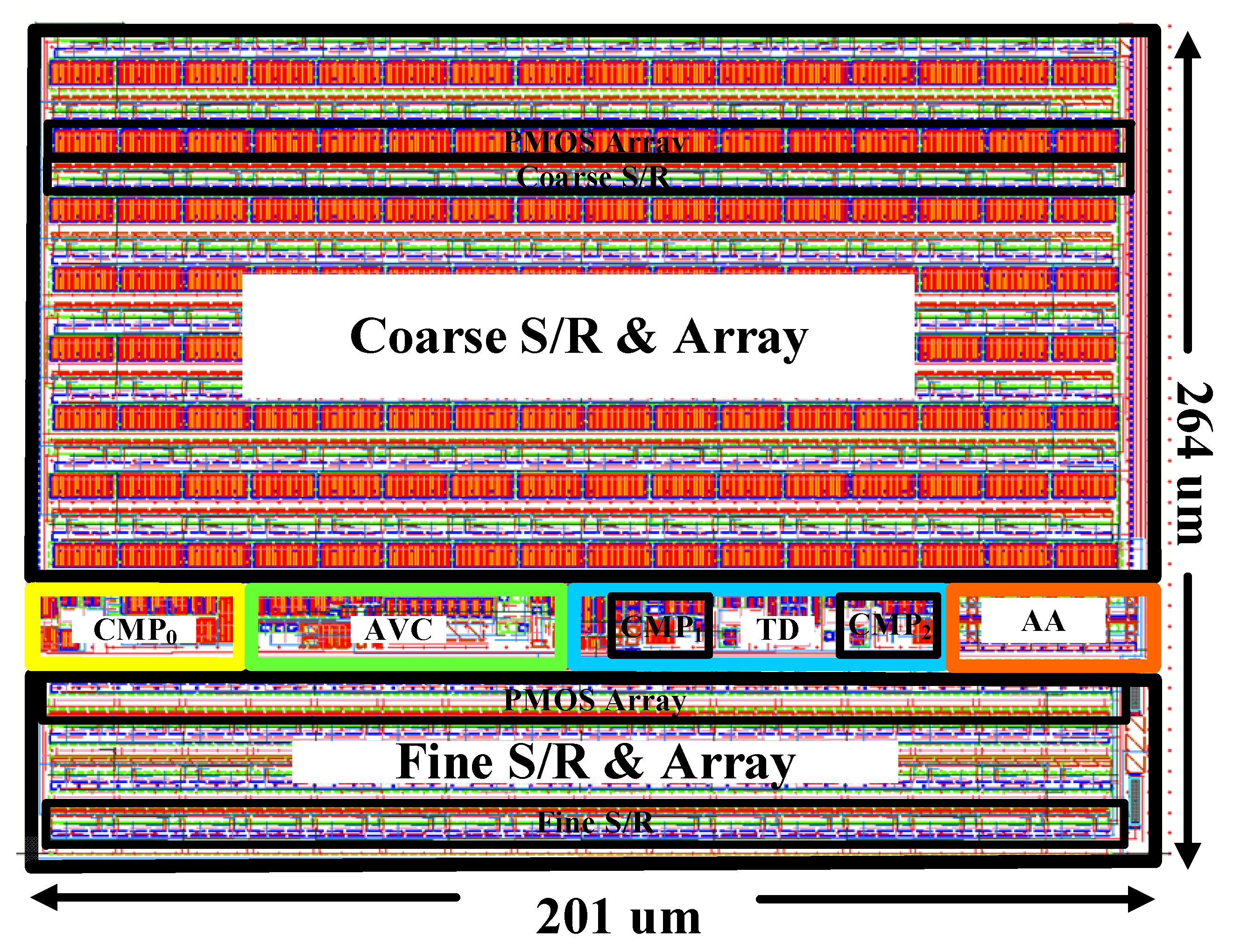
Figure 9 shows that the proposed DLDO occupies an active area of 0.053 mm2 in a standard 0.18 μm CMOS process including the CMP0, the AVC, the TD with two self-clocked comparators (CMP1 and CMP2), the AA circuit, and the coarse and fine S/R and the power PMOS transistor array. 
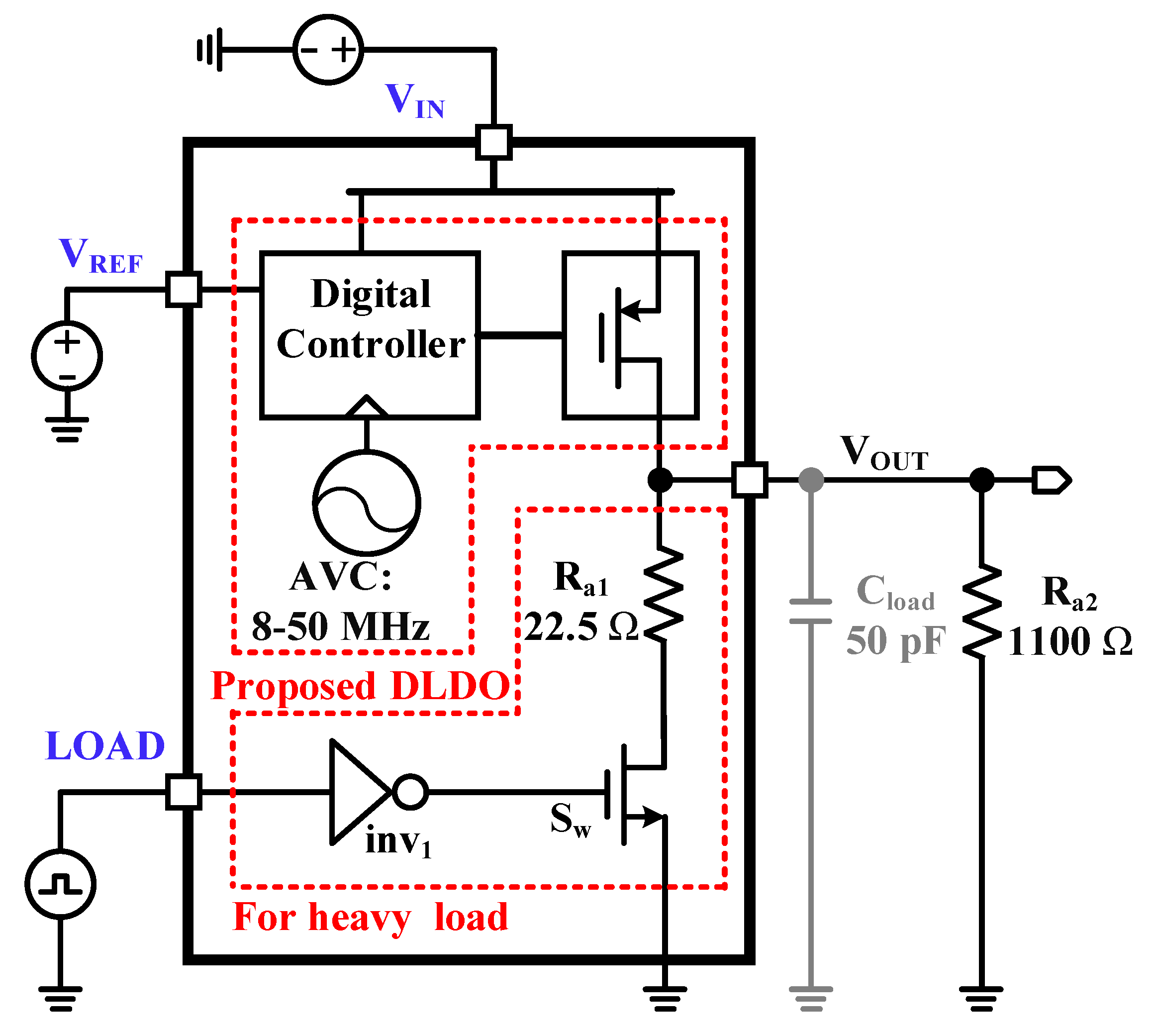
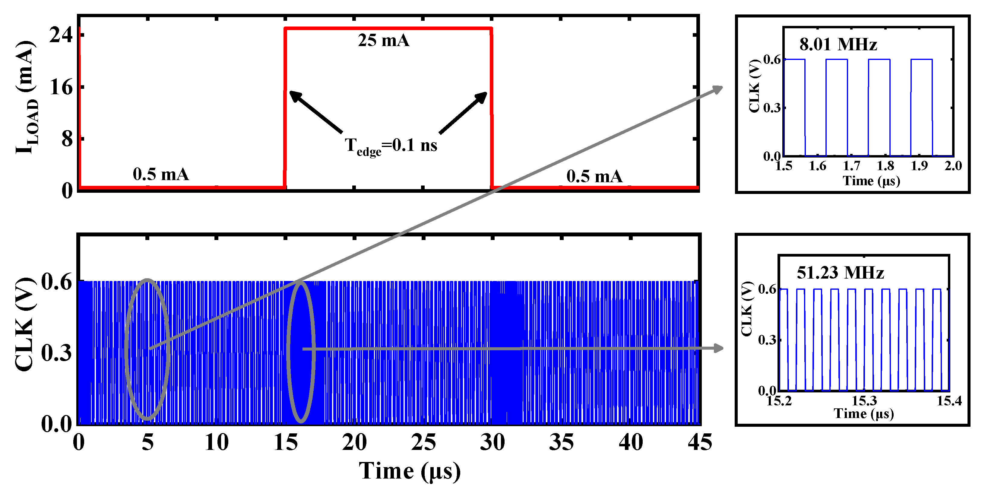
Figure 10 shows the simulation setup of the proposed DLDO. The total on-chip capacitor (CC) was 50 pF and the resistors Ra1 and Ra2 were served for the heavy load and light load, which were designed as 22.5 Ω and 1100 Ω, respectively. The switch (Sw) and the inverter (inv1) are employed to generate the falling and rising edge time of 100 ps for the load transient.
All parasitic effects were considered including the parasitic capacitance from the metal wires to the substrate, the parasitic capacitance among different metal wires, and the parasitic resistance of the wires. The parasitic resistance of the entire proposed DLDO was reduced by the minimum spacing between modules and the multilayer metal interconnection technology. Because the static current of the proposed DLDO was less than 100 μA, the effect of the parasitic resistance was almost negligible. In addition, the offset of the dynamic comparator and resistance mismatch in the TD circuit were suppressed by good matching and dummy technology.
The proposed DLDO provides a load current from 500 μA to 25 mA and consumes a quiescent current of 95.13 μA at the heavy load of 25 mA under a low supply of 0.6 V, resulting in a peak current efficiency of 99.6%. The power consumption is independent of the Iload, and Figure 11 illustrates the power breakdown of the proposed DLDO in the steady state where the resistors in the TD occupy more than 50% of the total power, and the power of the AVC is only 2.5% of the total power.
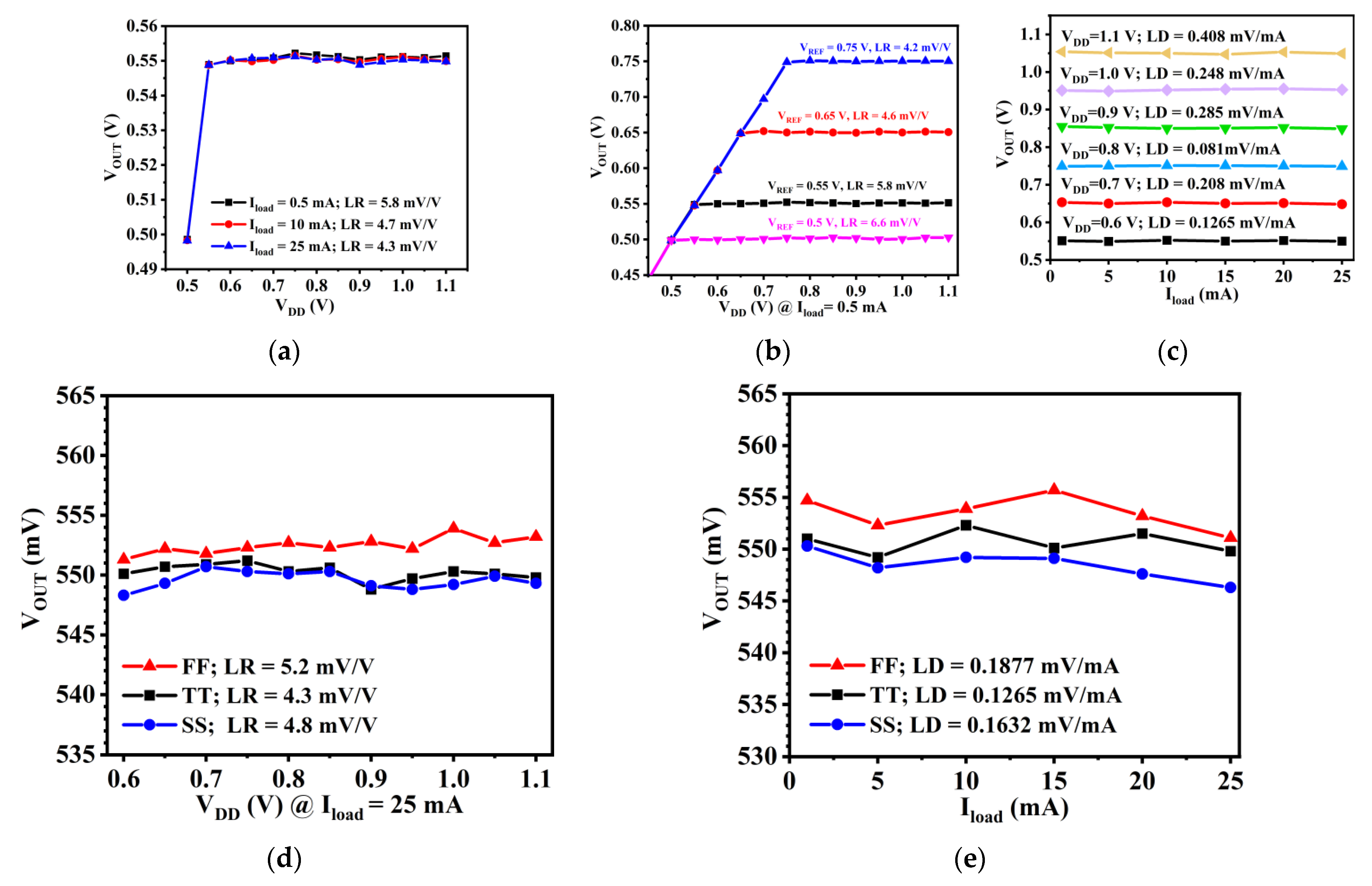
The proposed DLDO can regulate VOUT from 550 mV to 1050 mV with the VDD varying from 0.6 V to 1.1 V with a dropout voltage of 50 mV. Figure 12a shows that the line regulation (LR) was 5.8 mV/V at the load current of 0.5 mA and 4.3 mV/V at the heavy load of 25 mA, respectively, while Figure 12b shows that the best and worst LR were 4.2 mV/V and 6.6 mV/V at the VREF of 0.75 V and 0.5 V, respectively. Figure 12c shows that the fluctuation of the load regulation (LD) varied the supply voltage, and the LD as 0.1265 mV/mA at the supply of 0.6 V. Figure 12d,e verified the LR at the light load of 0.5 mA and LD at the 0.6 V supply at different corners, and the LR and LD remained at the same order of magnitude. To evaluate the transient performance of the proposed DLDO, the proposed DLDO regulator was operated at the VDD of 600 mV with the VOUT of 550 mV and the CC of 50 pF.
Regardless of the analog LDO or the digital LDO, the shorter the Tedge, the more it can reflect the worst undershoot voltage and overshoot voltage of the LDO. Therefore, Tedge was designed to be 100 ps to reflect the worst undershoot voltage and overshoot voltage. The advantage of the capacitor CC in the AA technology is that the off-chip load capacitor can be reduced to 0 [
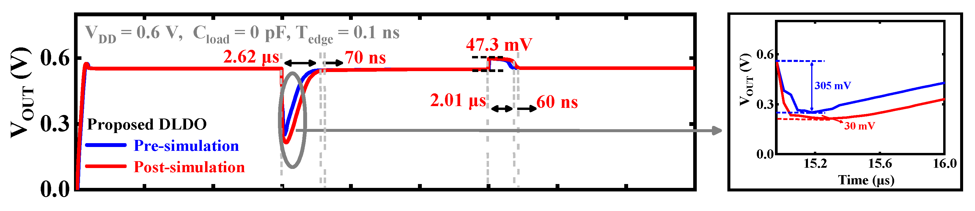
10]. In order to intuitively reflect the transient effects of parasitic capacitance and resistance, Figure 13 shows that the overshoot voltage and undershoot voltage of the proposed DLDO were almost unchanged, and the recovery time of the undershoot and overshoot was extended by 70 ns and 60 ns, respectively.
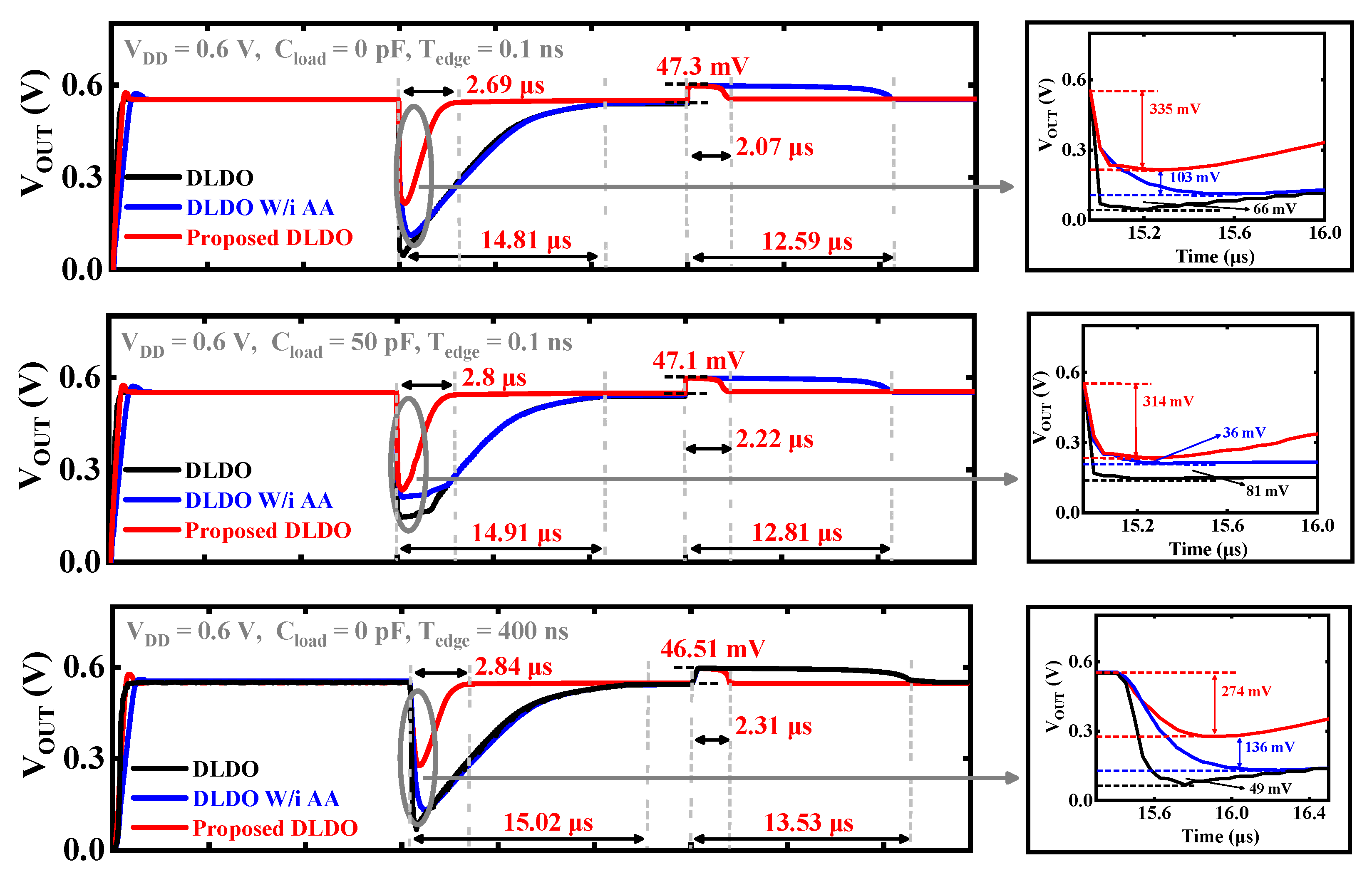
Figure 14 shows the transient response comparison among the conventional LDO, the DLDO with the AA loop, and the proposed double-edge-triggered DLDO with the AA loop and the AVC. At the external clock frequency of 8 MHz, the undershoot voltage of the conventional DLDO with the AA technology decreased by 66 mV than that of the conventional DLDO when the load current stepped up from 0.5 mA to 25 mA at the edge time (Iload) of 100 ps. Compared with the conventional DLDO with the AA technology, the undershoot voltage with the proposed double-edge-triggered DLDO can be reduced from 438 mV to 335 mV, and the recovery time was optimized from 14.8 μs to 2.7 μs in the undershoot case and from 10.5 μs to 2.1 μs in the overshoot case. Meanwhile, it can be seen from Figure 14 that the clock frequency was enhanced from 8 MHz to 50 MHz by the AVC. Figure 14 also shows the transient response of the proposed DLDO with and without a load capacitor at a supply of 0.6 V at the different Tedge. As can be seen from Figure 14, the undershoot voltage with the load capacitor was only 21 mV smaller than that without the load capacitor, while the overshoot voltage was almost constant whether the load capacitor exists or not. This verifies that the CC in the AA technology can reduce the off-chip load capacitor to 0. Furthermore, when the Tedge was 400 ns as in [18], the undershoot voltage and overshoot voltage were decreased to 274 mV and 46.51 mV. 
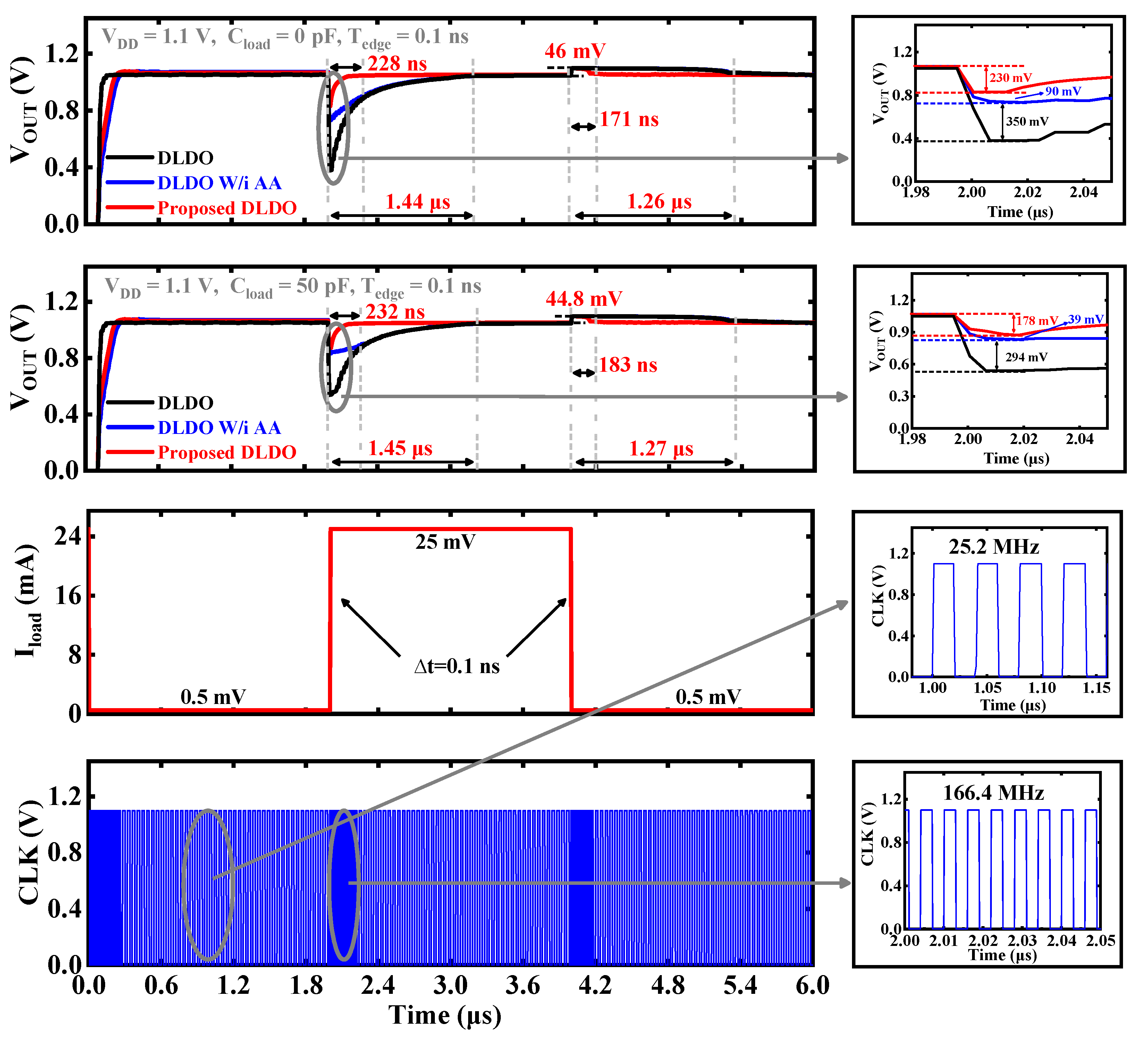
Figure 15 shows the transient response of the proposed DLDO with and without a load capacitor at a supply of 1.1 V. The undershoot voltage and overshoot voltage were 230 mV and 46 mV without the load capacitor, respectively. When a load capacitor (Cload) of 50 pF was added, the undershoot voltage and overshoot voltage decreased to 232 mV and 44.8 mV, respectively. Furthermore, the transient response was also enhanced due to the improvement in the clock frequency of the AVC. Overall, the undershoot voltage and overshoot voltage were optimized with a longer Tedge and a load capacitor.
To verify the robustness of the transient responses, the simulation at different process corners and temperatures is depicted in Table 2. The undershoot voltage and overshoot voltage at the FF corner had a smaller spike, and the recovery time became faster than the performances at the TT corner with the same temperature, while the performances at the SS corner behaved just right, in contrast. As a result, the worst undershoot voltage and overshoot voltage were 399 mV with a recovery time of 2.7 μs and 48.3 mV with a recovery time of 2.1 μs, respectively. The reason why the overshoot voltage was almost constant is that Vout jumped to almost the supply voltage when the output voltage suddenly dropped from 25 mA to 0.5 mA.
Table 3 illustrates the performance parameters of the proposed DLDO in this paper and compares the simulation performances with the state-of-the-art DLDO architectures. In the steady state, the Vdrop voltage is always 50 mV for any supply voltage. Specifically, when the supply voltage is 1.1 V, the output voltage is 1.05 V, while the supply voltage is 600 mV and the output voltage is 550 mV. Compared with [18,19], these DLDOs still need a large load capacitor to suppress the voltage fluctuation within 100 mV during the transient response. Compared to works with a fixed clock frequency [9,19,20,21], the AVC between the steady state and the transient response could better balance the transient responses and static current. Although the load current change could achieve a change of 28 mA in [22] at the only load capacitor of 9.5 pF, the DLDO consumed up to the quiescent current of about 1 mA, which degraded the current efficiency. The proposed DLDO can fix the stability issues at any load current and thus allows the output change from the minimum to the maximum load current within an edge time of 100 ps because the clock frequency can be adaptively adjusted based on the output voltage in time. Moreover, even though the power of the AVC is included, the quiescent current of the entire DLDO is still very low, resulting in the two FoMs. Meanwhile, we provide a comparison of the related simulation results with the previous publications [1,2,23,24] in Table 4 regarding the analog LDOs in electronics. It can be seen from Table 4 that the static power consumption of the recent analog LDOs is comparable to that of the proposed DLDO. Furthermore, the area of these analog LDOs did not include the area of the load capacitor (Cload). The analog LDO could achieve better FoMs than the proposed DLDO because of the small undershoot voltage and overshoot voltage due to a larger load capacitor and a looser Tedge. The main advantages of the proposed DLDO are the ability to achieve an adjustable output voltage, completely circumvent the load capacitor, and a rigorous Tedge of only 0.1 ns at a low power supply (VDD < 1.2 V).

5. Conclusions

A double-edge-triggered DLDO was proposed with a built-in adaptive VCO clock. With the double-edge-trigger technology, the transient response can be enhanced by 2× without any power increment in the DLDO. In addition, the stability is also relaxed due to the low clock frequency, and the mode of the LCO is optimized as 1. Moreover, the built-in adaptive clock can accelerate the clock frequency from 8 MHz to 50 MHz, which balances the recovery time in the transient response and the power consumption in the steady state. The post-simulation results using a standard 0.18 μm CMOS process demonstrated that the maximum current is 99.6% with the self-clock comparators. Furthermore, benefiting from the process scaling, the proposed DLDO will be very suitable for ultra-low-voltage and ultra-low-power integrated digital circuits and systems.

Author Contributions

Conceptualization, X.X., D.W. and X.T.; Methodology, X.X. and D.W.; Validation, X.X. and D.W.; Formal analysis, D.W.; Investigation, X.X.; Resources, X.X. and X.T.; Writing—original draft preparation, X.X.; Writing—review and editing, D.W. and X.T.; Supervision, X.T.; Project administration, X.T.; Funding acquisition, X.X. and X.T. All authors have read and agreed to the published version of the manuscript.

Funding

This work was supported in part by the National Natural Science Foundation of China (No. 62104193, and No. 62271389) and the Key Scientific Research Program of Shaanxi Provincial Department of Education (No. 22JY058).

Data Availability Statement

Data sharing is not applicable to this article as no datasets were generated or analyzed during the current study.

Conflicts of Interest

The authors declare no conflict of interest.

References

  1. Li, Y. A Low-Power, Fast-Transient FVF-Based Output-Capacitorless LDO with Push–Pull Buffer and Adaptive Resistance Unit. Electronics 2023, 12, 1285. [Google Scholar] [CrossRef]
  2. Gao, M. Fully Integrated 1.8 V Output 300 mA Load LDO with Fast Transient Response. Electronics 2023, 12, 1409. [Google Scholar] [CrossRef]
  3. Wang, Z.; Kim, S.J.; Bowman, K.; Seok, M. Review, Survey, and Benchmark of Recent Digital LDO Voltage Regulators. In Proceedings of the 2022 IEEE Custom Integrated Circuits Conference (CICC), Newport Beach, CA, USA, 24–27 April 2022; Volume 52, pp. 1–8. [Google Scholar]
  4. Ma, X.; Lu, Y.; Li, Q.; Ki, W.H.; Martins, R.P. An NMOS Digital LDO With NAND-Based Analog-Assisted Loop in 28-nm CMOS. IEEE Trans. Circuits Syst. I Regul. Pap. 2020, 67, 4041–4052. [Google Scholar] [CrossRef]
  5. Okuma, Y. 0.5-V input digital LDO with 98.7% current efficiency and 2.7-μA quiescent current in 65nm CMOS. In Proceedings of the 2010 IEEE Custom Integrated Circuits Conference (CICC), San Jose, CA, USA, 19–22 September 2010; Volume 54, pp. 1–4. [Google Scholar]
  6. Yang, F.; Mok, P.K. A Nanosecond-Transient Fine-Grained Digital LDO With Multi-Step Switching Scheme and Asynchronous Adaptive Pipeline Control. IEEE J. Solid-State Circuits 2017, 52, 2463–2474. [Google Scholar] [CrossRef]
  7. Akram, M.A.; Hong, W.; Hwang, I.C. Capacitorless Self-Clocked All-Digital Low-Dropout Regulator. IEEE J. Solid-State Circuits 2019, 54, 266–276. [Google Scholar] [CrossRef]
  8. Shi, J.; Zhao, B.; Tang, Z.; Ma, P.; Di, Z. A self-clocked binary-seaching digital low-dropout regulator with fast transient response. IEICE Electron. Express 2020, 17, 20200297. [Google Scholar] [CrossRef]
  9. Qian, L.; Li, D.; Qian, K.; Ye, Y.; Xia, Y.; Mak, T. A Fast-Transient Response Digital Low-Dropout Regulator with Dual-Modes Tuning Technique. IEEE Trans. Circuits Syst. II 2020, 67, 2943–2947. [Google Scholar] [CrossRef]
  10. Huang, M.; Lu, Y.; Seng-Pan, U.; Martins, R.P. An analog-assisted tri-loop digital low-dropout regulator. IEEE J. Solid-State Circuits 2018, 53, 20–34. [Google Scholar] [CrossRef]
  11. Oh, J.; Park, J.E.; Jeong, D.K. A Highly Synthesizable 0.5-to-1.0-V Digital Low-Dropout Regulator with Adaptive Clocking and Incremental Regulation Scheme. IEEE Trans. Circuits Syst. II 2020, 67, 2174–2178. [Google Scholar] [CrossRef]
  12. Babayan-Mashhadi, S.; Lotfi, R. Analysis and Design of a Low-Voltage Low-Power Double-Tail Comparator. IEEE Trans. Very Large Scale Integr. (VLSI) Syst. 2014, 22, 343–352. [Google Scholar] [CrossRef]
  13. Albano, D.; Crupi, F.; Cucchi, F.; Iannaccone, G. A Sub-kT/q Voltage Reference Operating at 150 mV. IEEE Trans. Very Large-Scale Integr. (VLSI) Syst. 2015, 23, 1547–1551. [Google Scholar] [CrossRef]
  14. Huang, M.; Lu, Y.; Sin, S.W.; Seng-Pan, U.; Martins, R.P. A Fully Integrated Digital LDO with Coarse–Fine-Tuning and Burst-Mode Operation. IEEE Trans. Circuits Syst. II 2016, 63, 683–687. [Google Scholar] [CrossRef]
  15. Xu, H.; Abidi, A.A. Analysis and Design of Regenerative Comparators for Low Offset and Noise. IEEE Trans. Circuits Syst. I 2019, 66, 2817–2830. [Google Scholar] [CrossRef]
  16. Huang, M.; Lu, Y.; Sin, S.W.; Seng-Pan, U.; Martins, R.P.; Ki, W.H. Limit Cycle Oscillation Reduction for Digital Low Dropout Regulators. IEEE Trans. Circuits Syst. II 2016, 63, 903–907. [Google Scholar] [CrossRef]
  17. Cai, G.; Zhan, C.; Lu, Y. A Fast-Transient-Response Fully-Integrated Digital LDO With Adaptive Current Step Size Control. IEEE Trans. Circuits Syst. I 2019, 66, 3610–3619. [Google Scholar] [CrossRef]
  18. Lin, J.H.; Yang, S.H.; Muniandi, B.; Ma, Y.S.; Huang, C.M.; Chen, K.H. A High Efficiency and Fast Transient Digital Low-Dropout Regulator with the Burst Mode Corresponding to the Power-Saving Modes of DC–DC Switching Converters. IEEE Trans. Power Electron. 2020, 35, 3997–4008. [Google Scholar] [CrossRef]
  19. Salem, L.G.; Warchall, J.; Mercier, P.P. A Successive Approximation Recursive Digital Low-Dropout Voltage Regulator with PD Compensation and Sub-LSB Duty Control. IEEE J. Solid-State Circuits 2018, 53, 35–49. [Google Scholar] [CrossRef]
  20. Sood, L.; Agarwal, A. A CMOS standard-cell based fully-synthesizable low-dropout regulator for ultra-low power applications. AEU-Int. J. Electron. Commun. 2021, 141, 153958. [Google Scholar] [CrossRef]
  21. Kang, J.G.; Park, J.; Jeong, M.G.; Yoo, C. Digital Low-Dropout Regulator with Voltage-Controlled Oscillator Based Control. IEEE Trans. Power Electron. 2022, 37, 6951–6961. [Google Scholar] [CrossRef]
  22. Cherivirala, Y.K.; Wentzloff, D.D. A Capacitor-Less Digital LDO Regulator with Synthesizable PID Controller Achieving 99.75% Efficiency and 93.3-ps Response Time in 65 nm. IEEE Trans. Circuits Syst. II 2023, 70, 1769–1773. [Google Scholar] [CrossRef]
  23. Perez-Bailon, J.; Calvo, B.; Medrano, N. A Fully-Integrated 180 Nm CMOS 1.2 V Low-Dropout Regulator for Low-Power Portable Applications. Electronics 2021, 10, 2108. [Google Scholar] [CrossRef]
  24. Jiang, Y.; Wang, L.; Wang, S.; Cui, M.; Zheng, Z.; Li, Y. A Low-Power, Fast-Transient Output-Capacitorless LDO with Transient Enhancement Unit and Current Booster. Electronics 2022, 11, 701. [Google Scholar] [CrossRef]
Figure 1. (a) Block diagram of the proposed DLDO. (b) Transient response comparison between the classical and proposed DLDO.
Electronics 12 04100 g001
Figure 3. The 500-run Monte Carlo simulation about the offset voltage. (a) Fclk = 8 MHz; (b) Fclk = 50 MHz.
Electronics 12 04100 g003
Figure 4. (a) Schematic of the AVC. (b) Schematic of the oscillator. (c) Working state.
Electronics 12 04100 g004
Figure 5. The clock frequency (Fclk) of the AVC. (a) Different process corners. (b) The 500-run Monte Carlo simulation.
Electronics 12 04100 g005
Figure 6. (a) Small signal equivalent model; (b) pole-zero analysis.
Electronics 12 04100 g006
Figure 7. (a) Root locus plot of the proposed DLDO. (b) Step response curve at the different Fload with a Fclk of 1.
Electronics 12 04100 g007
Figure 8. Conceptual transient waveform of the LCO phenomenon.
Electronics 12 04100 g008
Figure 9. Layout of the proposed DLDO.
Electronics 12 04100 g009
Figure 10. Simulation setup.
Electronics 12 04100 g010
Figure 11. Power breakdown.
Electronics 12 04100 g011
Figure 12. (a) Simulated LR at the different loads. (b) Simulated LR at different VREF values. (c) Simulated LD at different supplies. (d) Simulated LR at different corners. (e) Simulated LD at different corners.
Electronics 12 04100 g012
Figure 13. Simulated transient comparison between the pre-simulation and post-simulation.
Electronics 12 04100 g013
Figure 14. Simulated transient response comparison with Refs [5,10] at a supply voltage of 0.6 V.
Electronics 12 04100 g014aElectronics 12 04100 g014b
Figure 15. Simulated transient response comparison with Refs [5,10] at a supply voltage of 1.1 V.
Electronics 12 04100 g015
Table 1. Fclk at different temperature and process corners.
Temp [°C]−402785
CornerFFTTSSFFTTSSFFTTSS
Steady state
@ Fclk [MHz]
7.865.974.1210.058.015.1013.1310.967.15
Undershoot @ Fclk [MHz]52.3140.2829.9760.1151.2339.5870.2361.3449.22
Overshoot
@ Fclk [MHz]
51.0339.2428.9257.8849.5438.3769.5860.7748.64
Table 2. Transient response at different temperatures and process corners.
Temp [°C]−40 °C @Iload
from 0.5 to 25 mA
27 °C @Iload
from 0.5 to 25 mA
85 °C @Iload
from 0.5 to 25 mA
CornerFFTTSSFFTTSSFFTTSS
Undershoot
@ Tr [mV/μs]
329354399292335378268296342
2.464.228.581.82.74.31.221.33.01
Overshoot
@ Tr [mV/μs]
47.547.948.346.847.648.145.347.147.9
2.123.787.571.312.14.030.921.022.88
Table 3. Performance summary and comparison with other DLDOs.
JSSC’
18 [19] b
TCAS-II’
20 [9] b
TCAS-II’
20 [11] b
TPE’
20 [18] b
AEU’
21 [20] a
TPE’
22 [21] b
TCAS-II’
23 [22] b
This
Work a
Process
[nm]
65652840456565180
Gen method
of clock
External clockExternal clockExternal clockExternal clockExternal clockVCOExternal clockVCO
Trigger
method
Asyn/
SET
Syn/
SET
Syn/
SET
Asyn/
SET
Syn/
SET
Syn/
SET
Asyn/
SET
Syn/
DET
Clock
Adaptive
YesNOYesNONOYesYesYes
Fclk [MHz]1–240104–6410010500NA8–50
VDD [V]0.5–10.6–1.00.5–10.6–1.10.5–10.9–1.20.7–1.30.6–1.1
Vout [V]0.3–0.450.55–0.950.45–0.950.5–10.45–0.950.5–1.10.65–1.250.55–1.05
Vdrop [mV]505050100501005050
Cload [pF]400100010047005020000
Ctotal [pF]4001000100470050200.59.550
IQ [μA]1410.220.119.622131105095.13
Iload, max [mA]5.64.56.520268025
Iload, min [mA]0.00010.110.40.50.1550.5
∆ILoad [mA]1.06-2191.532824.5
Line
regulation
[mV/V]
2.3---23.8-2.634.3
Load
regulation
[mV/mA]
5.64.40.019611.0070.15-0.1265
Tedge [ns]15.1105400150.10.1
∆VOUT [mV]40118924014080275335
Settling
Time [μs]
0.15.90.0831.31.20.090.00182.7
Peak current efficiency [%]99.899.799.899.999.9899.399.799.6
Area [mm2]0.00230.08960.041730.180.00640.0590.09250.053
FoM1 [ps] [4]199.35962.1646.2310.26.84232.883.4982.654
FoM2 [pF] [11]0.70.6830.2050.3870.2281.3970.150.13
a Simulation results, b Measurement results; SET: Single-edge trigger, DET: Double-edge trigger; FoM1 = Ctotal × ∆Vout × IQ/∆Iload2; FoM2 = Ctotal × ∆Vout × IQ/(Vout × ∆Iload).
Table 4. Performance summary and comparison with other analog LDOs.
Electronics’
21 [23] a
Electronics’
22 [24] a
Electronics’
23 [1] a
Electronics’
23 [2] a
This
Work a
Process
[nm]
180180180180180
ArchitectureALDOALDOALDOALDODLDO
VDD [V]1.297–3.31.2–1.81.82–50.6–1.1
Vout [V]1.211.51.80.55–1.05
Vdrop [mV]9720030020050
Cload [pF]501005050
Ctotal [pF]56.1107.51050550
PowerQ [μW]11.1512.3628.98132.857.07
Iload, max [mA]501005030025
Iload, min [mA]110.230.5
∆ILoad [mA]509949.829724.5
Line
regulation
[mV/V]
0.0652.74-0.554.3
Load
regulation
[mV/mA]
0.0060.03414500.001940.1265
Tedge [ns]1000100103000.1
∆VOUT [mV]66647129153335
Settling
Time [μs]
6.70.190.20.42.7
Peak current efficiency [%]99.999.999.999.999.6
Area [mm2]0.1030.015240.0460.0850.053
FoM1 [ps] [4]0.110.0050.8790.0052.654
FoM2 [pF] [11]0.0050.00050.0290.00010.13
a Simulation results.
Disclaimer/Publisher’s Note: The statements, opinions and data contained in all publications are solely those of the individual author(s) and contributor(s) and not of MDPI and/or the editor(s). MDPI and/or the editor(s) disclaim responsibility for any injury to people or property resulting from any ideas, methods, instructions or products referred to in the content.

