Communication

Characterization and Reliability Analysis of Enhancement-Mode PEALD AlN/LPCVD SiNx GaN MISFET with In Situ H2/N2 Plasma Pretreatment

1
School of Integrated Circuits, Peking University, Beijing 100871, China
2
Shenzhen SoC Key Laboratory, PKU-HKUST Shenzhen-Hong Kong Institution, Shenzhen 518057, China
*
Authors to whom correspondence should be addressed.
Electronics 2023, 12(21), 4482; https://doi.org/10.3390/electronics12214482
Submission received: 31 July 2023 / Revised: 27 September 2023 / Accepted: 27 September 2023 / Published: 31 October 2023
(This article belongs to the Section Microelectronics)

Abstract

:
An effective in situ H2/N2 pretreatment technique for enhancement-mode GaN MISFET with a PEALD AlN/LPCVD SiNx Dual Gate Dielectric is presented. This technique features in situ H2 (15%)/N2 (85%) plasma pretreatment prior to AlN deposition. By using in situ H2 (15%)/N2 (85%) plasma pretreatment and a PEALD AlN protection layer, combined with an LPCVD SiNx gate dielectric, the quality of the AlN/GaN interface can be further improved due to the reduced interface trap densities between the AlN/GaN interface. The interface protection technique enables the successful integration of a high-quality PEALD AlN/LPCVD SiNx gate dielectric in an E-mode GaN MISFET with high performance, high stability, and high reliability. The fabricated enhancement-mode GaN MISFET exhibits a high gate swing and high channel effective mobility of 187.5 cm2/Vs, a threshold voltage of 2.9 V defined at 1 µA/mm, an on/off current ratio of 108, and a breakdown voltage of 1760 V defined at ID = 10 μm/mm. Our experiments showed a significant reduction in dynamic ON resistance and the suppression of current collapse when using the enhancement-mode GaN MISFET with PEALD AlN/LPCVD SiNx under high drain bias switching conditions, especially when the VDS is greater than the 60 V drain bias switch operating state.

1. Introduction

As a wide band gap semiconductor material, GaN has a bright future in the field of power semiconductor devices due to its advantages of high thermal conductivity, a high breakdown electric field, and high electron saturation drift velocity. Two-dimensional electron gas (2DEG) with high concentration and high mobility could be formed in the AlGaN/GaN interface due to its strong polarization effect in III-nitrides. Gallium nitride-based high electron mobility transistors (HEMT) could provide low ON resistance, fast switching speed, and high-power handling ability in power switching applications [1]. However, the channel of traditional AlGaN/GaN HEMT is very close to the material interface, so the phenomenon of current collapse is caused by the interface state [1,2,3], especially under the condition of high drain voltage switching [4,5]. Various techniques are used to suppress current collapse, such as PECVD SiN surface passivation technology [6,7,8,9,10,11]; moreover, it is combined with field plate technology to suppress current collapse. In addition, various surface pretreatment techniques are used to improve interface quality and suppress current collapse [12,13]. In situ low-damage plasma pretreatment can remove primary oxides on the surface and minimize surface damage [14,15,16]. In situ PR passivation of plasma surfaces, such as NH3 [17,18] or N2O [13], has been proven to suppress current collapse and improve AlGaN/GaN HEMT reliability [19,20,21]. Research work on the switch features of PEALD AlN/LPCVD SiNx Dual Gate Dielectric power HEMTs switching from the OFF-state at a high drain bias larger than 200 V is very rare [22,23,24,25].
In this paper, the research results demonstrate an effective in situ H2 (15%)/N2 (85%) pretreatment technique for gate-recessed enhancement-mode GaN MISFET with a PEALD AlN/LPCVD SiNx Dual Gate Dielectric. The feature of the technique is an in situ H2 (15%)/N2 (85%) plasma pretreatment prior to AlN deposition. By using in situ H2 (15%)/N2 (85%) plasma pretreatment and a PEALD AlN protection layer, combined with an LPCVD SiNx gate dielectric, the channel interface quality can be further improved due to the reduced interface trap densities between the AlN/GaN interface. Experiments have proven that current collapse suppression and dynamic ON resistance significantly reduce the normally-off GaN MISFET with PEALD AlN/LPCVD SiNx under high drain bias switching conditions.

2. Device Fabrication

The AlGaN/GaN epitaxial structure studied here was grown in 6-inch p-type (111) Si substrates by metal-organic chemical vapor deposition (MOCVD). This includes the GaN buffer layer (4.2 μm), GaN channel layer (420 nm), AlN spacer layer (0.7 nm), Al0.25Ga0.75N barrier layer (24.5 nm), and GaN cap layer (2.4 nm). Device fabrication commenced with gate region definition by optical lithography, and the photoresist was used as a mask; the GaN cap layer of the opened regions was removed by SF6-based reactive ion etching (RIE). The etching rate of the GaN cap layer was about 1 nm/min. Then, the GaN cap layer was used as a recess mask; the AlGaN barrier layer was effectively eliminated through a two-step process [26,27]. In the first step, thermal oxidation was performed at 650 °C for 50 min in the l4,508 tube annealing furnace. Taking advantage of the easy oxidation of Al atoms in AlGaN materials, the N atoms around Al atoms are replaced by O atoms to form Al-O bonds or Al-O-Ga bonds during oxidation at high temperatures. The oxidized AlGaN layer can be corroded using hot alkali solution. However, GaN material will not be oxidized at 650 °C and will be oxidized at higher temperatures. Therefore, as long as the oxidation temperature and time are well controlled, only the AlGaN material can be oxidized, the GaN material will not be oxidized, and oxidation will stop at the AlGaN/GaN interface.
The second step involves wet corrosion by TMAH solution treatment at 80 °C for 60 min. The products (AlOx and GaOx) of the AlGaN layer after high-temperature oxidation can be corroded by an alkali solution. The Ga-plane gallium nitride material cannot be effectively corroded by the alkali solution at 25 °C to 85 °C, so the corrosion can stop at the AlGaN/GaN interface. Figure 1a presents the AFM image and the corresponding depth curve of the recessed gate formed after high-temperature oxidation and TMAH corrosion, clearly demonstrating the complete removal of the barrier layer after thermal oxidation and wet etching. Then, gate dielectric deposition is carried out. The thickness of the PEALD AlN and LPCVD SiNx were 5 nm and 30 nm, respectively, and various in situ plasma treatments were performed in the ANAME Elegant I PEALD system before the PEALD AlN was deposited. Ohmic contact Ti/Al/Ni/Au (22/140/55/44 nm) metal stacks were fabricated by e-beam evaporation followed by rapid thermal annealing for 30 s at 870 °C. The device planar isolation was formed by F-ion implantation. Finally, the gate region was defined by lithography techniques, and the Ni/Au gate metal stack was completed by e-beam evaporation.
Three kinds of samples of enhancement mode, also known as normally-off mode GaN MISFET with PEALD AlN/LPCVD SiNx, were fabricated by different interface processing pretreatments: Sample 1, without pretreatment; Sample 2, with 400 W in situ NH3 plasma pretreatment for 2 min before the PEALD AlN was deposited; and Sample 3, with 400 W in situ H2(15%)/N2(85%) plasma pretreatment for 2 min before the PEALD AlN was deposited. The fabricated devices had sizes of LGS/LG/LGD/W = 2/2/20/20 μm. The schematic structure of the fabricated enhancement-mode PEALD AlN/LPCVD SiNx Dual Gate dielectric GaN MISFET is shown in Figure 1b.

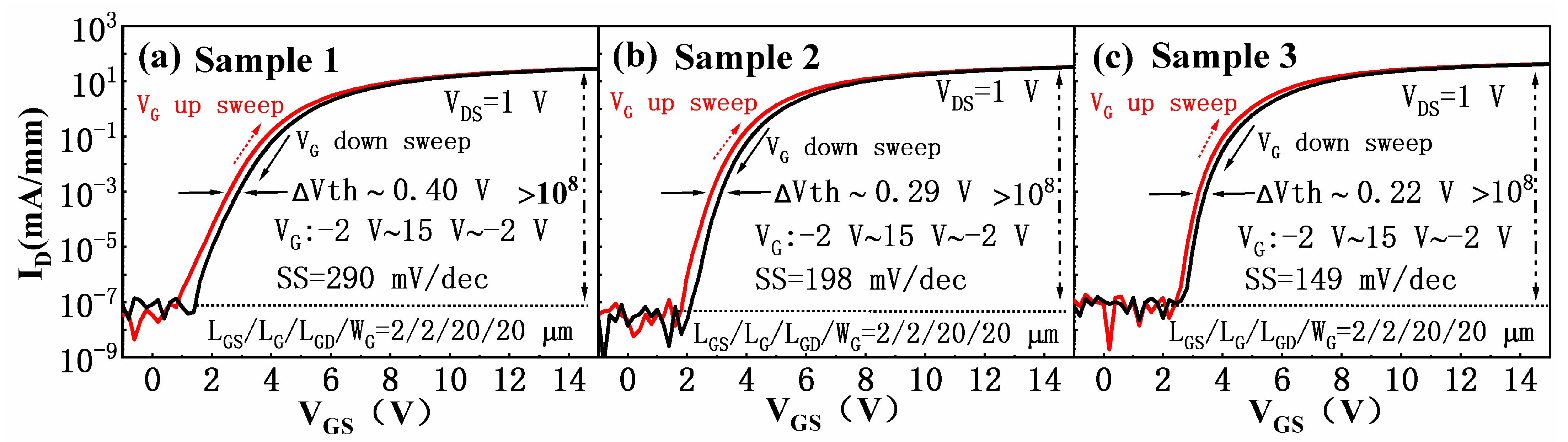
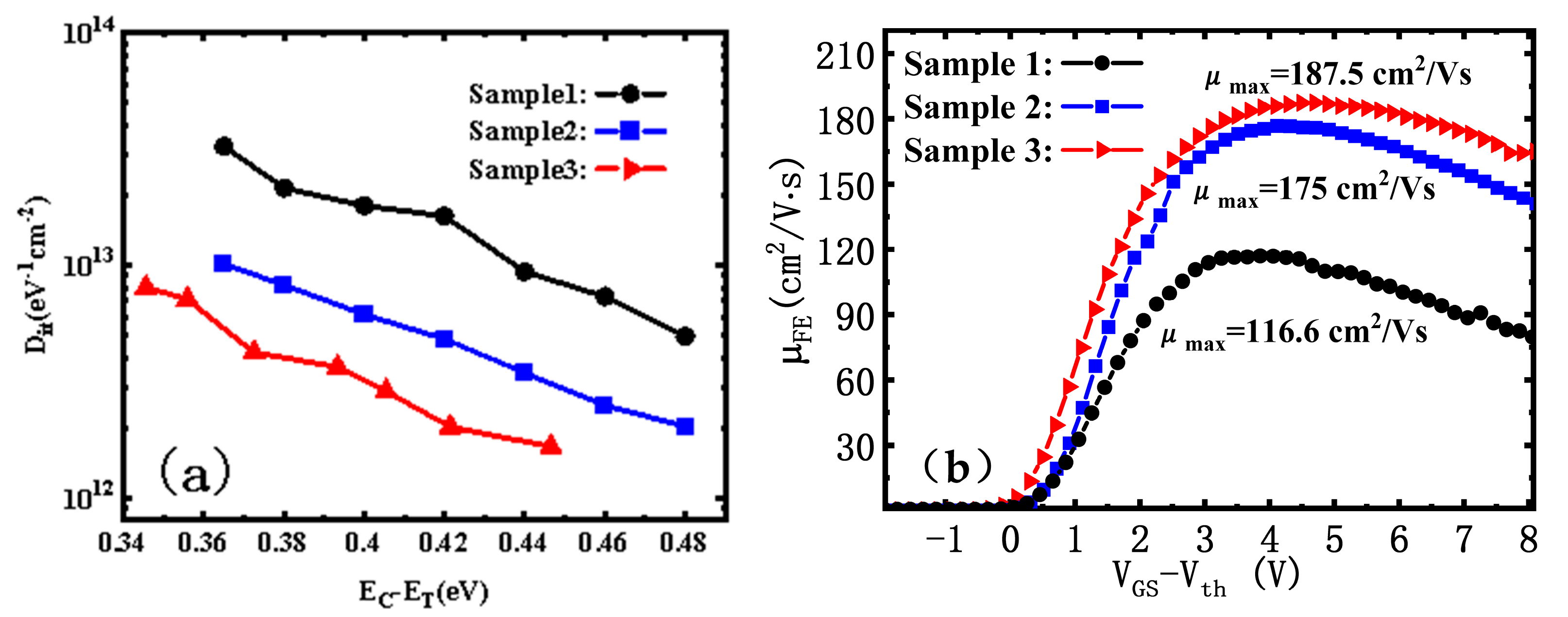
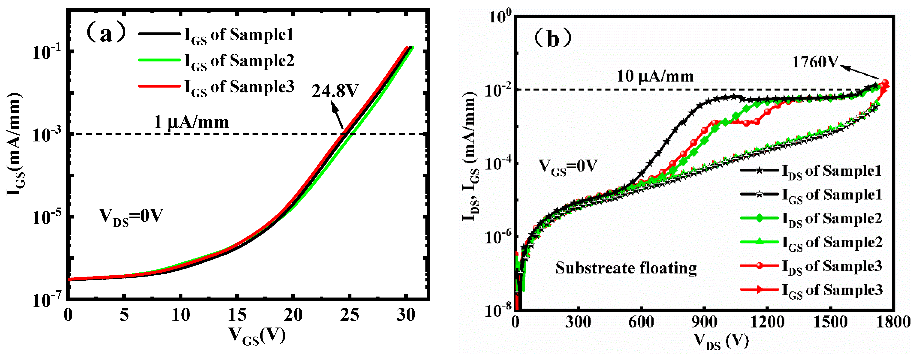
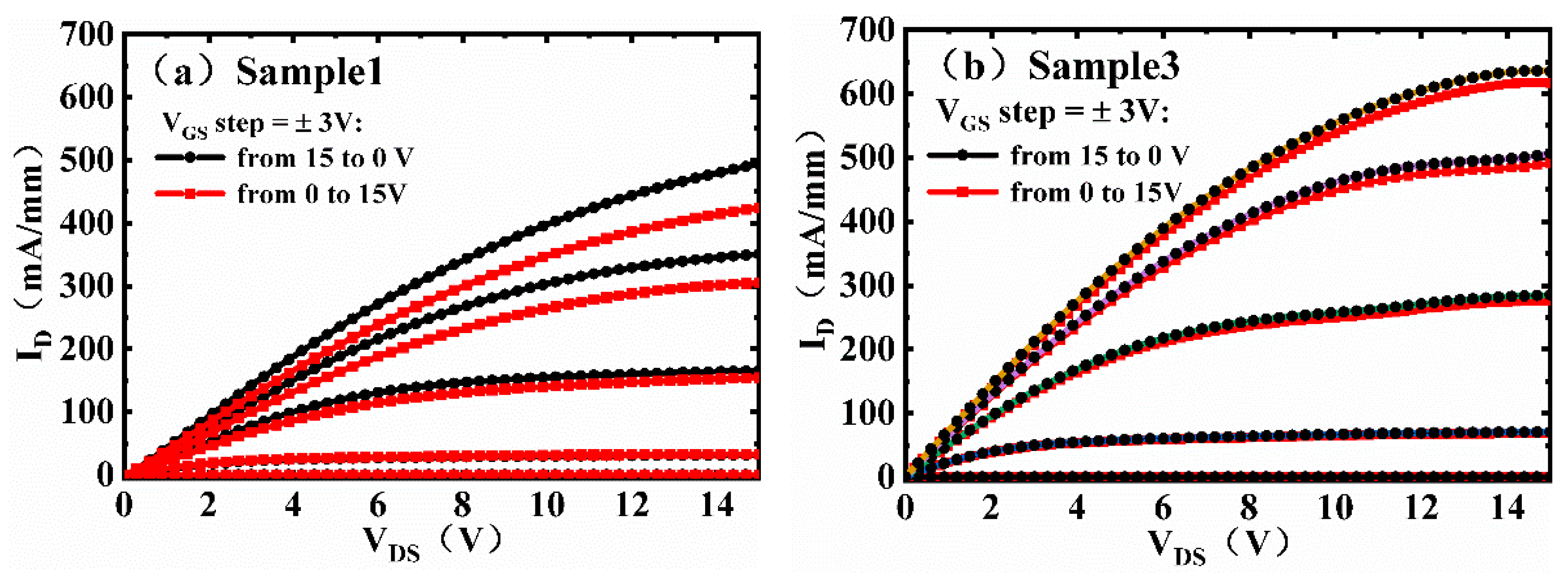
3. Results and Discussion

The electrical properties of the fabricated enhancement-mode PEALD AlN/LPCVD SiNx GaN MISFET were measured by an Agilent B1505A Semiconductor Device Analyzer. Figure 2a demonstrates the transfer characteristics of the fabricated devices with VDS = 15 V in a linear scale. The voltage of VGS swept from −2 to 15 V, and the threshold voltage Vth was determined to be 2.6 V, 2.8 V, and 2.9 V at the drain current criterion of 1 µA/mm for Sample 1, Sample 2, and Sample 3, respectively. The geometrical dimensions of the samples had a gate-source distance (LGS) of 2 μm, a gate length (LG) of 2 μm, a gate-drain distance (LGD) of 20 μm, and a gate width (WG) of 20 μm. The IDmax was ~492 mA/mm, ~601 mA/mm, and ~631 mA/mm for Sample 1, Sample 2, and Sample 3, respectively, and the peak transconductance (Gm) values were ~58 mS/mm, ~76.2 mS/mm, and ~80.25 mS/mm for Sample 1, Sample 2, and Sample 3, respectively. The IDmax of Sample 3 increased by 28% compared with that of Sample 1 and 5% compared with that of Sample 2. Figure 2b shows the output characteristics of the devices. The Ron values of Sample 1, Sample 2, and Sample 3 were 18.3 Ω·mm, 15.9 Ω·mm, and 13.6 Ω·mm, respectively. The Ron of Sample 3 decreased by 33.6% compared with that of Sample 1 and by 14.6% compared with that of Sample 2.
Figure 3 shows the ID-VGS transfer curves of Sample 1, Sample 2, and Sample 3 on a semi-log scale at VDS = 1V. The device is completely turned off at 0 V gate bias, and a truly enhanced operation is achieved. The drain current on/off ratio of the three sample devices is beyond 10 8 . The hysteresis values of the Vth between the VG up and down sweep transfer curves were 0.40 V, 0.29 V, and 0.22 V for Sample 1, Sample 2 and Sample 3, respectively. The sub-threshold swing (SS) was 290 mV/dec, 198 mV/Dec, and 149 mV/dec for Sample 1, Sample 2, and Sample 3, respectively. The threshold voltage hysteresis of Sample 3 is very small because the in situ H2 (15%)/N2 (85%) plasma pretreatment prior to AlN deposition can effectively reduce the interface state density of the AlN/GaN.
In order to analyze the improvement effect of pretreatment channel interface quality and evaluate the interface trap distribution of samples 1, 2, and 3 using the conductance method [10], the conductance method was adopted in the MIS capacitor ring with a radius of 40 μm to extract the AlN/GaN interface trap density of the three samples, as shown in Figure 4a. Among the three samples, Sample 3 had the lowest interface trap concentration, which was about one order of magnitude lower than Sample 1. It can be seen that the AlN/GaN interface trap density (Dit) could be effectively reduced by using the PEALD AlN dielectric combined with in situ H2 (15%)/N2 (85%) plasma pretreatment.
In addition, the field effect mobility at low fields ( μ F E ) for the three samples is also extracted in the linear region (Vds = 0.1 V), as shown in Figure 4b, by calculating the effective mobility based on μ F E = G m L / W C o x V D S   [6], where L is the gate length, W is the gate width, Cox is the dielectric capacitor measured from the FAT-FET device with LG = 100 µm, and Gm is extracted from the transfer characteristic curves at VDS = 0.1 V. The maximum field effect mobility ( μ F E m a x ) values for Sample 1, Sample 2, and Sample 3 were 116.6 cm2/Vs, 175 cm2/Vs, and 187.5 cm2/Vs, respectively. The mobility of Sample 3 was the highest due to the interface trap concentration inhibited by using the PEALD AlN dielectric combined with in situ H2 (15%)/N2 (85%) plasma pretreatment.
Figure 5a illustrates the gate leakage current of the PEALD AlN/LPCVD SiNx GaN MISFET with a grounded source and drain. The gate voltage is defined as the gate breakdown voltage at an IG of 1 μA/mm. It can be observed from Figure 5a that plasma pretreatment did not have an impact on the gate leakage current. Due to the high quality of the double-layer dielectric material, the gate leakage remains below 1 µA/mm until VGS reaches 24.8 V. The high critical breakdown field strength of the double-layer dielectric indicates that the fabricated enhancement-mode GaN MISFET exhibits a high gate swing. Figure 5b presents the breakdown voltage characteristics of samples 1, 2, and 3 with a floating substrate and VGS = 0 V. Sample 3 demonstrates a strong ability to block the current when VGS= 0 V with a breakdown voltage of 1760 V. These data show that within the range of 0–560 V for drain voltage VDS, the gate current IGS is equivalent to the drain current IDS, and increases with an elevated VDS, which indicates the predominant role of gate-drain leakage current at this stage. In the range of 560–1100 V for drain voltage VDS, the increase rate of IDS surpasses that of IGS significantly, indicating that the buffer layer leakage Ivertical begins to play a leading role in IDS. When the VDS is in the range of 1100–1760 V, the IDS remain relatively stable. However, there is a rapid surge in IDS with the increase in VDS, resulting in device breakdown when VDS exceeds 1760 V.
The output characteristics of samples 1 and 3 with VGS step up (or down) from (or toward) below the threshold voltage Vth, as shown in Figure 6a,b. The drain current of Sample 1 in the high gate bias region was significantly lower when the gate bias stepped up from below the threshold voltage. This indicates that there is significant current collapse without pretreatment in Sample 1. For Sample 3, the drain current difference was very small between the gate bias voltage step-up and step-down, indicating that the in situ H2(15%)/N2(85%) plasma pretreatment inhibited current collapse.
To demonstrate the Vth thermal stability, we conducted the transfer characterizations at a temperature ranging from 25 °C to 100 °C in DC mode. The temperature-dependent transfer characteristics in the DC mode of the PEALD AlN/LPCVD SiNx MISFET with in situ H2/N2 plasma pretreatment were measured with a VGS sweeping rate of 0.7 V/s, a step of 0.1 V, and VDS = 8 V. Figure 7 shows the transfer characteristics of the PEALD AlN/LPCVD SiNx MISFET with and without in situ H2/N2 plasma pretreatment.
The temperature dependence of Vth (defined at ID = 1μA/mm) in PEALD AlN/ LPCVD SiNx MISFETs with and without in situ H2/N2 plasma pretreatment is shown in Figure 8. Owing to the reduced interface trap density, the MISFET with in situ H2/N2 plasma pretreatment shows a much smaller VTH shift up to −0.12 V from room temperature to 100 °C than that of the MISFET without in situ H2/N2 plasma pretreatment. It has been proven that the device has good VTH thermal stability. However, it should be noted that the study described in [27] did not include an investigation of this aspect.
In order to further study the effect of pretreatment process suppression on current collapse, the current collapse in the normally-off GaN MISFET with PEALD AlN/LPCVD SiNx under high drain bias switching conditions was characterized. In the OFF-state stress stage, a gate bias VG = 0 V lower than the threshold voltage is applied to the gate of the device to make the device reliably in the OFF-state, while VDS is swept from 0 V to the present value (such as 30, 60, and 90 V). The OFF-state stress duration is 46 s; at the end of the OFF-state stress, the voltage VG = 12 V, and VDS = 1 V is rapidly applied to switch the device from the OFF-state to the ON-state, and the switching time is equal to 70 ms. By monitoring the test characteristics, an ID current of not less than 120 mA/mm was obtained. The output characteristics were measured at the moment the device transitioned from the OFF-state to the ON-state to evaluate dynamic resistance. White light was illuminated on the sample after each OFF-state to ON-state sweep to effectively refresh the devices. The output characteristics of samples 1, 2, and 3 were tested using the above method, and the results are shown in Figure 9. The output characteristics in the absence of any drain bias stress are defined as “Fresh” states. As can be seen from Figure 9a,b, the phenomenon of current collapse is obvious in samples 1 and 2, which becomes more serious with the increase in OFF-state drain bias. Sample 3 exhibits much smaller current collapse, as shown in Figure 9c. The role of in situ H2/N2 pretreatment is mainly reflected in two aspects. First, because the plasma has higher energy, it can remove suboxide in the channel. Second, the N element in plasma can fill the N vacancy in semiconductor material, and the H element can react with surface oxide to remove the surface oxide layer. Thus, the oxygen concentration at the AlN/GaN interface is reduced and the slow response interfacial states caused by oxygen are reduced, which improves the interface quality [9,24]. These results indicate a significant reduction in dynamic ON resistance and the suppression of current collapse under high drain bias switching conditions of 180 V. From a reliability viewpoint, these findings differ from the reference [27].
For various LGD devices, normalized dynamic Ron values of samples 1, 2, and 3 with varied OFF-state drain bias stress are shown in Figure 10. When the drain bias stress is greater than 60 V, the dynamic resistance of Sample 1 increases rapidly, while that of Sample 2 and Sample 3 increases very slowly, and the dynamic resistance of Sample 3 remains at a very small value. Therefore, in situ H2/N2 plasma pretreatment inhibits current collapse and achieves very low dynamic resistance.

4. Conclusions

An effective in situ H2/N2 pretreatment technique for enhancement-mode fully-recessed GaN MISFET with a PEALD AlN/LPCVD SiNx Dual Gate Dielectric has been demonstrated in this study. Through research on the traps at the AlN/GaN interface and dynamic Ron for the normally-off PEALD AlN/LPCVD SiNx GaN MISFETs with and without in situ H2 (15%)/N2 (85%) plasma pretreatment, it was found that this pretreatment leads to a significant reduction in dynamic ON resistance and the suppression of current collapse under high drain bias switching conditions, thereby reducing device transmission loss and improving reliability and channel interface quality. This work can be used as a reference for further optimization of enhancement-mode GaN MISFET devices of Si substrate.

Author Contributions

Conceptualization, C.H. and M.L.; methodology, J.W.; software, B.Z.; validation, C.H., M.L., and J.H.; formal analysis, M.L.; investigation, M.W.; data curation, C.H.; writing—review and editing, C.H. and J.H.; supervision, J.W. and Y.H.; project administration, Y.H. All authors have read and agreed to the published version of the manuscript.

Funding

This research was funded by the Shenzhen Science and Technology Program, IER Funding of PKU-HKUST Shenzhen-Hong Kong Institution (IER202105), grant numbers JCYJ20200109144612399 and JCYJ20220818103408018. This work was supported by the research staff of Atomic Nano-Materials and Equipment Company Ltd. (ANAME).

Data Availability Statement

Not applicable.

Acknowledgments

The aluminum nitride layers used in this manuscript were prepared by ELEGANT II Y300 ALD equipment from Atomic Nano-Materials and Equipment Company Ltd. (ANAME, Nanjing, Jiangsu, China). The authors would like to thank the research staff of ANAME for their expertise in ALD technology and their contribution to optimizing the said material.

Conflicts of Interest

The authors declare no conflict of interest.

References

  1. Chen, K.; Haberlen, O.; Lidow, A.; Tsai, C.; Ueda, T.; Uemoto, Y.; Wu, Y. GaN-on-Si Power Technology: Devices and Applications. IEEE Trans. Electron. Devices 2017, 64, 779–795. [Google Scholar] [CrossRef]
  2. Liu, W.; Sayed, I.; Gupta, C.; Li, H.; Keller, S.; Mishra, U. An improved methodology for extracting interface state density at Si3N4/GaN. Appl. Phys. Lett. 2020, 116, 22104–22107. [Google Scholar] [CrossRef]
  3. Jiang, H.; Liu, C.; Chen, Y.; Lu, X.; Tang, C.; Lau, K. Investigation of In Situ SiN as Gate Dielectric and Surface Passivation for GaN MISHEMTs. IEEE Trans. Electron. Devices 2017, 64, 832–839. [Google Scholar] [CrossRef]
  4. Jauss, S.; Hallaceli, K.; Mansfeld, S.; Schwaiger, S.; Daves, W.; Ambacher, O. Reliability Analysis of LPCVD SiN Gate Dielectric for AlGaN/GaN MIS-HEMTs. IEEE Trans. Electron. Devices 2017, 64, 2298–2305. [Google Scholar] [CrossRef]
  5. Choi, Y.; Pophristic, M.; Cha, H.; Peres, B.; Spencer, M.; Eastman, L. The Effect of an Fe-doped GaN Buffer on off-State Breakdown Characteristics in AlGaN/GaN HEMTs on Si Substrate. IEEE Trans. Electron. Devices 2006, 53, 2926–2931. [Google Scholar] [CrossRef]
  6. Hsieh, T.; Chang, E.; Song, Y.; Lin, Y.; Wang, H.; Liu, S.; Salahuddin, S.; Hu, C. Gate Recessed Quasi-Normally OFF Al2O3/AlGaN/GaN MIS-HEMT with Low Threshold Voltage Hysteresis Using PEALD AlN Interfacial Passivation Layer. IEEE Electron. Device Lett. 2014, 35, 732–734. [Google Scholar]
  7. Zhu, J.; Zhu, Q.; Chen, L.; Hou, B.; Yang, L.; Zhou, X.; Ma, X.; Hao, Y. Impact of Recess Etching on the Temperature-Dependent Characteristics of GaN-Based MIS-HEMTs with Al2O3/AlN Gate-Stack. IEEE Trans. Electron. Devices 2017, 64, 840–847. [Google Scholar] [CrossRef]
  8. Hua, M.; Lu, Y.; Liu, S.; Liu, C.; Fu, K.; Cai, Y.; Zhang, B.; Chen, K. Compatibility of AlN/SiNxPassivation with LPCVD-SiNxGate Dielectric in GaN-Based MIS-HEMT. IEEE Electron. Device Lett. 2016, 37, 265–268. [Google Scholar] [CrossRef]
  9. Kim, K.; Jung, S.; Kim, D.; Kang, H.; Im, K.; Oh, J.; Ha, J.; Shin, J.; Lee, J. Effects of TMAH Treatment on Device Performance of Normally Off Al2O3 GaN MOSFET. IEEE Electron. Device Lett. 2011, 32, 1376–1378. [Google Scholar] [CrossRef]
  10. Jiang, Y.; Wang, Q.; Zhang, F.; Li, L.; Zhou, D.; Liu, Y.; Wang, D.; Ao, J. Reduction of leakage current by O2 plasma treatment for device isolation of AlGaN/GaN heterojunction field-effect transistors. Appl. Surf. Sci. 2015, 351, 1155–1160. [Google Scholar] [CrossRef]
  11. Liu, C.; Yang, S.; Liu, S.; Tang, Z.; Wang, H.; Jiang, Q.; Chen, K. Thermally Stable Enhancement-Mode GaN Metal-Isolator-Semiconductor High-Electron-Mobility Transistor with Partially Recessed Fluorine-Implanted Barrier. IEEE Electron. Device Lett. 2015, 36, 318–320. [Google Scholar] [CrossRef]
  12. Choi, W.; Ryu, H.; Jeon, N.; Lee, M.; Cha, H.; Seo, K. Improvement of Vth Instability in Normally-Off GaN MIS-HEMTs Employing PEALD-SiNx as an Interfacial Layer. IEEE Electron. Device Lett. 2014, 35, 30–32. [Google Scholar] [CrossRef]
  13. Lee, J.; Park, C.; Kim, K.; Kim, D.; Lee, J. Performance of Fully Recessed AlGaN/GaN MOSFET Prepared on GaN Buffer Layer Grown with AlSiC Precoverage on Silicon Substrate. IEEE Electron. Device Lett. 2013, 34, 975–977. [Google Scholar] [CrossRef]
  14. Zhou, Q.; Liu, L.; Zhang, A.; Chen, B.; Jin, Y.; Shi, Y.; Wang, Z.; Chen, W.; Zhang, B. 7.6 V Threshold Voltage High-Performance Normally-Off Al2O3/GaN MOSFET Achieved by Interface Charge Engineering. IEEE Electron. Device Lett. 2016, 37, 165–168. [Google Scholar] [CrossRef]
  15. Feng, Q.; Tian, Y.; Bi, Z.; Yue, Y.; Ni, J.; Zhang, J.; Hao, Y.; Yang, L. The improvement of Al2O3/AlGaN/GaN MISHEMT performance by N2 plasma pretreatment. Chin. Phys. B 2009, 18, 3014–3017. [Google Scholar]
  16. Zhang, Z.; Li, W.; Fu, K.; Yu, G.; Zhang, X.; Zhao, Y.; Sun, S.; Song, L.; Deng, X.; Xing, Z.; et al. AlGaN/GaN MIS-HEMTs of Very-Low Vth Hysteresis and Current Collapse with In-Situ Pre-Deposition Plasma Nitridation and LPCVD-Si3N4 Gate Insulator. IEEE Electron. Device Lett. 2017, 38, 236–239. [Google Scholar] [CrossRef]
  17. Zhang, Z.; Hua, M.; He, J.; Tang, G.; Qian, Q.; Chen, K. Ab initio study of impact of nitridation at amorphous-SiNx/GaN interface. Appl. Phys. Express 2018, 11, 81003–81006. [Google Scholar] [CrossRef]
  18. Sun, N.; Huang, H.; Sun, Z.; Wang, R.; Li, S.; Tao, P.; Ren, Y.; Song, S.; Wang, H.; Li, S.; et al. Improving Gate Reliability of 6-In E-Mode GaN-Based MIS-HEMTs by Employing Mixed Oxygen and Fluorine Plasma Treatment. IEEE Trans. Electron. Devices 2022, 69, 82–87. [Google Scholar] [CrossRef]
  19. Saito, W.; Takada, Y.; Kuraguchi, M.; Tsuda, K.; Omura, I. Recessed-gate structure approach toward normally off high-Voltage AlGaN/GaN HEMT for power electronics applications. IEEE Trans. Electron. Devices 2006, 53, 356–362. [Google Scholar] [CrossRef]
  20. Setera, B.; Christou, A. Challenges of Overcoming Defects in Wide Bandgap Semiconductor Power Electronics. Electronics 2021, 11, 10. [Google Scholar] [CrossRef]
  21. Wang, Y.; Liang, Y.; Samudra, G.; Huang, H.; Huang, B.; Huang, S.; Chang, T.; Huang, C.; Kuo, W.; Lo, G. 6.5 V High Threshold Voltage AlGaN/GaN Power Metal-Insulator-Semiconductor High Electron. Mobility Transistor Using Multilayer Fluorinated Gate Stack. IEEE Electron. Device Lett. 2015, 36, 381–383. [Google Scholar] [CrossRef]
  22. Oka, T.; Nozawa, T. AlGaN/GaN Recessed MIS-Gate HFET with High-Threshold-Voltage Normally-Off Operation for Power Electronics Applications. IEEE Electron. Device Lett. 2008, 29, 668–670. [Google Scholar] [CrossRef]
  23. Zhou, Q.; Chen, B.; Jin, Y.; Huang, S.; Wei, K.; Liu, X.; Bao, X.; Mou, J.; Zhang, B. High-Performance Enhancement-Mode Al2O3/AlGaN/GaN-on-Si MISFETs with 626 MW/cm2 Figure of Merit. IEEE Trans. Electron. Devices 2015, 62, 776–781. [Google Scholar] [CrossRef]
  24. Li, P.; Wei, S.; Kang, X.; Zheng, Y.; Zhang, J.; Wu, H.; Wei, K.; Yan, J.; Liu, X. Optimization of Oxygen Plasma Treatment on Ohmic Contact for AlGaN/GaN HEMTs on High-Resistivity Si Substrate. Electronics 2021, 10, 855. [Google Scholar] [CrossRef]
  25. Shul, R.J.; McClellan, G.B.; Casalnuovo, S.A.; Rieger, D.J.; Pearton, S.J.; Constantine, C.; Barratt, C.; Karlicek, R.F., Jr.; Tran, C.; Schurman, M. Inductively coupled plasma etching of GaN. Appl. Phys. Lett. 1996, 69, 1119–1121. [Google Scholar] [CrossRef]
  26. Wang, W.; Cai, Y.; Zhang, B.; Huang, W.; Li, H. Control of Inductively Coupled Plasma Etching GaN Sidewall Profiles and Etch Rate. Res. Prog. SSE 2012, 32, 219–224. [Google Scholar]
  27. Zhang, B.; Wang, J.; Wang, X.; Wang, C.; Huang, C.; He, J.; Wang, M.; Mo, J.; Hu, Y.; Wu, W. Improved Performance of Fully-Recessed High-Threshold-Voltage GaN MIS-HEMT with in Situ H2/N2 Plasma Pretreatment. IEEE Electron. Device Lett. 2022, 43, 1021–1024. [Google Scholar] [CrossRef]
Figure 1. (a) The AFM image and corresponding depth curve of the recessed gate structure. (b) Structure diagram of the enhancement-mode PEALD AlN/ LPCVD SiN GaN MISFET.
Electronics 12 04482 g001
Figure 2. (a) Transfer and (b) output characteristics of Sample 1, Sample 2, and Sample 3. The device dimensions: LGS/LG/LGD/WG = 2/2/20/20 μm.
Electronics 12 04482 g002
Figure 3. Transfer characteristics of Sample 1, Sample 2 and Sample 3 in a semi-log scale.
Electronics 12 04482 g003
Figure 4. (a) Extracted AlN/GaN interface trap density of Sample 1, Sample 2 and Sample 3 using the conductance method (b) The extracted field effect mobility μ F E for Sample 1, Sample 2 and Sample 3.
Electronics 12 04482 g004
Figure 5. (a) Gate leakage current of the PEALD AlN/LPCVD SiNx GaN MISFET with a grounded source and drain. (b) Breakdown voltage characteristics of the samples 1, 2, and 3 with VGS = 0 V.
Electronics 12 04482 g005
Figure 6. Output characteristics of the PEALD AlN/LPCVD SiNx GaN MISFET with LGD = 20 μm: (a) Sample 1 and (b) Sample 3. The gate voltage step-up from 0 to 15 V in a step of +3 V and step-down from 15 to 0 V in a step of −3 V. The drain voltage always scans at the same canning rate from low to high.
Electronics 12 04482 g006
Figure 7. Temperature-dependent transfer characteristics of the PEALD AlN/LPCVD SiNx GaN MISFET. (a) Sample 1 and (b) Sample 3.
Electronics 12 04482 g007
Figure 8. Temperature dependence of Vth in the PEALD AlN/LPCVD SiNx GaN MISFET with and without in situ H2/N2 plasma pretreatment with the measurement temperature (Tm) increasing from 25 to 100 °C.
Electronics 12 04482 g008
Figure 9. Transient output characteristics of the PEALD AlN/ LPCVD SiNx GaN MISFET with LGD = 20 μm: (a) Sample 1, (b) Sample 2, and (c) Sample 3.
Electronics 12 04482 g009
Figure 10. Ratio of dynamic Ron and static Ron of samples 1, 2, and 3 with varied OFF-state drain bias stress.
Electronics 12 04482 g010
Disclaimer/Publisher’s Note: The statements, opinions and data contained in all publications are solely those of the individual author(s) and contributor(s) and not of MDPI and/or the editor(s). MDPI and/or the editor(s) disclaim responsibility for any injury to people or property resulting from any ideas, methods, instructions or products referred to in the content.

