1. Introduction
A millimeter-wave (mm wave) single-pole double-throw (SPDT) switch is a crucial component in mm wave phased-array transceivers. It is used in switching between the transmit (TX) mode and receive (RX) mode of each array element [
1,
2,
3,
4,
5,
6,
7,
8,
9,
10,
11,
12,
13]. The requirements of an SPDT switch include low insertion loss (IL), good TX-to-RX isolation in the TX mode, good antenna-to-TX isolation in the RX mode, and decent power handling capability (evaluated via the input 1 dB compression point (P
1dB)) in the TX and RX modes [
3,
4,
5,
6,
7,
8,
9,
10]. CMOS processes have the advantages of high integration and relatively low cost. Recently, several mm wave CMOS SPDT switches have been reported [
3,
4,
5,
6]. However, their overall performance still has room for improvement. For instance, [
3] demonstrates a 21–38 GHz SPDT switch using body-floating resistance (R
B) and negative body bias (V
B) for the NMOS switch transistors in a 0.18 μm CMOS. A high P
1dB of 25.6 dBm at 28 GHz is achieved. However, its IL of 3.6–5.9 dB is not low enough due to the high loss of the π-matching CLC-network at the input port (port 1) and the travelling-wave matching CLCL-network at the output ports (ports 2 and 3). The author of [
4] reports a symmetrical 25–39.5 GHz SPDT switch using a switched inductor in a 65 nm CMOS. A low IL of 0.89–1.5 dB is achieved. Yet, its isolation of 18.2 dB and P
1dB of 12.55 dBm are not satisfactory because the on-state channel resistance (R
on) of the switch transistors is not low enough, and the off-state impedance (R
off) of the switch transistors is not high enough. In [
5], an asymmetrical 25–30 GHz SPDT switch with matching network and body-floating resistance, R
B, in a 65 nm CMOS is demonstrated. It achieves a low IL of 0.74–1.16/0.96–1.1 dB in the RX/TX mode and a high P
1dB of 31.8 dBm in the TX mode. However, an isolation of 16.4 dB and P
1dB of 5.2 dBm in the RX mode indicates that there is still room for improvement. This is mainly because the R
off of the series switch transistor in the TX path is not high enough. In [
6], an asymmetrical 20–25 GHz SPDT switch with matching network and body-floating resistance, R
B, in a 65 nm CMOS is reported. It achieves a low IL of 1.5–2/1.8–2.1 dB in the RX/TX mode and a high P
1dB of 32.5 dBm in the TX mode. However, its P
1dB of 4.7 dBm in the RX mode is not good enough because of the poor open circuit of the TX path due to the poor ground of the parallel stack-transistor at the TX node.
The body-floating transistor technique, i.e., an NMOS transistor with large body-floating resistance, R
B, connected to the ground or a negative bias voltage (denoted as NMOS-R), is effective in substrate leakage (I
B) suppression [
3]. Therefore, it is widely used in SPDT switches for a high P
1dB [
14] and in LNAs for low noise [
15]. Due to threshold voltage (V
th) reduction, the on-state dynamic threshold MOSFET (DTMOS), i.e., the gate connected to the body, and then, connected to a positive bias voltage, is useful in low-voltage and power circuits [
16]. For a high-power-operated SPDT switch, I
B suppression is crucial for a low IL and a high P
1dB. Large body-floating resistance, R
B, (refer to
Figure 1 and
Figure 2), normally 2–10 kΩ, can be included in the DTMOS (denoted DTMOS-R) for on-/off-state I
B suppression. This can be explained in more detail as follows: In the on-state, the body-to-source (B-to-S) junction of the DTMOS-R is forward-biased due to the connection of the body and gate, corresponding to a smaller threshold voltage (V
th), and hence, a lower R
on, i.e., a better on-state. This leads to a lower IL of the SPDT switch due to the better on-state of the series DTMOS-R. Moreover, the inclusion of a large R
B can significantly reduce I
B since the gate bias V
G = I
BR
B + V
BS, in which V
BS is the forward-biased B-to-S voltage. In other words, I
B reduces with an increase in R
B in the on-state. In the off-state, the B-to-S junction of the DTMOS-R is reverse-biased, corresponding to a larger V
th, and hence, a higher R
off, i.e., a better off-state. This leads to a lower IL of the SPDT switch due to the better off-state of the parallel DTMOS-R. Moreover, the inclusion of a large R
B can reduce I
B since the gate bias V
G = I
BR
B + V
BS, in which V
BS is the reverse-biased B-to-S voltage. In other words, I
B reduces with an increase in R
B in the off-state. Furthermore, I
B (suppression) simulation can be conducted using the function of I_Probe in Advanced Design System (ADS), a piece of circuit design and simulation software provided by Agilent Technologies, Santa Clara, United States. That is, the simulated I
B can be obtained through the insertion of the icon of an I_Probe in the R
B path between the control voltage (V
sw1 or V
sw2) and gate/body nodes of a DTMOS-R in the schematic.
In this work, we propose a CMOS SPDT switch with a low IL, high isolation, and a decent P
1dB for a 28 GHz 5G NR. The first SPDT switch (SPDT SW1) is designed and implemented in a 90 nm CMOS with a top metal thickness (TMT) of 3.4 μm. A comparative SPDT switch (SPDT SW2) in a 0.18 μm CMOS with a thinner TMT of 2.34 μm is also designed and implemented.
Figure 1 shows a circuit diagram and chip photo of SPDT SW1.
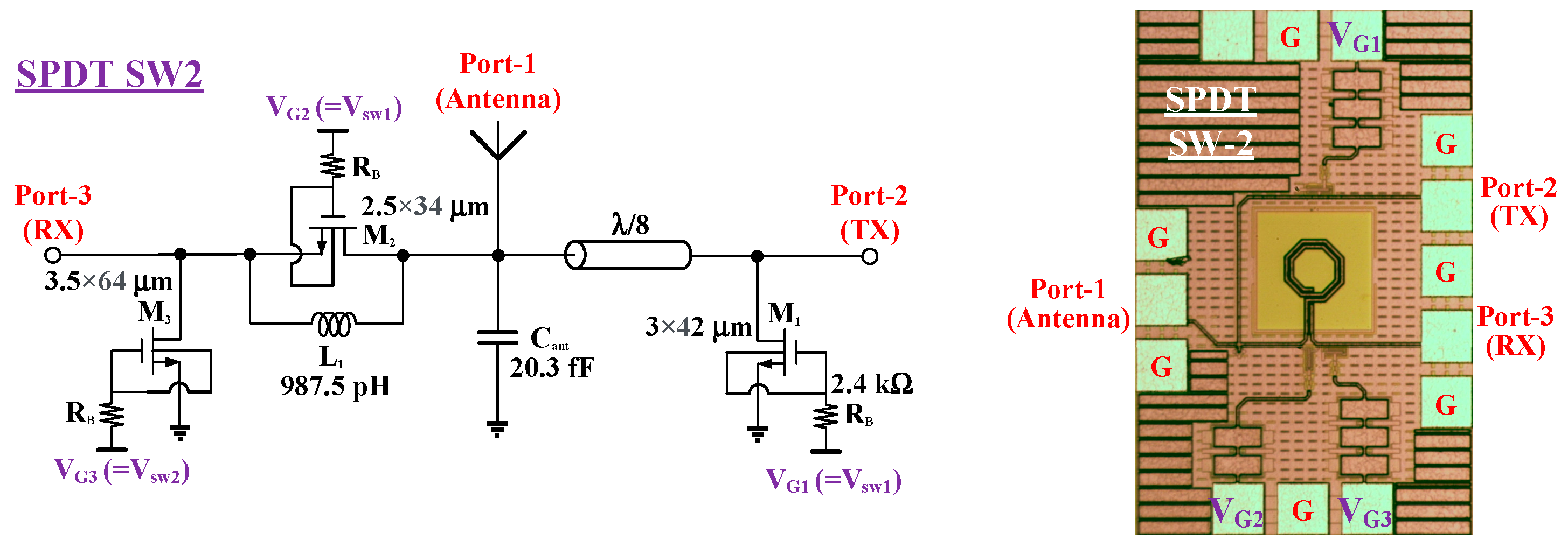
Figure 2 shows a circuit diagram and chip photo of SPDT SW2. The transistor size and important component parameters are also labeled. The chip area, excluding the DC and RF pads, is 0.26 × 0.26 mm
2, i.e., 0.068 mm
2. R
B values of 4.2 kΩ and 2.4 kΩ are used for SPDT SW1 and SPDT SW2, respectively. In the TX path, a parallel DTMOS-R, a series TL (equivalent λ/4 TL), and parallel capacitance, C
ant, are included for a low IL in the TX mode and decent isolation in the RX mode. In the RX path, a series impedance and a parallel DTMOS-R are included for a high-P
1dB in the RX mode and decent isolation in the TX mode.
2. SPDT Switch Design
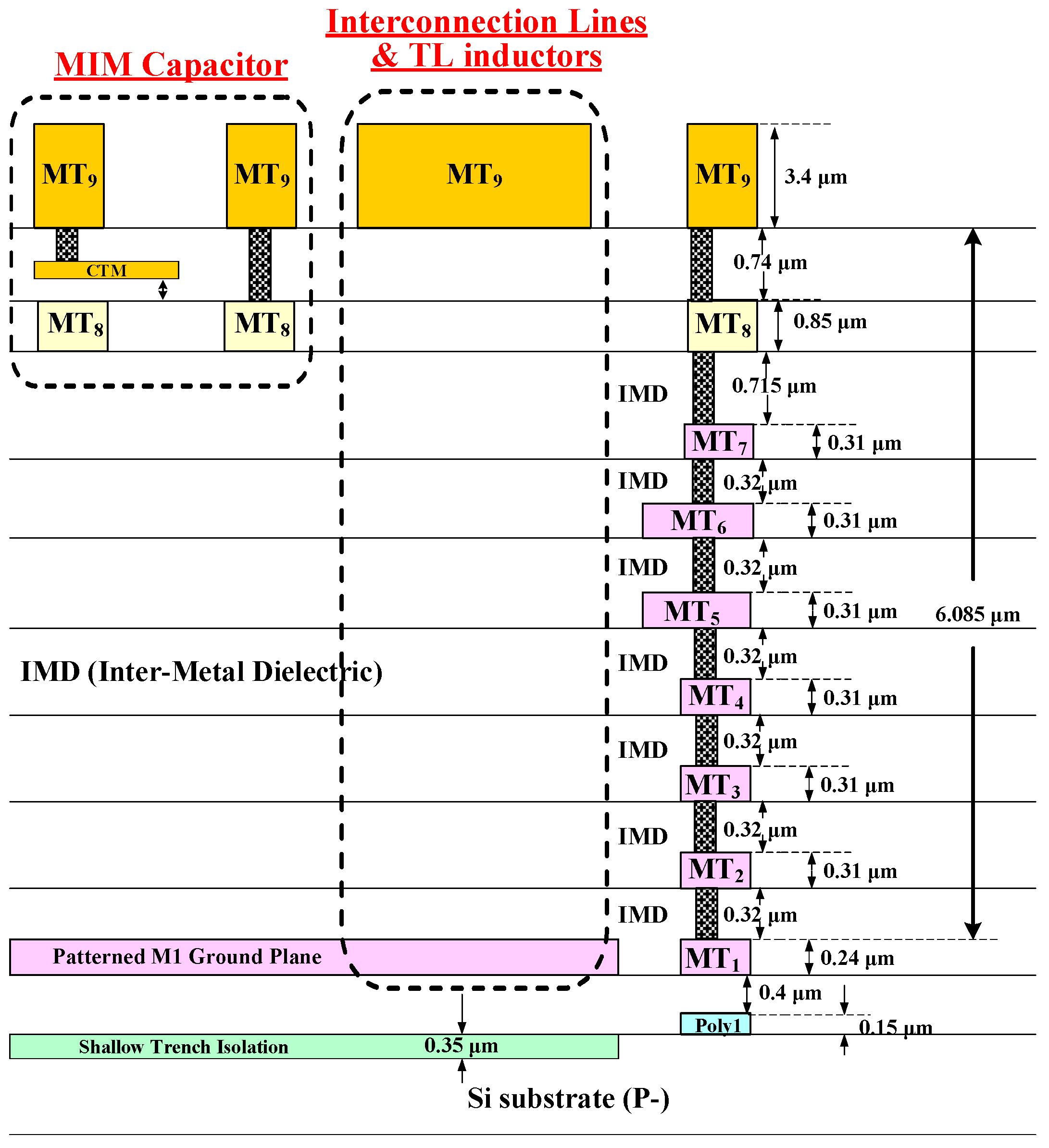
The SPDT SW1 is designed via a 1P9M 90 nm CMOS process.
Figure 3 shows a cross-sectional illustration diagram of the 90 nm CMOS process. The interconnection lines and the TL inductors are placed on the 3.4 μm thick topmost metal (MT
9) to minimize the resistive loss. The bottom-most metal (MT
1) with a pattern density of 70% is used as the ground plane of the TLs. The distance (D) between MT
9 and MT
1 is 6.085 μm. To avoid performance degradation, the space between the TLs is at least 5 times that of D (i.e., 30.425 μm) to control the mutual coupling and parasitics [
17,
18,
19,
20]. The RX path is an L-network constituting a series impedance (of a parallel inductance L
1 and a DTMOS-R M
2) and a parallel DTMOS-R M
3. This leads to high linearity in the RX mode and decent isolation in the TX mode. Moreover, the TX path is a π-network consisting of a parallel DTMOS-R M
1, a series λ/8 TL, and a parallel capacitance, C
ant. A Low IL in the TX mode and good isolation in the RX mode are achieved since the series λ/8-TL in conjunction with the parallel C
ant and parasitic capacitance of the DTMOS-R transistors M
1/M
2 constitute an equivalent λ/4-TL with a characteristic impedance (Z
C) of 50 Ω. The gate width of transistors M
1/M
2 (96-/125 μm for SPDT SW1) is determined according to the required parallel capacitance, C
P (in
Figure 4), to constitute a λ/8-TL-based λ/4-TL in the TX path. A DTMOS-R transistor, M
3, with a relatively large gate width (168 μm for SPDT SW1) is adopted to achieve a better TX-to-RX isolation in the TX mode. The cost is a slight increase in IL in the RX mode due to lower off-state parallel resistance R
off3. In other words, a trade-off exists between the TX-to-RX isolation in the TX mode and the IL in the RX mode.
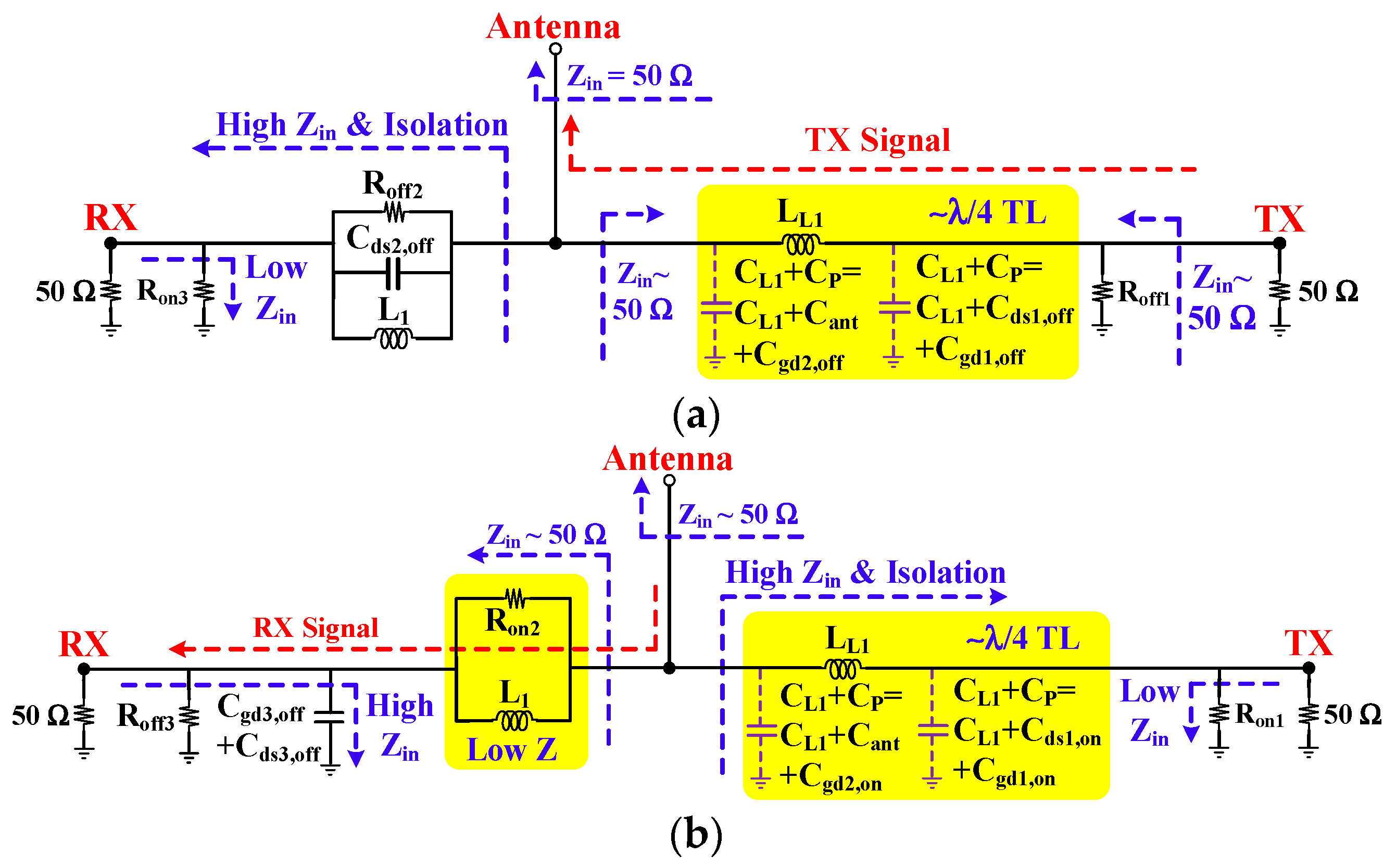
The reason why the L-type network (in both the RX path and TX path) of the SPDT switch can achieve high linearity and decent isolation in both the RX and TX modes can be explained in more detail as follows. Ideally, in the RX mode, transistors M1 and M2 are in the on-state (i.e., short circuit) and M3 is in the off-state (i.e., open circuit). The λ/8-TL, parallel Cant, and parallel capacitance of M1/M2 constitute an equivalent λ/4-TL, leading to an infinite input impedance Zin (i.e., open circuit) looking from the antenna node to the TX node since a short-circuit-loaded λ/4-TL exhibits an infinite Zin. That is, ideally, perfect (antenna-to-TX) isolation in the RX mode is achieved. And perfect IL, linearity, and Zin matching (at the RX and antenna nodes) are also achieved. Moreover, ideally, in the TX mode, transistors M1 and M2 are in the off-state (i.e., open circuit) and M3 is in the on-state (i.e., short circuit). Inductance L1 and the off-state capacitance Cds2,off of M2 are in parallel resonance (i.e., open circuit) at an operation frequency of 28 GHz, leading to an infinite Zin (i.e., open circuit) looking from the antenna node to the RX node. The λ/8-TL, parallel Cant, and parallel capacitance of M1/M2 constitute an equivalent λ/4-TL with a ZC of 50 Ω. That is, ideally, no IL in the TX mode is achieved due to the lossless equivalent λ/4-TL with a ZC of 50 Ω in the TX path and an open circuit of the RX path. And perfect (TX-to-RX) isolation, linearity, and Zin matching (at the TX and antenna nodes) are also achieved.
The reason why a series DTMOS-R transistor is used in the RX path but not adopted in the TX path is for achieving a lower IL, higher linearity, and a better isolation in the TX mode. This can be explained in more detail as follows. To avoid high power loss in the high-output-power TX path, low IL and high linearity are essential for the TX path of an SPDT switch. Compared with a series active DTMOS-R transistor in the on-state, a series passive TL shows a lower IL and higher linearity (due to its metal-based structure). Moreover, compared with an equivalent λ/4-TL with a short-circuited load, a series DTMOS-R transistor in the off-state normally shows a better open circuit (needed for the high isolation operation of the RX path in the TX mode) due to the switching property of the transistor. Therefore, a series DTMOS-R transistor is used in the RX path. Instead of using a series DTMOS-R transistor (in the RX path), a λ/8-TL-based λ/4-TL is used in the TX path for a low IL, high linearity, and high isolation.
The SPDT SW2 is designed via a 1P6M 0.18 μm CMOS process. The interconnection lines and the inductors are placed on the 2.34 μm thick MT6 to minimize the resistive loss. The lowermost MT1 with a pattern density of 90% is used as the ground plane of the TLs. The D between MT6 and MT1 is 5.14 μm. To avoid performance degradation, the space between the TLs is at least 5 times that of D (i.e., 25.7 μm) to control the mutual coupling and parasitics. The design and simulation of the spiral inductor L1 and the λ/8-TL are conducted using ADS Momentum, a 2.5D EM piece of simulation software (suitable for the planar inductor and TL simulation) provided by Agilent Technologies, Santa Clara, United States. Then, EM-circuit co-simulation is performed using ADS to ensure the post-layout simulation results are close to the measured ones.
For the CMOS SPDT switches in the literature, a gate voltage (or control voltage) V
G of 1.8 V is normally adopted to turn on the switch transistors, and a V
G of −1.8 V is normally used to turn off the switch transistors. For a fair comparison, V
G values of 1.8 V and −1.8 V, respectively, are adopted to turn on and turn off the switch transistors in this work. To obtain a better IL, isolation, and linearity performance, a V
G slightly higher than 1.8 V can be adopted to turn on the switch transistors to achieve a better on-state (i.e., lower on-state channel resistance), and a V
G slightly lower than −1.8 V can be adopted to turn off the switch transistors to achieve a better off-state (i.e., higher off-state channel resistance).
Figure 4a shows the equivalent circuit of the SPDT switch in the TX mode. The control voltage V
sw1 (=V
G1 = V
G2) is equal to −1.8 V, and V
sw2 (=V
G3) is equal to 1.8 V. That is, transistors M
1 and M
2 (controlled by V
sw1) are in the off-state and M
3 (controlled by V
sw2) is in the on-state. Ideally, R
off1 and R
off2 are high-resistance and R
on3 is low-resistance (close to 0). According to the TL theory, the series λ/8-TL is equivalent to a series inductance L
L1 and two parallel end-capacitance C
L1. The π-network consisting of a parallel end-capacitance C
L1+ C
ds1,off +C
gd1,off (i.e., C
L1 + C
P), a series inductance L
L1, and a parallel end-capacitance C
L1 + C
ant + C
gd2,off (i.e., C
L1 + C
P) in the TX path is equivalent to a λ/4-TL with a Z
C of 50 Ω. The parallel C
ds2,off and L
1 in the RX path are designed to be in resonance and open at a center frequency of 28 GHz. This leads to decent input impedance matching at the TX and antenna nodes (i.e., a decent S
11 and S
33), a low IL, and high TX-to-RX isolation. This can be explained in more detail as follows. In the RX path of the SPDT switch, inductor L
1 is in parallel with DTMOS-R M
2. In the RX mode, DTMOS-R M
2 is in the on-state, equivalent to a small resistance R
on2,to achieve a decent IL. L
1 is negligible since R
on2 dominates the RX path impedance. In the TX mode, DTMOS-R M
2 is in the off-state, equivalent to a large resistance R
off2, in parallel with a capacitance C
ds2,off. To achieve decent isolation with the RX path, L
1 and C
ds2,off should be in parallel resonance at an operation frequency of 28 GHz. For SPDT SW1, C
ds2,off is equal to 74.9 fF, so an L
1 of 431.3 pH is chosen. For SPDT SW2, C
ds2,off is equal to 32.7 fF, so an L
1 of 987.5 pH is used.
The design and simulation of the λ/8-TL-based equivalent λ/4-TL in the TX path can be explained in more detail as follows. According to the TL theory, the ABCD matrix of a lossless TL with electrical length of θ is given by [
21]
From (1), Z
C and θ can be written as
That is, the Z
C and θ of a TL can be obtained from the simulated ABCD-parameters converted from the simulated S-parameters. For a lossless TL with a θ of 90° (i.e., length of λ/4) and Z
C of R
0 (i.e., 50 Ω), (1) can be simplified as
Additionally, the lossless TL can be modeled by a π-network consisting of a series inductor (L
L) and two parallel end capacitors (C
L). The ABCD matrix of the π-network is given by
If we let (5) equal (4), we obtain
In
Figure 4a, two additional parallel capacitances C
P (equal to C
ds1,off + C
gd1,off or C
ant+ C
gd2,off) are incorporated to the shorter (electrical length θ
1 of 45° or length of λ/8 in this work) TL with a Z
C of Z
C1 to form an equivalent λ/4 TL. It has the potential of a small chip area since the TL θ
1 (45° in this work) can be any value less than or equal to 90° in theory. For the TL, suppose the corresponding L
L is L
L1, and C
L is C
L1. From (1) and (5), L
L1 and C
L1 can be written as
The equivalence of the λ/8 TL with a Z
C of Z
C1 (i.e., C
L1-L
L1-C
L1 π-network) and two additional parallel capacitances (C
P) to a λ/4 TL with a Z
C of R
0 (i.e., C
L-L
L-C
L π-network) requires L
L1 = L
L and C
L1 + C
P = C
L. This leads to Z
C1 and C
P, given by
In this work, θ1 is equal to 45° (i.e., length of λ/8). From (10) and (11), the required ZC1 of the λ/8-TL is 70.7 Ω, and the required additional parallel capacitance, CP, is 80.4 fF.
Figure 4b shows the equivalent circuit of the SPDT switch in the RX mode. The control voltage V
sw1 is equal to 1.8 V and V
sw2 is equal to −1.8 V. That is, transistors M
1 and M
2 are in the on-state and M
3 is in the off-state. Ideally, R
on1 and R
on2 are low-resistance (close to 0) and R
off3 is high-resistance. The π-network consisting of parallel end-capacitance (C
L1 + C
ds1,on + C
gd1,on), series inductance (L
L1), and parallel end-capacitance (C
L1 + C
ant + C
gd2,on) in the TX path is roughly equivalent to a λ/4-TL with characteristic impedance of 50 Ω. Z
in looking from the antenna node to the TX node is infinite (i.e., an open circuit) since a short-circuit-loaded λ/4-TL exhibits an infinite Z
in. The parallel R
on2 and L
1 in the RX path is low-impedance (close to 0). This leads to decent input impedance matching at the RX and antenna nodes (i.e., a decent S
11 and S
22), a low IL, and high antenna-to-TX isolation.
In the TX path of the SPDT switch, the series λ/8-TL has a Z
C of 70.7 Ω. The λ/8-TL in conjunction with the end-capacitance contribution from the DTMOS-R transistors, M
1 and M
2, and capacitance, C
ant, constitutes a λ/4-TL with a Z
C of 50 Ω (according to Equations (10) and (11)).
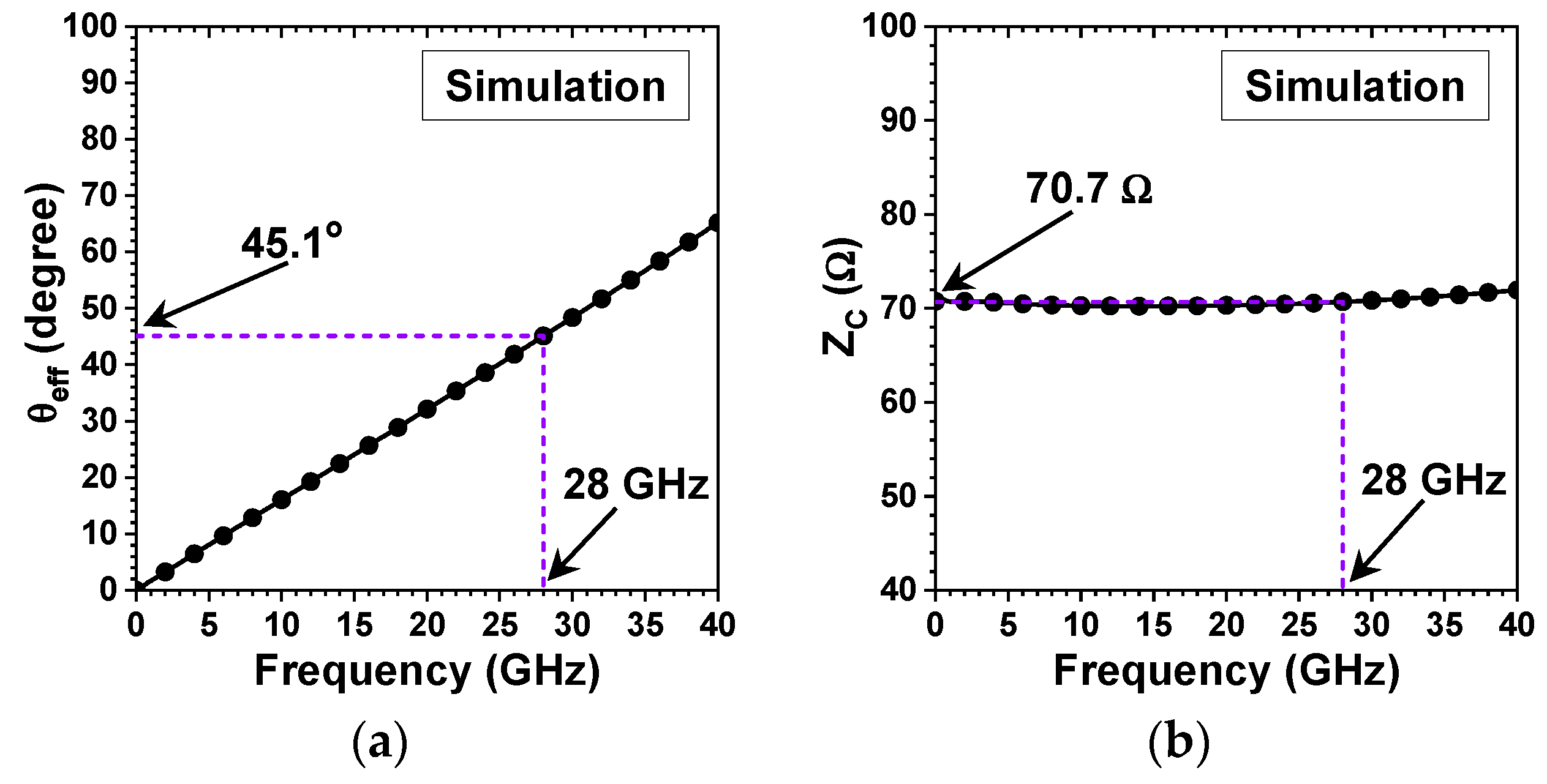
Figure 5a shows the simulated equivalent electrical length (θ
eff) versus the frequency characteristics of the TL in the TX path of SPDT SW1 according to Equation (3). The simulated ABCD parameters are converted from the simulated S-parameters. At 28 GHz, the corresponding θ
eff is 45.1
o (about λ/4), consistent with the theoretical analysis.
Figure 5b shows the simulated Z
C versus the frequency characteristics of the TL in the TX path of SPDT SW1 according to Equation (2). At 28 GHz, the corresponding Z
C is 70.7 Ω; the same applies to the theoretical value.
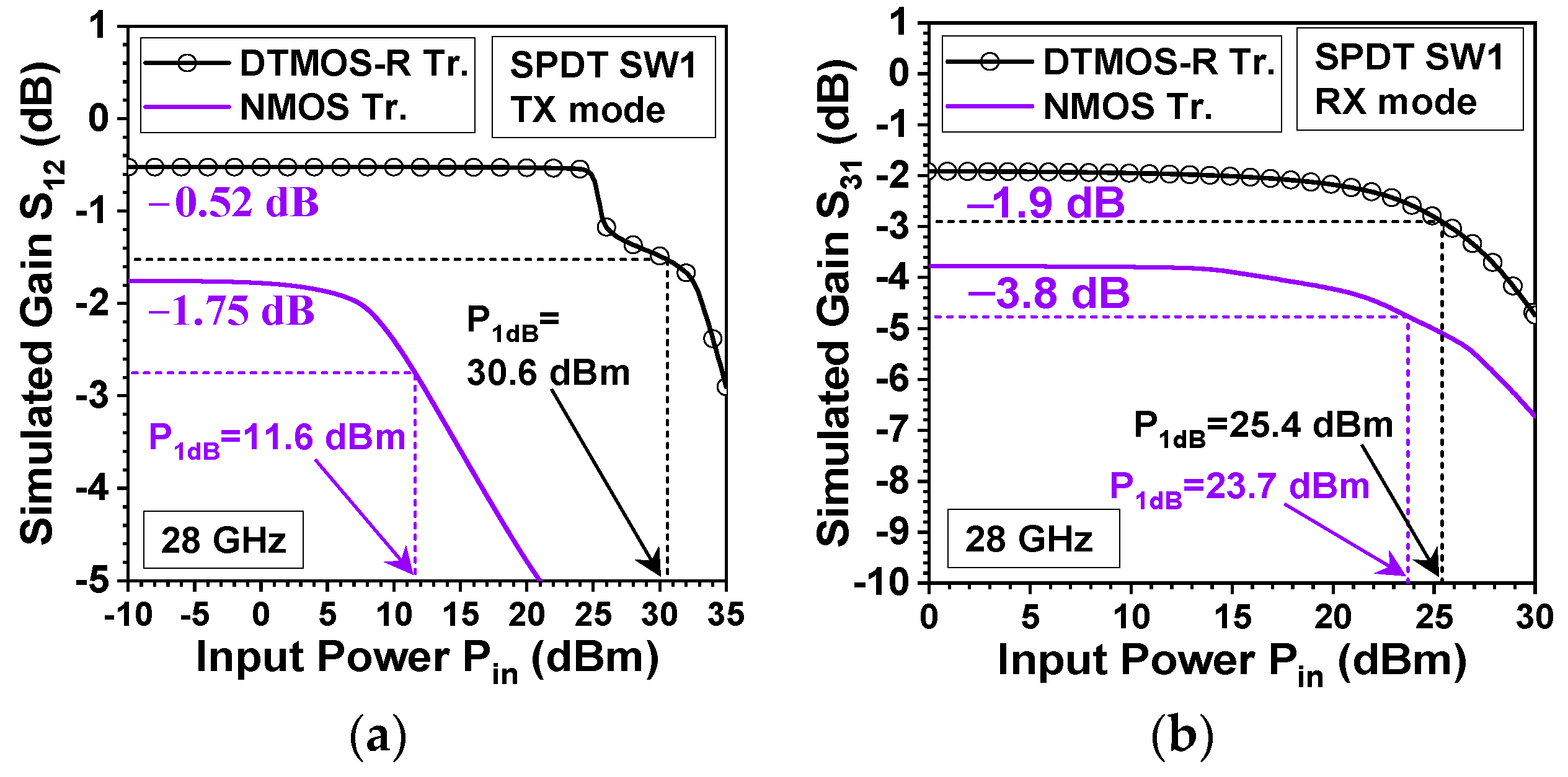
Figure 6a shows the simulated P
1dB of SPDT SW1 in the TX mode using the proposed DTMOS-R switching transistors and the traditional NMOS switching transistors. In the case of using DTMOS-R switching transistors, SPDT SW1 achieves a simulated IL of 0.52 dB (at a low P
in of −10 dBm) and P
1dB of 30.6 dBm. These results are better than those (simulated IL of 1.75 dB (at a low P
in of −10 dBm) and P
1dB of 11.6 dBm) using traditional NMOS switching transistors.
Figure 6b shows the simulated P
1dB of SPDT SW1 in the RX mode using the proposed DTMOS-R switching transistors and the traditional NMOS switching transistors. In the case of using DTMOS-R switching transistors, SPDT SW1 achieves a simulated IL of 1.9 dB (at a low P
in of −10 dBm) and P
1dB of 25.4 dBm. These results are better than those (simulated IL of 3.8 dB (at a low P
in of −10 dBm) and P
1dB of 23.7 dBm) using traditional NMOS switching transistors. Overall, these results show that the proposed body-floating technique, i.e., the DTMOS-R switching transistors technique, in this work is effective for the IL and P
1dB enhancement of SPDT SW1 in both the TX and RX modes.
3. Results and Discussion of SPDT SW1
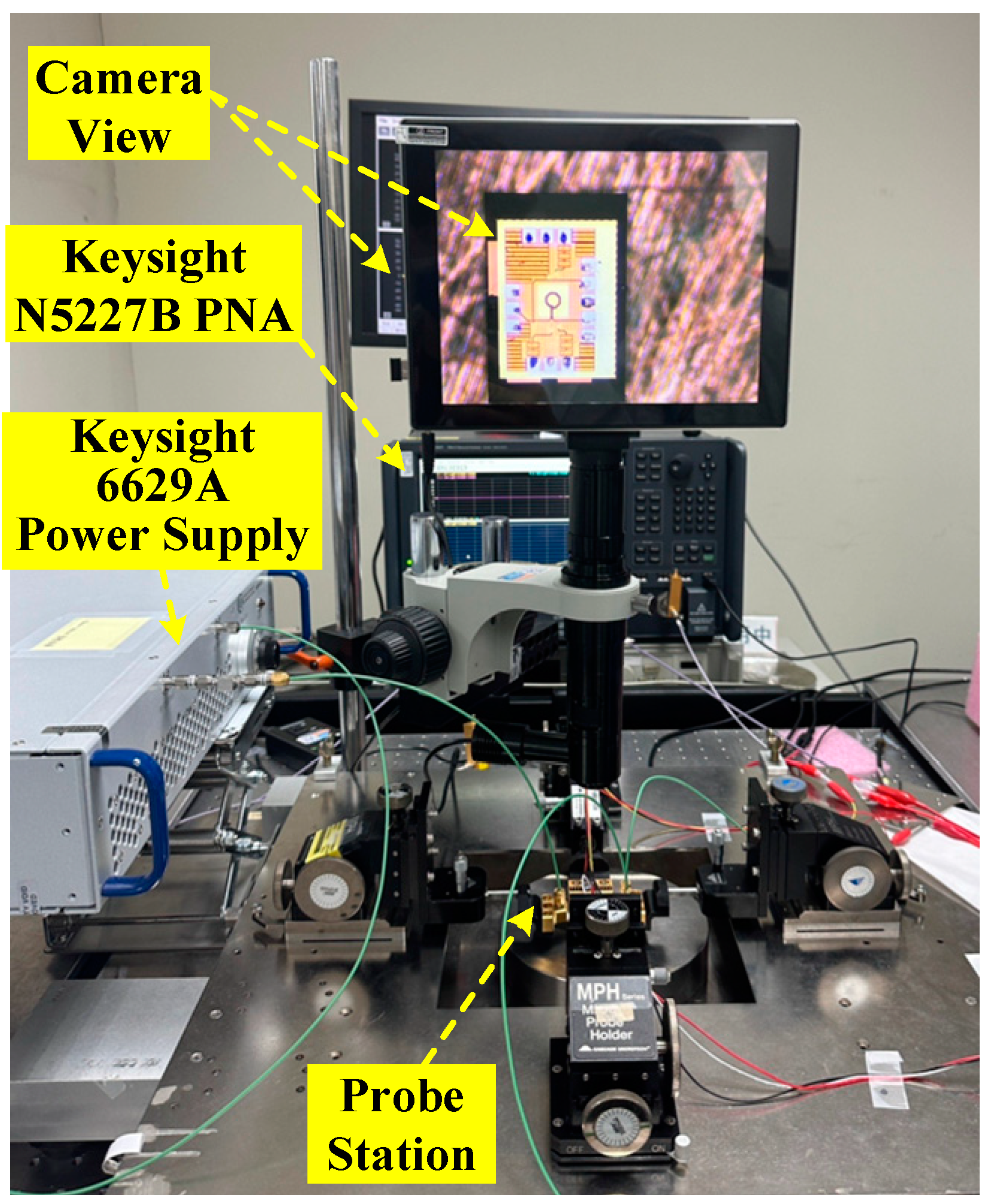
The on-wafer S-parameter measurements of SPDT SW1 and SW2 were performed using a Keysight N5227B PNA microwave network analyzer, as shown in
Figure 7.
Figure 8a shows the measured and simulated IL (i.e., lS
12l) and isolation (i.e., lS
32l) of SPDT SW1 in the TX mode. SPDT SW1 achieves a measured minimum IL (IL
min) of 0.58 dB at 24.8 GHz and an IL better than 1 dB for 17–34.9 GHz, corresponding to a 1 dB bandwidth (f
1dB) of 17.9 GHz. This result is close to the simulated one, i.e., an IL
min of 0.47 dB at 25 GHz and an IL lower than 1 dB for 15.1–39.4 GHz, corresponding to an f
1dB of 24.3 GHz. This decent IL is attributed to the low loss of the equivalent λ/4-TL, the good TX-RX isolation, and the high impedance of the off-state DTMOS-R M
1. Moreover, SPDT SW1 achieves a measured maximum isolation (lS
32l
max) of 62.3 dB at 31.4 GHz and isolation of 25.6–62.3 dB for 17–34.9 GHz. This result is close to the simulated one, i.e., an lS
32l
max of 59.5 dB at 31.7 GHz and isolation of 27.7–59.5 dB for 17–34.9 GHz.
Figure 8b shows the measured and simulated S
11 and S
22 of SPDT SW1 in the TX mode. SPDT SW1 achieves a measured minimum S
11 (S
11,min) of −21.9 dB at 23.7 GHz and S
11 better than −15 dB for 18.4–31.4 GHz, equivalent to a −15 dB input matching bandwidth (f
15dB) of 13 GHz. This result is close to the simulated one, i.e., an S
11,min of −37.6 dB at 25.9 GHz and an f
15dB of 16.4 GHz (18.8–35.2 GHz). Moreover, SPDT SW1 achieves a measured minimum S
22 (S
22,min) of −30.6 dB at 26.8 GHz and an S
22 better than −15 dB for 18.9–39.2 GHz, equivalent to an f
15dB of 20.3 GHz. This result is close to the simulated one, i.e., an S
22,min of −43.5 dB at 26.8 GHz and an f
15dB of 18.9 GHz (18.8–37.7 GHz).
Figure 8c shows the measured and simulated IL (i.e., lS
31l) and isolation (i.e., lS
21l) of SPDT SW1 in the RX mode. SPDT SW1 achieves a measured IL
min of 1.83 dB at 30.9 GHz and an IL of 1.83–2.1 dB for 25–38.3 GHz. This result is close to the simulated one, i.e., an IL
min of 1.33 dB at 38.4 GHz and an IL of 1.33–2.1 dB from 26.6 GHz to over 50 GHz. Moreover, SPDT SW1 achieves a measured isolation of 24.5–27 dB for 25–38.3 GHz. This result is close to the simulated one, i.e., an isolation of 22.2–25.1 dB for 25–38.3 GHz.
Figure 8d shows the measured and simulated S
11 and S
33 of SPDT SW1 in the RX mode. SPDT SW1 achieves a measured S
11,min of −14.7 dB at 30.9 GHz and an S
11 better than −10 dB for 20.7–50 GHz, corresponding to an f
10dB of 29.3 GHz. This result is consistent with the simulated one, i.e., an S
11,min of −12.7 dB at 36.8 GHz and an f
10dB of 17.7 GHz (29.1–46.8 GHz). Moreover, SPDT SW1 achieves a measured minimum S
33 (S
33,min) of −30.4 dB at 29 GHz and an S
33 better than −10 dB for 18.1–44.9 GHz, equivalent to f
10dB of 26.8 GHz. This result is consistent with the simulated one, i.e., an S
33,min of −31.1 dB at 32.4 GHz and an f
10dB of 25.6 GHz (20.9–46.5 GHz).
Figure 9a shows the measured and simulated power gain S
12 (i.e., P
out−P
in in dBm) against the input power (P
in) characteristics of SPDT SW1 at 28 GHz in the TX mode. That is, DTMOS-R M
1 and M
2 (controlled by V
sw1) are in the off-state and M
3 (controlled by V
sw2) is in the on-state. SPDT SW1 achieves a measured S
12 of −0.67 dB at a low P
in of 0 dBm and an S
12 of −1.67 dB at a high P
in of 28.5 dBm. The corresponding P
1dB is 28.5 dBm. This result is consistent with the simulated one, i.e., an S
12 of −0.52 dB at a low P
in of 0 dBm and an S
12 of −1.52 dB at a high P
in of 30.6 dBm, corresponding to simulated P
1dB of 30.6 dBm. The decent P
1dB performance of SPDT SW1 in the TX mode is mainly attributed to the novel SPDT switch topology and the adoption of DTMOS-R switch transistors. This can be explained in more detail as follows. In contrast to the traditional common-source (CS) switch transistors using a V
sw1/ V
sw2 of 0/V
DD and a body voltage of 0 V, DTMOS-R M
1 and M
2 achieve a better off-states due to higher off-state channel/substrate resistance (R
off,ch/R
off,sub) because of a higher threshold voltage (V
th) and the suppression of substrate leakage (I
B). Moreover, DTMOS-R M
3 achieves a better on-state due to lower on-state channel/substrate resistance (R
on,ch/R
on,sub) because of a lower V
th, i.e., a higher over-drive voltage V
ov (=V
gs−V
th). In other words, a higher P
in (with a more negative peak voltage) is required to conduct the off-state shunt/series M
1/M
2. This leads to a high P
1dB in the TX mode. Moreover, the high P
1dB of 28.5 dBm is partly due to the prominent TX-to-RX isolation of 62.3 dB (see
Figure 8a).
Figure 9b shows the measured and simulated power gain S
31 against P
in the characteristics of SPDT SW1 at 28 GHz in the RX mode. That is, DTMOS-R M
1 and M
2 are in the on-state and M
3 is in the off-state. SPDT SW1 achieves a measured S
31 of −1.9 dB at a low P
in of 0 dBm and −2.9 dB at a high P
in of 24 dBm. The corresponding P
1dB is 24 dBm. This result is consistent with the simulated one, i.e., an S
12 of −1.91 dB at a low P
in of 0 dBm and an S
12 of −2.91 dB at a high P
in of 25.4 dBm, corresponding to a simulated P
1dB of 25.4 dBm. This decent P
1dB performance of the SPDT switch in the RX mode is also attributed to the novel SPDT switch topology and the adoption of DTMOS-R switch transistors.
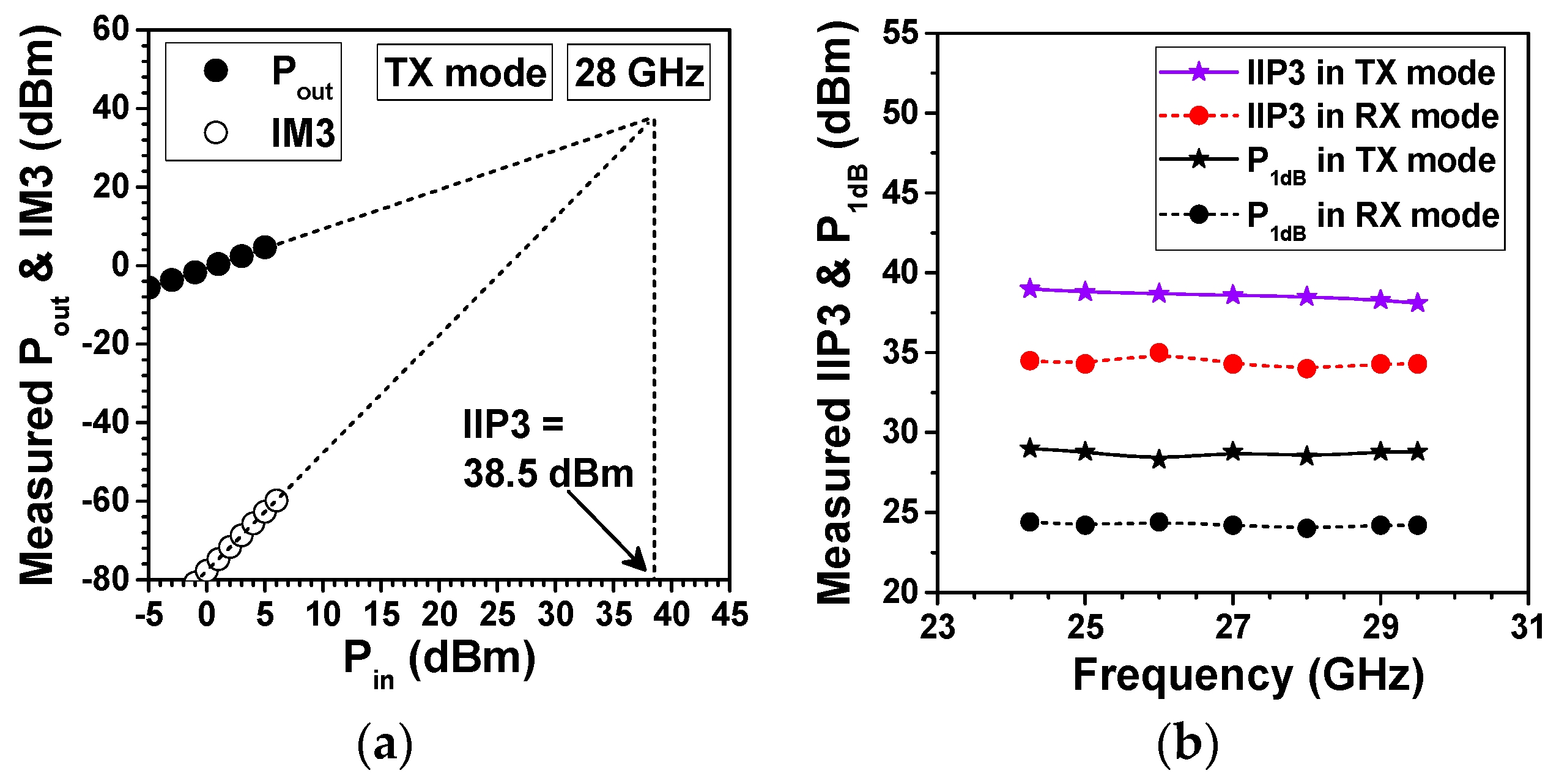
Figure 10a shows the measured fundamental (P
out) and third-order intermodulation output power (IM3) versus the P
in characteristics of SPDT SW1 in the TX mode at 28 GHz. SPDT SW1 achieves an excellent IIP3 of 38.5 dBm.
Figure 10b shows the measured P
1dB and IIP3 versus the frequency characteristics of SPDT SW1 over the 24.25–29.5 GHz (N257/N258) 5G mm wave band. SPDT SW1 achieves a P
1dB of 28–29 dBm and an IIP3 of 38.1–39 dBm in the TX mode, and a P
1dB of 24–24.8 dBm and an IIP3 of 34.1–35 dBm in the RX mode. This result is reasonable since it is consistent with the theoretical analysis, i.e., IIP3 is about 9.6 dBm larger than P
1dB [
17].
4. Results and Discussion of SPDT SW2
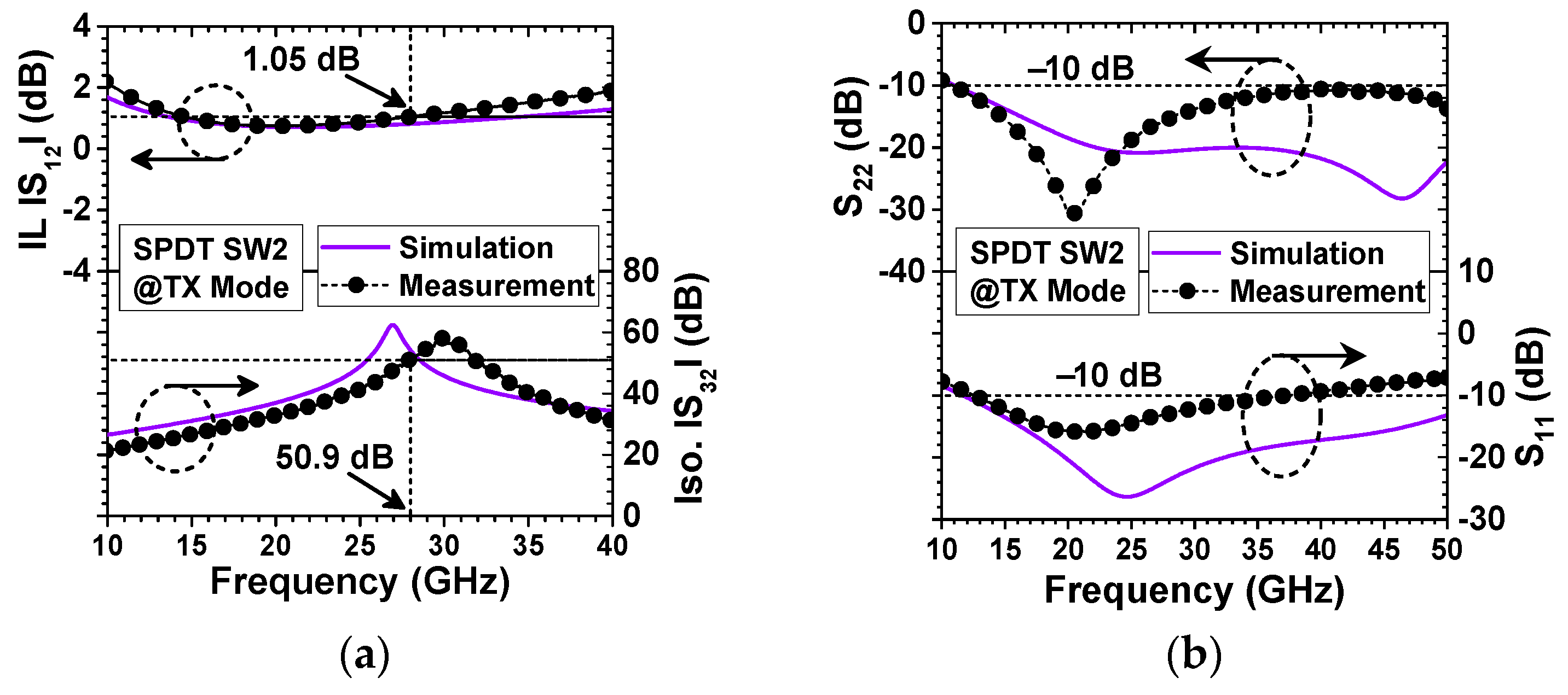
Figure 11a shows the measured and simulated IL (i.e., lS
12l) and isolation (i.e., lS
32l) of SPDT SW2 in the TX mode. SPDT SW2 achieves a measured IL
min of 0.74 dB at 20.2 GHz and an IL better than 1.2 dB for 13.6–30.5 GHz, corresponding to a bandwidth of 16.9 GHz. This result is close to the simulated one, i.e., an IL
min of 0.7 dB at 21.5 GHz and an IL lower than 1.2 dB for 12.4–38.1 GHz, corresponding to a bandwidth of 25.7 GHz. The decent IL is attributed to the low-loss of the equivalent λ/4-TL, the good TX-to-RX isolation, and the high impedance of the off-state DTMOS-R M
1. Moreover, SPDT SW2 achieves a measured lS
32l
max of 59.2 dB at 30 GHz and isolation of 25.2–59.2 dB for 13.6–30.5 GHz. This result is close to the simulated one, i.e., an lS
32l
max of 62.4 dB at 26.9 GHz and isolation of 29.7–62.4 dB for 13.6–30.5 GHz.
Figure 11b shows the measured and simulated S
11 and S
22 of SPDT SW2 in the TX mode. SPDT SW2 achieves a measured S
11,min of −15.9 dB at 20.2 GHz and an S
11 better than −10 dB for 12.6–37.3 GHz, equivalent to an f
10dB of 24.7 GHz. This result is close to the simulated one, i.e., an S
11,min of −26.4 dB at 24.7 GHz and an f
10dB larger than 38.4 GHz (11.6–50 GHz). Moreover, SPDT SW2 achieves a measured S
22,min of −30.7 dB at 20.7 GHz and an S
22 better than −10 dB from 10.9 GHz to larger than 50 GHz, equivalent to an f
10dB larger than 39.1 GHz. This result is close to the simulated one, i.e., an S
22,min of −28.2 dB at 46.4 GHz and an f
10dB larger than 39 GHz (11–50 GHz).
Figure 11c shows the measured and simulated IL (i.e., lS
31l) and isolation (i.e., lS
21l) of SPDT SW2 in the RX mode. SPDT SW2 achieves a measured IL
min of 1.93 dB at 40.2 GHz and an IL of 1.93–2.5 dB from 27.7 GHz to over 50 GHz. This result is close to the simulated one, i.e., an IL
min of 1.99 dB at 34.2 GHz and an IL of 1.99–2.5 dB for 25.9–43.9 GHz. Moreover, SPDT SW2 achieves a measured isolation of 17.5–21.8 dB for 27.7–50 GHz. This result is close to the simulated one, i.e., isolation of 19.5–26.2 dB for 27.7–50 GHz.
Figure 11d shows the measured and simulated S
11 and S
33 of SPDT SW2 in the RX mode. SPDT SW2 achieves a measured S
11,min of −13 dB at 41.4 GHz and an S
11 better than −10 dB from 27 GHz to over 50 GHz, corresponding to an f
10dB larger than 23 GHz. This result is consistent with the simulated one, i.e., an S
11,min of −12.9 dB at 35.3 GHz and an f
10dB of 16.9 GHz (27.6–44.5 GHz). Moreover, SPDT SW2 achieves a measured S
33,min of −49.2 dB at 31.4 GHz, and an S
33 better than −10 dB for 11–48.5 GHz, equivalent to an f
10dB of 37.5 GHz. This result is consistent with the simulated one, i.e., an S
33,min of −44.1 dB at 28.5 GHz and an f
10dB of 23.3 GHz (17.1–40.4 GHz).
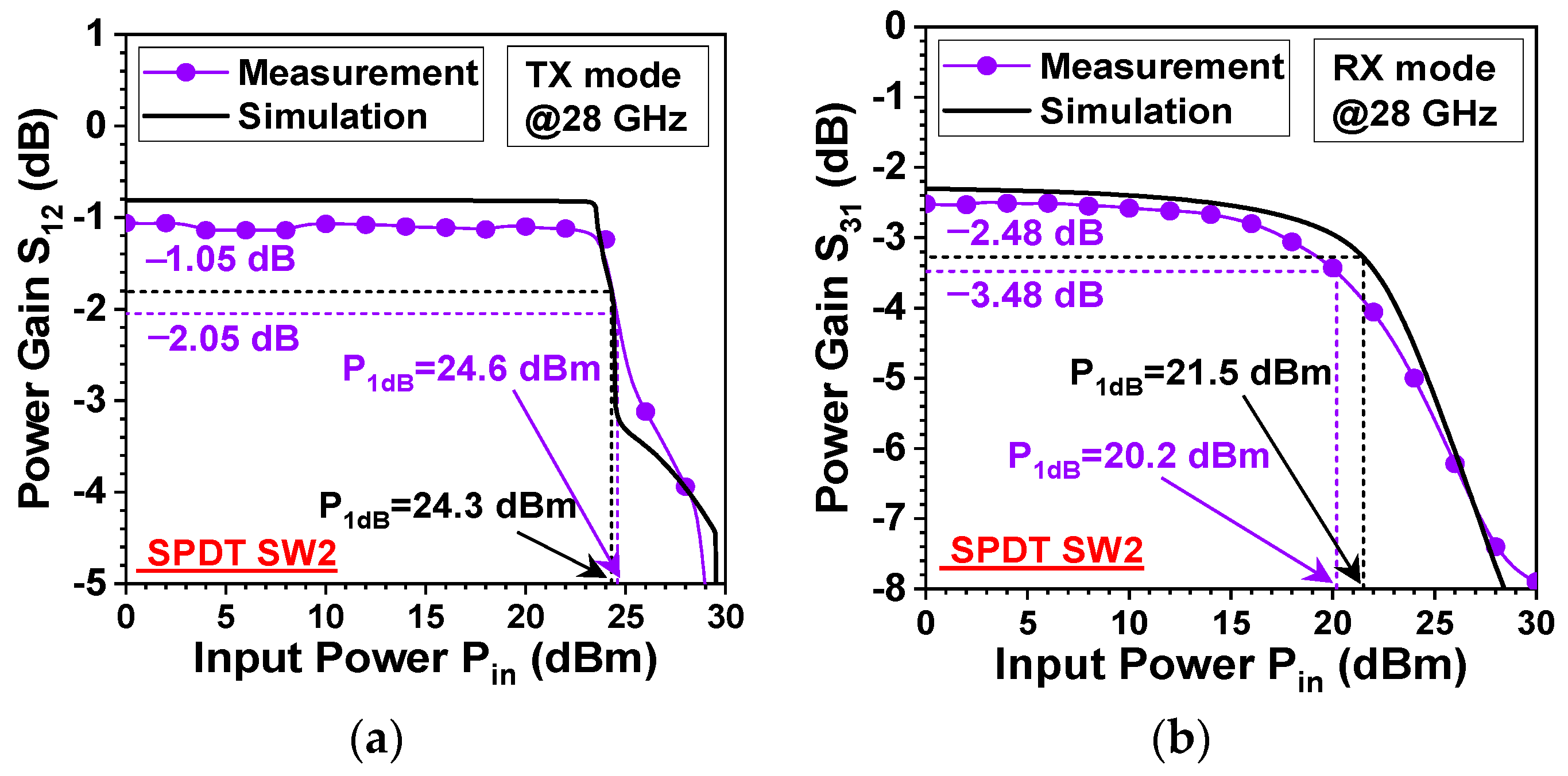
Figure 12a shows the measured and simulated power gain S
12 against the P
in characteristics of SPDT SW2 at 28 GHz in the TX mode. That is, DTMOS-R M
1 and M
2 are in the off-state and M
3 is in the on-state. SPDT SW2 achieves a measured S
12 of −1.05 dB at a low P
in of 0 dBm and an S
12 of −2.05 dB at a high P
in of 24.6 dBm. The corresponding P
1dB is 24.6 dBm. This result is consistent with the simulated one, i.e., an S
12 of −0.81 dB at a low P
in of 0 dBm and an S
12 of −1.81 dB at a high P
in of 24.3 dBm, corresponding to a simulated P
1dB of 24.3 dBm. The decent P
1dB performance of SPDT SW2 in the TX mode is mainly attributed to the novel SPDT switch topology and the adoption of DTMOS-R switch transistors. This can be explained in more detail as follows. In contrast to the traditional CS switch transistors using a V
sw1/V
sw2 of 0/V
DD and a body voltage of 0 V, DTMOS-R M
1 and M
2 achieve a better off-state due to higher off-state channel/substrate resistance (R
off,ch/R
off,sub) because of a higher V
th, a lower overdrive voltage V
ov, and the suppression of I
B. Moreover, DTMOS-R M
3 achieves a better on-state due to lower on-state channel/substrate resistance (R
on,ch/R
on,sub) because of a lower V
th and a higher over-drive voltage V
ov. In other words, a higher P
in is required to conduct the off-state shunt/series M
1/M
2. This leads to a high P
1dB in the TX mode. Moreover, the high P
1dB of 24.6 dBm is partly due to the prominent (TX-to-RX) isolation of 59.2 dB (see
Figure 11a).
Figure 12b shows the measured power gain S
31 against the P
in characteristics of SPDT SW2 at 28 GHz in the RX mode. That is, DTMOS-R M
1 and M
2 (controlled by V
sw1) are in the on-state, and M
3 (controlled by V
sw2) is in the off-state. The measured result is consistent with the simulated one. SPDT SW2 achieves a measured S
31 of −2.48 dB at a low P
in of 0 dBm, and −3.48 dB at a high P
in of 20.2 dBm. The corresponding P
1dB is 20.2 dBm. This decent P
1dB performance of the SPDT switch in the RX mode is also attributed to the novel SPDT switch topology and the adoption of DTMOS-R switch transistors.
A figure-of-merit (FOM) suitable for the evaluation of a wideband, low-IL, high-linearity, and decent-isolation SPDT switch can be defined as follows.
in which IL [
1] is the insertion loss in magnitude, BW[GHz] is the bandwidth in GHz, Isolation [
1] is the isolation in magnitude, and P
1dB is the input 1 dB compression point in mW.
Table 1 is a summary of SPDT SW1 and SW2, and recently reported state-of-the-art SPDT switches with similar operation frequency using similar CMOS technologies. The operation bandwidth (BW) is a function of the specification of the maximum allowed IL (IL
max). As shown, SPDT SW1 achieves BW values of 13.3 and 21.1 GHz for IL
max of 2.1 and 2.5 dB, respectively. SPDT SW2 achieves a BW of 22.3 GHz for IL
max 2.5 dB. For the same IL
max of 2.5 dB, for a fair comparison, SPDT SW1 achieves a BW of 21.1 GHz, close to that (22.3 GHz) of SPDT SW2. Overall, SPDT SW1 occupies a medium area, and achieves decent reflection coefficients, IL, isolation, bandwidth, and P
1dB, and excellent FOM in the RX mode and the best FOM in the TX mode.


 ,
, 


